Guiding Light in Electro-Optic Polymers

Abstract
: Electro-optic polymers have unique photonic, electro-optic and mechanical properties that make them attractive to use in a wide range of devices starting from ultra-high bandwidth light modulators for optical communications to miniature low power components for on-chip optical interconnects. The main building blocks of those devices are optical waveguides, that due to versatility of the polymers can be fabricated as either traditional multi-layer polymer structures, silicon nano-slots filled with the polymer, or dynamically created waveguides based on field-induced guiding. In this paper we cover various types of waveguides and analyze their optimum designs depending on application.1. Introduction
Electro-optic (EO) polymers are unique materials having many advantages over inorganic materials for the wide range of applications—from optical network components and optical interconnects to millimeter and microwave photonics. They have very large EO coefficients, low optical loss (in the 1.3 and 1.55 μm telecommunication windows), low dispersion of refractive index between optical frequencies and millimeter waves, as well as high bandwidth [1,2]. They are easy to process and have relatively low cost.
Moreover, recently EO polymer modulators were environmental stress tested at both the chip and packaged device level [3]. The study guided by the industry standard Telcordia GR-468 environmental stress specifications with particular attention paid to test regarding thermal and/or photochemical stability demonstrated excellent device performance. Specifically, the devices were thermally stable for over 5,000 h at 85 °C. Furthermore, high optical power (500 mW @ 1,550 nm) tests showed the photochemical stability of the EO polymer material in hermetically sealed packages.
There is a broad range of EO devices that can be fabricated based on these polymers [4] having a waveguide structure as the main building block. In this paper, we review different design configurations and analyze their advantages and limitations. For example, to create a miniature EO light modulator for the highest on-chip integration, size and power efficiency would be critical. This requires integration with silicon photonics and use of either slotted [5] or photonic crystal waveguide [6,7] covered with EO polymer. For an optical network (Internet) the size of the light modulator is less significant, however operating voltage and bandwidth are more important. Therefore, all-polymer and hybrid polymer/sol-gel configurations might be the better choice. Below we consider different parameter that have to be optimized and the corresponding waveguide configuration that can be used.
2. Traditional Polymer Waveguides
Many applications need optical waveguides that confine light in two directions and allow propagation in the third. Such waveguides consist of several thin polymer films. In vertical direction light confinement is done by choosing appropriate refractive indices of the core and the claddings. To create refractive index contrast in horizontal direction at least one of the polymer films has to be patterned. There are several possible fabrication techniques that can be used—photoresist-based patterning, direct photo-lithographic or e-beam patterning, micromolding in capillaries and microcontact printing [4].
2.1. Photoresist-Based Patterned Waveguides
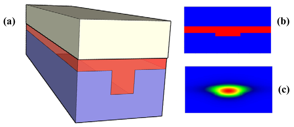
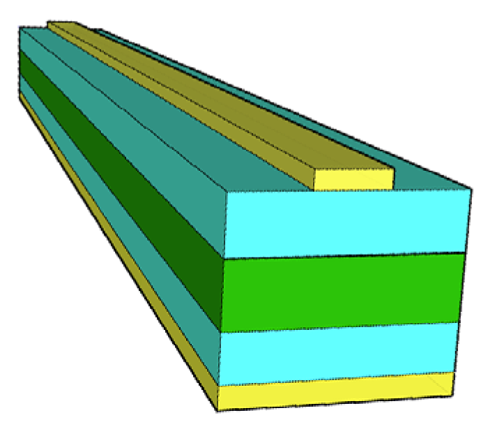
The example of the photoresist-based patterned EO polymer waveguide is shown in Figure 1(a) with 3.2 μm polyurethane lower cladding shown in blue. This layer was patterned using photolithography and then 1.4-mm-high CLD-1/poly-(methylmethacrylate) (PMMA)guiding layer (shown in red), and a 2.9-mm-high ultraviolet light–curable upper cladding layer (white) were spin-coated on top. Figure 1(b,c) illustrate the side view of the device and the typical mode propagating in such waveguide.
This device published in [8] was the first to demonstrate the halfwave voltage Vπ (the voltage needed to switch the device from on- to off-configuration) less than 1 volt at 1.31 micron wavelength. This is one of the critical requirements for ultra-high speed light modulators for fiber optic communication link, because the link gain is inversely proportional to Vπ2 and the noise figure is directly proportional to Vπ2 in the low-gain limit. The link usually includes the optical source, modulator, fiber and optical receiver and has RF input and output ports. The gain is defined as a measure of efficiency in that it is the ratio of the output RF signal power to the input RF signal power. Noise figure expresses the extent to which the signal-to-noise ratio degrades between the input and the output of the link.
2.2. Direct e-Beam Written Waveguides
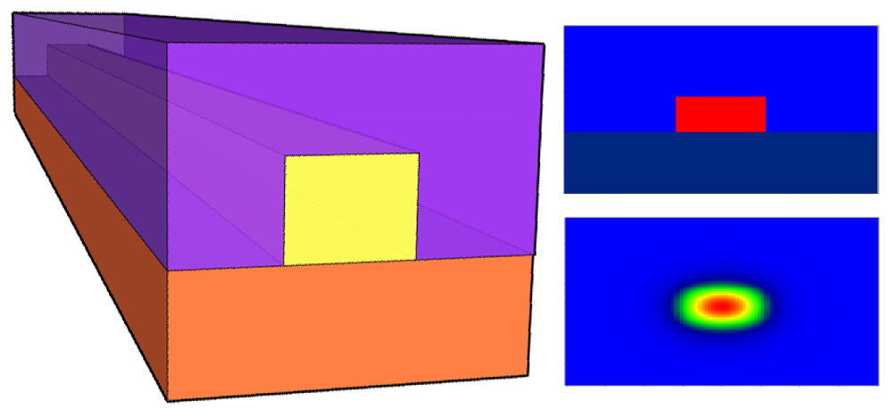
Photolithography gives great results for the simple straight waveguides, but microring resonators and other high Q structures require creation of the waveguides with ultra-smooth walls for very low scattering losses. Direct e-beam patterning of EO polymer waveguides was demonstrated in polymethyl methacrylate (PMMA) polymer matrix doped with organic nonlinear chromophores [9]. The polymer in the exposed regions was removed with the standard electron beam resist developer. This technique allowed creation of high quality smooth waveguide walls and prevented the chromophores from being damaged by the e-beam. It was applied to fabrication of microring resonators with extinction ratios more than 16 dB and quality factors were in the range of 103 ∼ 104. The device structure, side view and the typical mode profile are illustrated in Figure 2.
3. Hybrid Sol-Gel/Polymer Waveguides
There is another important design constraint that always should be taken into consideration while fabricating EO polymer devices. The material has to be poled to be able to change refractive index under applied voltage. This means that the chromophore molecules have to be aligned in the same direction. It requires heating the EO polymer and applying high voltage for initial alignment. Then the polymer is cooled down and the voltage is turned off, so that the orientation of the molecules is fixed and the material is ready for operation. There are two steps that require presence of the electrodes in close proximity to electro-optic polymers—during the poling and during the device operation. These electrodes are not necessary the same. For example, a layer of the electro-optic polymer can be corona-poled or contact-poled, and only several fabrication steps later the second electrode can be added to the device [10].
Traditionally, when the EO properties of the thin polymer film are measured, the film is sandwiched between two electrodes and poled, and then the top electrode is removed and the EO activity is optically tested. Fabrication of high quality devices requires separation of the electrodes from the EO polymer layers by two optical claddings. This might affect poling, since the voltage applied between the electrodes would produce an electric field over thicker polymer films. Since it is critical to have most of the voltage drop on the EO layer, the optical claddings should have much higher conductivity than EO core.
This effect was used in [11]. Due to much higher conductivity of sol-gel in comparison with EO polymer, this device configuration allowed achieving ideal 100% poling efficiency in comparison with the best EO coefficient values measured for the single EO polymer films. The in-device EO coefficients were 140–170 pm/V.
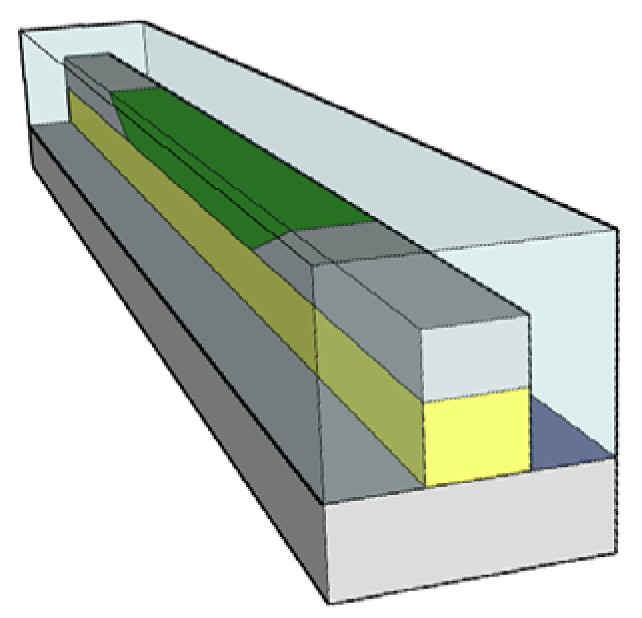
The second important property of that device was that the coupling loss was only 0.6 dB per facet due to excellent mode match to a standard optical fiber. This required an advanced waveguide design. As can be seen from Figures 1 and 2, the typical waveguide mode for the EO polymer waveguide is not symmetric. It can be around 5–6 μm wide and only 2–3 μm high. In comparison with the modes supported by the single mode fibers with the circular cores 10 μm in diameter this would produce significant losses due to the mode mismatch. The design proposed in [11] was based on making hybrid polymer/sol-gel waveguides shown in Figure 3. The waveguide interfacing the input and output fibers were made with sol-gel core and cladding with refractive indices 1.5 and 1.487, respectively. The mode was well-matched with the fibers.
After coupling to the sol-gel core and initial propagation in the sol-gel waveguide the light was adiabatically coupled into the EO polymer (refractive index 1.6–1.7) in the active region of the waveguide, and then back to the sol-gel.
4. Photobleached and e-Beam Bleached Waveguides
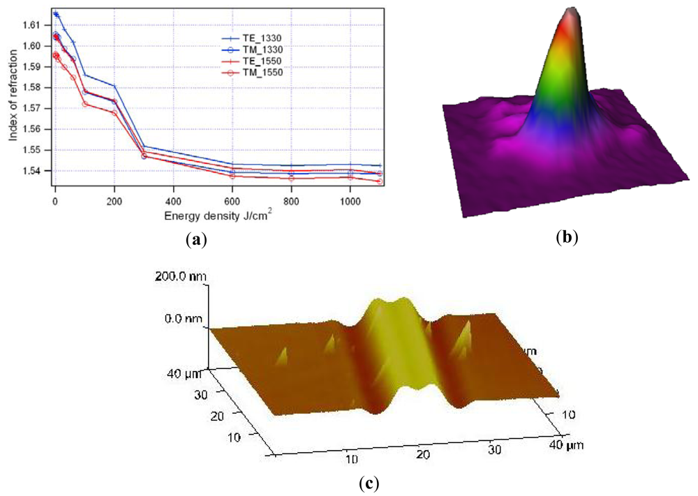
When it is desirable to avoid wet chemicals, such as different solvents and developers, alternative approaches to waveguide patterning have to be used. One such approach is based on bleaching of the EO polymers. Decomposition of the chromophore molecules under direct UV or electron beam irradiation reduces the refractive index of chromophore containing polymers (Figure 4(a)) [12,13]. High energy photons or electrons break the bonds, chromophore molecules decompose and the material color bleaches out. Created refractive index contrast can be ∼0.06–0.07—enough for efficient light guiding. Both photo- and electron-bleaching approaches were used to fabricate high quality microring resonators. The experimentally measured mode propagating in such waveguide is in Figure 4(b).
An interesting aspect of photobleaching is that it's not only changes the refractive index, but also the thickness of the polymer film. Figure 4(c) demonstrates AFM image of the waveguide fabricated using photobleaching with a photolithographic mask. The waveguides were defined as opaque lines on the mask thus being protected from UV radiation. The waveguide surface was directly defined by the diffraction pattern on the photolithographic mask. The height variation was ∼150–200 nm.
5. Field-Induced Waveguides
Local change of refractive index of EO polymer under narrow stripe electrode can be used to create waveguides dynamically (Figure 5). Field-Induced Guiding (FIG) was initially demonstrated in LiNbO3 and GaAs-based heterostructures [14-19]. The advantages of FIG-based design in comparison with traditional designs are temperature and wavelength independence, improved linearity and extremely high bandwidth [20,21]. Wide variety of the devices (light modulators, splitters, scanners, etc.) based on this approach was proposed, but due to high fabrication cost and/or high operation voltages (50–300 V) they were considered impractical. These two problems were solved in the first FIGs in EO polymers demonstrated in [10]. The devices were fabricated from AJL8/APC that was corona poled (EO coefficient r33 ranging from 25 to 31 pm/V) and two sol-gel claddings. The waveguide could be completely turned on by applying 7 volts and switched off by −1 volt. If the latest polymers with 300–500 pm/V were used, the voltage would have decreased proportionally. It was also proposed in [10] that FIG waveguides can be used as building blocks for ultra-flexible reconfigurable systems with dynamic waveguide structure.
6. Slotted Waveguides
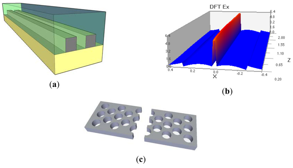
In addition to their excellent EO and photonic properties, EO polymers have great mechanical properties. They can be easily spin-coated on different smooth and patterned surfaces and fill in even very narrow nano-scale slots and nano-holes in photonic crystals. This allows creating waveguides with the width of the guiding mode in order of 100 nm in contrast to several microns typical for all-polymer devices. Furthermore, this greatly improves on-chip integration with silicon photonics and allows creating fast miniature components for on-chip optical interconnects. The schematic view of a silicon slotted waveguide covered with EO polymer is shown in Figure 6(a). The typical mode supported by this waveguide has its maximum in the slot filled with the polymer. Figure 6(c) demonstrates modification of the slotted waveguides fabricated in photonic crystals.
It was experimentally demonstrated that slots as narrow as 75 nm can be infiltrated with EO polymer [7]. However, fabrication of these nano-scale features requires challenging e-beam lithography and reactive ion etching steps. Another important concern is that due to the high leakage current the poling efficiency is decreased and the overall r33 value is only 10–30% compared to the value for EO polymer in thin film. Further improvement can be achieved by decreasing the leakage current. This can be organized by either using EO polymers with lower conductivity or by increasing width of the slot. The latter would decrease separation of electrodes and increase the operating voltage. Optimization study in [6] demonstrated that the optimum slot width is 300–350 nm. For this width 30% of the light still propagates through EO polymer, and the poling can be done efficiently. They also experimentally demonstrated effective in-device r33 of 735 pm/V that was achived in photonic crystal waveguide due to slow light.
Optimization of the slot-waveguide based optical modulators for high speed performance requires additional considerations. The modulator fabricated from a silicon strip-loaded slot waveguide and nonlinear polymer cladding in [5] demonstrated the bandwidth 3 dB-bandwidth of 3 GHz and a VπL figure of merit of 0.8 V·cm. The electrodes were the forming parts of the waveguide, and the driving voltage was applied across a 200 nm slot.
7. Conclusion
In this paper we described several differently designed EO polymer waveguides created taking into considerations a wide range of applications. There are a number of fabrication approaches that can be used depending on the available equipment, material compatibility, and integration with silicon photonics. Furthermore, by picking the right configuration, it is possible to create miniature, ultra-fast and power efficient devices. On the way towards commercialization the main goal is optimization of multiple parameters simultaneously and fabrication of devices demonstrating all these exceptional properties at the same time.


Acknowledgments
A.P. is supported by the National Science Foundation under Grant # 0937060 to the Computing Research Association for the CIFellows Project.
References
- Dalton, L.R.; Robinson, B.; Jen, A.; Ried, P.; Eichinger, B.; Sullivan, P.; Akelaitis, A.; Bale, D.; Haller, M.; Luo, J.; et al. Electro-optic coefficients of 500 pm/V and beyond for organic materials. Proc. SPIE 2005, 5935, 1–12. [Google Scholar]
- Luo, J.; Liu, S.; Haller, M.A.; Kang, J.-W.; Kim, T.-D.; Jang, S.-H.; Chen, B.; Tucker, N.; Li, H.; Tang, H.-Z.; et al. Recent progress in developing highly efficient and thermally stable nonlinear optical polymers for electro-optics. Proc. SPIE 2004, 5351, 36–43. [Google Scholar]
- Dinu, R.; Jin, D.; Yu, G.; Chen, B.; Huang, D.; Chen, H.; Barklund, A.; Miller, E.; Wei, C.; Vemagiri, J. Environmental stress testing of electro-optic polymer modulators. J. Lightwave Technol. 2009, 27, 1527–1532. [Google Scholar]
- Ma, H.; Jen, A.K.; Dalton, L.R. Polymer-based optical waveguides: Materials, processing, and devices. Adv. Mater. 2002, 14, 1339–1365. [Google Scholar]
- Ding, R.; Baehr-Jones, T.; Liu, Y.; Bojko, R.; Witzens, J.; Huang, S.; Luo, J.; Benight, S.; Sullivan, P.; Fedeli, J.-M.; et al. Demonstration of a low VπL modulator with GHz bandwidth based on electro-optic polymer-clad silicon slot waveguides. Opt. Express 2010, 18, 15618–15623. [Google Scholar]
- Wang, X.; Lin, C.-Y.; Chakravarty, S.; Luo, J.; Jen, A.K.; Chen, R.T. Effective in-device r33 of 735 pm/V on electro-optic polymer infiltrated silicon photonic crystal slot waveguides. Opt. Lett. 2011, 36, 882–884. [Google Scholar]
- Lin, C.-Y.; Wang, X.; Chakravarty, S.; Lee, B.S.; Lai, W.; Luo, J.; Jen, A.K.; Chen, R.T. Electro-optic polymer infiltrated silicon photonic crystal slot waveguide modulator with 23 dB slow light enhancement. Appl. Phys. Lett. 2010, 97, 093304. [Google Scholar]
- Shi, Y.; Zhang, C.; Zhang, H.; Bechtel, J.H.; Dalton, L.R.; Robinson, B.H.; Steier, W.H. Low (Sub1-Volt) halfwave voltage polymeric electro-optic modulators achieved by controlling chromophore shape. Science 2000, 288, 119–122. [Google Scholar]
- Sun, H.; Chen, A.; Olbricht, B.C.; Davies, J.A.; Sullivan, P.A.; Liao, Y.; Dalton, L.R. Direct electron beam writing of electro-optic polymer microring resonators. Opt. Express 2008, 16, 6592–6599. [Google Scholar]
- Pyayt, A.; Luo, J.; Jen, A.K.; Dalton, L.; Chen, A. Field-induced guiding optical devices made from electro-optic polymers. Appl. Opt. 2010, 49, 892–896. [Google Scholar]
- Enami, Y.; Derose, C.T.; Mathine, D.; Loychik, C.; Greenlee, C.; Norwood, R.A.; Kim, T.D.; Luo, J.; Tian, Y.; Jen, A.K.; et al. Hybrid polymer/sol-gel waveguide modulators with exceptionally large electro-optic coefficients. Nat. Photonics 2007, 1, 180–185. [Google Scholar]
- Zhou, J.; Pyayt, A.; Dalton, L.R.; Luo, J.; Jen, A.K.; Chen, A. Photobleaching fabrication of microring resonator in a chromophore-containing polymer. IEEE Photonics Technol. Lett. 2006, 18, 2221–2223. [Google Scholar]
- Sun, H.; Chen, A.; Olbricht, B.C.; Davies, J.A.; Sullivan, P.A.; Liao, Y.; Dalton, L.R. Microring resonators fabricated by electron beam bleaching of chromophore doped polymers. Appl. Phys. Lett. 2008, 92, 193305:1–193305:3. [Google Scholar]
- Channin, D.J. Voltage-induced optical waveguide. Appl. Phys. Lett. 1971, 19, 128–130. [Google Scholar]
- Jaeger, N.A.F.; Young, L. Voltage-induced optical waveguide modulator in lithium niobate. IEEE J. Quantum Electron. 1989, 25, 720–728. [Google Scholar]
- Huang, T.-C.; Chung, Y.; Coldren, L.A.; Dagli, N. Field-induced waveguides and their application to modulators. IEEE J. Quantum Electron. 1993, 29, 1131–1143. [Google Scholar]
- Huang, T.C.; Simonis, G.J.; Coldren, L.A. Directional coupler optical switch waveguide. Electron. Lett. 1992, 28, 2422–2435. [Google Scholar]
- Kawakita, Y.; Shimotaya, S.; Machida, D.; Shimomura, K. Wavelength demultiplexing and optical deflection in variable refractive-index waveguide array based on selectively grown GaInAs/InP MQW structure. IEICE Trans. Electron. 2005, E88-C, 1013–1019. [Google Scholar]
- Huang, T.C.; Chung, Y.; Young, D.B.; Dagli, N.; Coldren, L.A. A field induced guide-antiguide modulator on GaAs-AlGaAs. IEEE Photonics Technol. Lett. 1991, 3, 141–143. [Google Scholar]
- Channin, D.J. Voltage-induced optical waveguide. Appl. Phys. Lett. 1971, 19, 128–130. [Google Scholar]
- Jaeger, N.A.F.; Young, L. Voltage-induced optical waveguide modulator in lithium niobate. IEEE J. Quantum Electron. 1989, 25, 720–728. [Google Scholar]
© 2011 by the authors; licensee MDPI, Basel, Switzerland. This article is an open access article distributed under the terms and conditions of the Creative Commons Attribution license (http://creativecommons.org/licenses/by/3.0/).
Share and Cite
Pyayt, A.L. Guiding Light in Electro-Optic Polymers. Polymers 2011, 3, 1591-1599. https://doi.org/10.3390/polym3041591
Pyayt AL. Guiding Light in Electro-Optic Polymers. Polymers. 2011; 3(4):1591-1599. https://doi.org/10.3390/polym3041591
Chicago/Turabian StylePyayt, Anna L. 2011. "Guiding Light in Electro-Optic Polymers" Polymers 3, no. 4: 1591-1599. https://doi.org/10.3390/polym3041591