Injection Compression Molding of Replica Molds for Nanoimprint Lithography

1
Department of Mechanical Engineering, Graduate School of Engineering, The University of Tokyo, 7-3-1 Hongo, Bunkyo-ku, Tokyo 113-8656, Japan
2
Precursory Research for Embryonic Science and Technology (PRESTO), Japan Science and Technology Agency (JST), 4-1-8 Honcho, Kawaguchi, Saitama 332-0012, Japan
Polymers 2014, 6(3), 604-612; https://doi.org/10.3390/polym6030604
Submission received: 3 February 2014
/
Revised: 16 February 2014
/
Accepted: 27 February 2014
/
Published: 5 March 2014
(This article belongs to the Special Issue Patterning and Photosensitive Polymers)
Abstract
:As a breakthrough in the cost and durability of molds for nanoimprint lithography (NIL), replica molds are fabricated by injection compression molding (ICM). ICM is commonly used for optical disks such as DVDs or Blu-ray disks and is also a practical fabrication method for nanostructures. In this paper, I successfully demonstrated the fabrication of cycloolefin polymer replica molds with structures smaller than 60 nm by ICM. Furthermore, ultraviolet (UV)-NIL using these replica molds was demonstrated. UV-cured resist was replicated over an area of 60 mm diameter. The degree of replication by UV-NIL in the first usage of each replica mold had good repeatability. Because ICM is a high-throughput, low-cost process, the replica mold can be disposed of after a certain time for UV-NIL. This method leads to a high-integrity UV-NIL process of patterned media because multiple large-area replica molds can be fabricated simultaneously.
1. Introduction
Since nanoimprint lithography (NIL) was first proposed [1], its practical uses have steadily increased. Because NIL can pattern nanostructured thin resists on substrates without diffraction limitation at a low cost, it is considered to be a viable alternative to optical lithography and electron beam lithography. In particular, the next-generation hard disks, so-called patterned media, are not considered to be practical except if they can be fabricated at low cost [2]. UV-NIL is promising for the high-throughput production of patterns owing to the advantage of room-temperature processing in comparison with thermal NIL [3].
In UV-NIL, a UV transparent mold is pressed into a layer of UV-cured resist on a substrate; UV radiation transmitted through the mold then cures the resist. Quartz molds with nanostructured surfaces are generally used as UV-transparent molds. Patterned quartz molds, however, are too expensive for direct use in practical UV-NIL processes because of the risk of contamination and degradation. Moreover, the quartz molds are rigid, and so, high pressure is required to avoid partial contact distributions when the substrate has some roughness. As a result, the lifetime of a quartz mold is shortened. Replica molding appears to be a solution for this problem. Polymeric materials such as polydimethylsiloxane (PDMS) [4,5], polyvinyl chloride (PVC) [6], polyurethane acrylate (PUA), and polyvinyl alcohol (PVA) have been successfully tested to produce flexible UV-NIL molds.
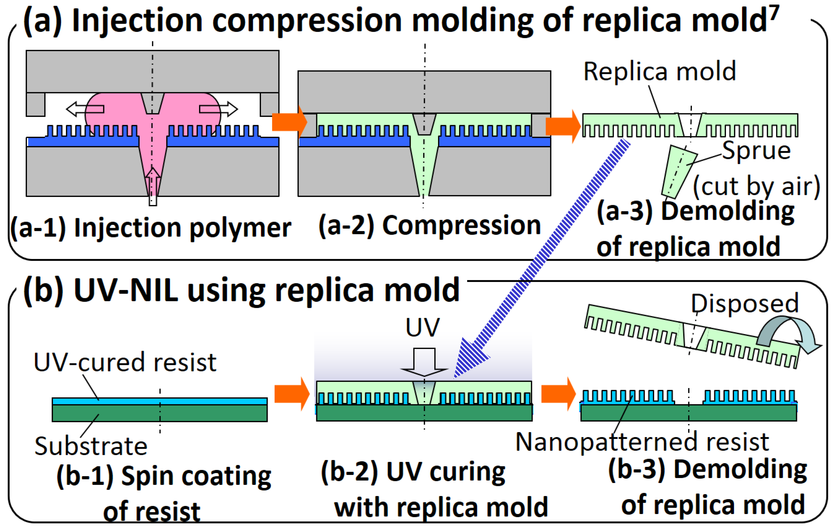
In this paper, I propose and demonstrate the fabrication of replica molds for UV-NIL by injection compression molding (ICM), which is a proven technique for molding optical disks such as compact disks (CDs), digital versatile disks (DVDs), and Blu-ray disks (BDs) with low cost and high throughput [7,8,9]. ICM is one of the lowest cost and highest throughput processes among hot-embossing processes [10,11,12]. Figure 1 shows a schematic of the ICM and UV-NIL processes. The details of the ICM process itself have been described in our previous work [7]. Because ICM has advantages such as low cost, short cycle time, and large area, each replica mold can be used only once, i.e., the replica molds can be disposed of immediately after use for UV-NIL. ICM has another advantage in that melted polymer is injected into the cavity, so the damage due to partial touching is not so critical. Because of this advantage, even though the issue of the Ni-electroplated stamper being used for every replication process still remains, the durability in this case is higher than when the stamper is directly used for NIL.
The basal plates of CDs and BDs are 1.2 mm thick and those of DVDs are 0.6 mm thick. They have a disk shape with an outer diameter of 120 mm and a hole with 15 mm diameter. A 0.3-mm-thick-Ni-electroplated stamper is fixed at the mold bases. To date, our group has demonstrated that polycarbonate (PC) can be replicated to high-aspect-ratio nanostructures with dimensions such as 200 nm width and 400 nm height by ICM [7]. It has not to date been investigated whether structures smaller than 60 nm can be fabricated. Here, I demonstrate the transfer of 60-nm-wide and 60-nm-high patterns using PC and investigate the effect of pattern pitch on the degree of replication. Generally, when the thermal capacity of a replica is low, the solidified layer immediately after the melted polymer touches the mold surface, and the so-called skin layer, becomes thicker. Thus, replication of nanostructures with a replica thickness of 0.6 mm is more difficult than with a thickness of 1.2 mm. In this study, PC was replicated to 1.2 mm thickness, i.e., using mold bases for BDs. On the other hand, the replication of cycloolefin polymer (COP) was demonstrated with 0.6-mm-thick cavity, i.e., using mold bases for DVDs. Furthermore, UV-NIL using the replica molds is demonstrated. Among these two kinds of polymers, COP is considered to be a suitable material for the replica mold because it can be easily replicated by hot embossing and has an anti-stiction property.
Figure 1.
Schematic of ultraviolet nanoimprint lithography (UV-NIL) using an injection-compression-molded replica mold. (a) Injection compression molding (ICM): (a-1) injection of melted polymer, (a-2) polymer is compressed and cooled, and (a-3) replica is demolded and sprue is cut off by an air jet. (b) UV-NIL: (b-1) UV-cured resist is spin-coated onto a substrate; (b-2) replica mold is pressed, UV light is irradiated, resist is cured; and (b-3) replica mold is demolded and disposed of.

2. Experimental Section
Mold replicas were fabricated by ICM with a Ni-electroplated stamper. A Ni stamper had line-and-space patterns with a ridge width of 30 nm, a depth of 58 nm, and pitches of 90 nm, 120 nm, 150 nm, 200 nm, and 320 nm, i.e., trench widths of 60 nm, 90 nm, 120 nm, 170 nm, and 290 nm, respectively. The shape of these patterns has been described in detail in the previous work [13]. The materials used were polycarbonate (PC, AD-5503; Teijin Chemicals Ltd.; glass transition temperature (Tg): 145 °C) and cycloolefin polymer (COP, ZENOR1060R; ZEON CORPORATION; Tg: 100 °C). PC and COP replicas were molded using molds commonly used for BDs and DVDs, respectively. The ICM machine and mold bases used were SD40E of Sumitomo Heavy Industries Ltd., and L-type and U2-type mold bases of SEIKOH GIKEN for the replication of 1.2 mm and 0.6 mm thicknesses, respectively. The Ni-electroplated stamper was set up on both types of mold bases.
The processing conditions for the nine sequential ICM trials are summarized in Table 1. In the ICM experiment using PC and mold base for BDs, the mold temperature, compression pressure, and the temperature of polymer injected at the nozzle were verified to be 80–120 °C, 31–35 MPa, and 350–360 °C, respectively. Note that the mold temperature was indicated to be that of the refrigerant water, and the difference from the temperature of the stamper surface was considered to be less than 5 °C. The compression pressure of 35 MPa is the upper limitation of the machine under these conditions. The temperature of injected polymer, 360 °C, is the upper limitation of the PC. If the PC is heated to above this temperature, the molecules are decomposed. The cycle time was 6 s. During this cycle, the closing mold bases, injection of polymer, opening of mold bases, and pick up were accomplished in 1 s. Compression and cooling were continued for 5 s.

| No. | Polymer | Replica Thickness [mm] | Mold Temperature [°C] | Cycle Time [s] | Cooling Time [s] | Compression Pressure [MPa] | Nozzle Temperature [°C] |
|---|---|---|---|---|---|---|---|
| PC-1 | PC | 1.2 | 90 | 5 | 4 | 31 | 350 |
| PC-2 | ↓ | ↓ | 110 | ↓ | ↓ | ↓ | ↓ |
| PC-3 | ↓ | ↓ | 120 | ↓ | ↓ | ↓ | ↓ |
| PC-4 | ↓ | ↓ | ↓ | ↓ | ↓ | 35 | ↓ |
| PC-5 | ↓ | ↓ | ↓ | ↓ | ↓ | ↓ | 360 |
| COP-1 | COP | 0.6 | 80 | 4 | 3 | 31 | 320 |
| COP-2 | ↓ | ↓ | 90 | 8 | 7 | ↓ | ↓ |
| COP-3 | ↓ | ↓ | 100 | 12 | 11 | ↓ | ↓ |
| COP-4 | ↓ | ↓ | 110→80 | 90 | 32 (80 °C) | ↓ | ↓ |
In the ICM experiments using COP and the DVD mold base, the mold temperature and cycle time were 80 °C, 90 °C, 100 °C, and 110 °C and 4 s, 8 s, 12 s, and 90 s, respectively. In the experiments, the mold temperatures of 80 °C, 90 °C, and 100 °C, were maintained during the processes, and compression and cooling lasted 3 s, 7 s, and 11 s, respectively, as in the experiment using PC. In the experiment with the mold temperature of 110 °C, after injecting polymer, the mold was cooled to 80 °C for 57 s, and the temperature was maintained for 32 s with compression. The reason why the cycle time for higher temperatures was longer than that for lower temperatures is that the complete cooling of the polymer replicated at a higher temperature requires a longer time.
UV-NIL was demonstrated using PC and COP mold replicas that had been fabricated by ICM. UV-cured resist (patent pending) was spin-coated onto a hydrophilically treated 300-mm-diameter silicon substrate, and the replica mold was pressed and UV light was irradiated from the back of the replica mold. The transmission properties of PC and COP in the UV range were confirmed and the UV irradiation time was set accordingly.
The samples of injection-compression-molded replicas, UV-nanoimprinted structures, and replica molds after their use in UV-NIL were examined by atomic force microscopy (AFM, Dimension3100, Veeco, Plainview, NY, USA). The tip used was SSS-NCHR of NANOSENSORS (Spike radius: 3 ± 2 nm, Spike height: 200 nm, Spike tilt: 0 ± 1 nm, Spike ½ angle: 8° ± 2°) and the analyses were carried out in the tapping mode. The investigated patterns were 30 mm from the center of replicas. The pattern height was defined as the average of five peak-to-valley values of the pattern obtained by AFM regardless of their pattern shapes.
3. Results and Discussion
3.1. Injection Compression Molding
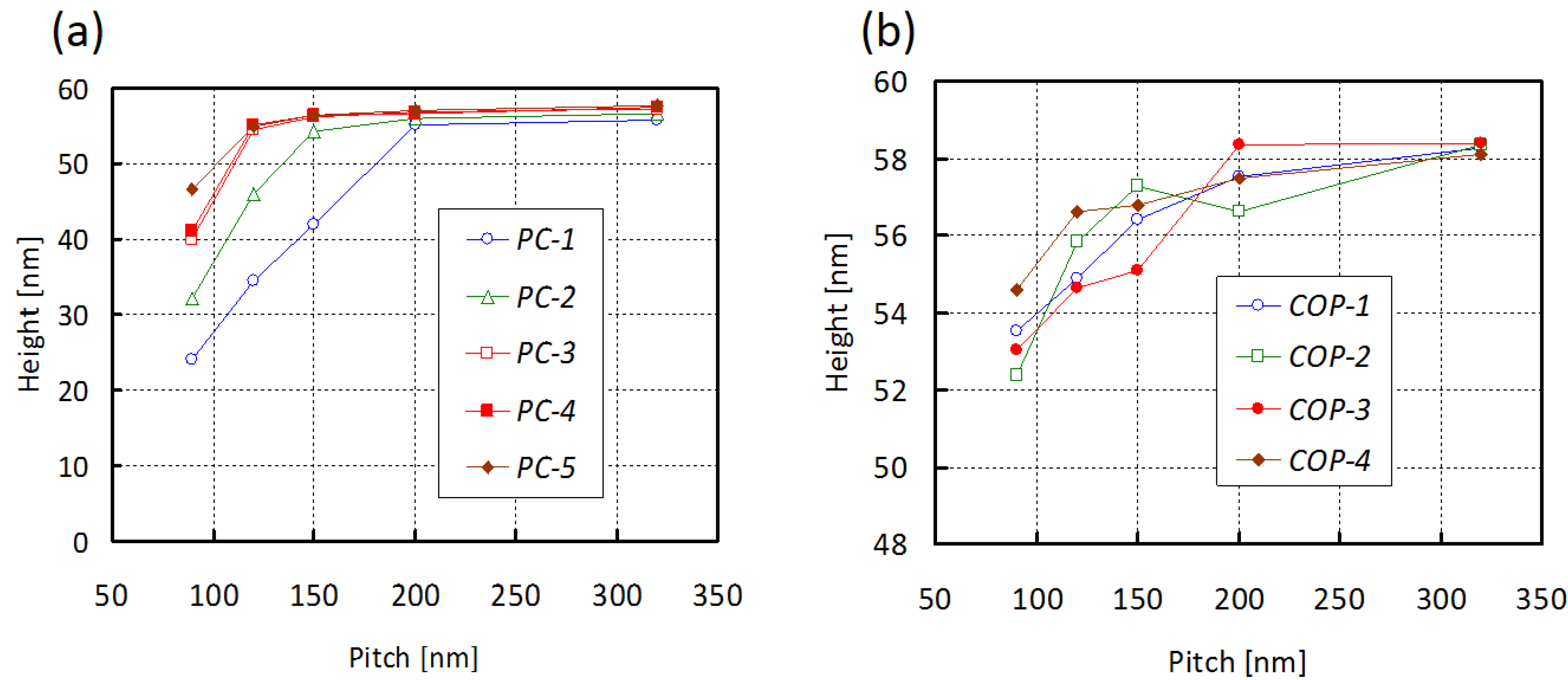
Figure 2 shows a photograph of a replica mold (COP-1). The overviews of all the other replicas were similar to Figure 2. Figure 3a shows heights of replica molds fabricated using PC and BD mold base, obtained from AFM images. First, the replica fabricated with a mold temperature of 90 °C, compression pressure of 31 MPa, and injection temperature of 350 °C (PC-1) had the poorest replication degree. Although the nanostructures with the pitches of 200 nm and 320 nm (cavity widths: 170 nm and 290 nm, respectively) were almost completely replicated, the nanostructures with the pitches of 90 nm, 120 nm, and 150 nm (cavity widths: 60 nm, 90 nm, and 120 nm, respectively) were not, and the structure with the pitch of 90 nm was replicated with less than half the cavity height. Second, when the mold temperature increased to 110 °C, the nanostructure with the pitch of 150 nm was completely replicated (PC-2). Third, when the mold temperature further increased to 120 °C, the nanostructure with the pitch of 120 nm was completely replicated (PC-3). Fourth, when the compression pressure increased to 35 MPa, the degree of replication did not greatly differ from that under the condition of PC-3 (PC-4). Finally, when the injected polymer temperature increased to 360 °C, the degree of replication of the 90-nm-pitch nanostructure was fair, however, the height was approximately 10 nm lower than the cavity height (PC-5).
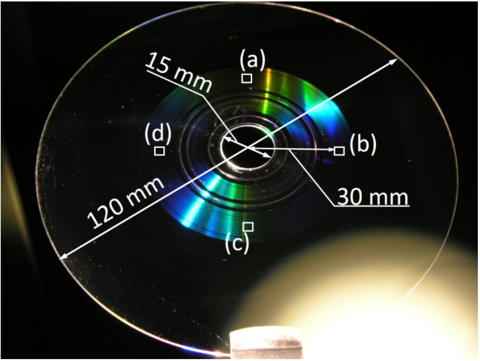
Figure 2.
Photograph of injection-compression-molded replica (this photograph shows a replica mold fabricated under the condition COP-1). Indicated areas 30 mm from the center (a−d) show the regions at which the uniformity of the degree of replication by UV-NIL is examined.
Figure 2.
Photograph of injection-compression-molded replica (this photograph shows a replica mold fabricated under the condition COP-1). Indicated areas 30 mm from the center (a−d) show the regions at which the uniformity of the degree of replication by UV-NIL is examined.

Figure 3.
Pattern heights of injection-compression-molded replicas of samples (a) PC-1-5 and (b) COP-1-4 obtained by atomic force microscopy (AFM) analyses as a function of pattern pitches.
Figure 3.
Pattern heights of injection-compression-molded replicas of samples (a) PC-1-5 and (b) COP-1-4 obtained by atomic force microscopy (AFM) analyses as a function of pattern pitches.

Figure 3b shows pattern heights of replica molds fabricated using COP and DVD molds. Under all conditions, the nanostructures were well replicated; however, the heights of the nanostructures with narrow pitches were 2–6 nm lower than those with wide pitches. Although the temperature of mold bases was higher than Tg (COP-4), the narrower pitch patterns had lower degrees of replication than wider pitch ones. The reason is considered to be that the area of the sidewall with which the Ni stamper is in contact increases as the pattern pitch becomes narrower; thus, the friction forces at the sidewall become higher and the filling progress is stopped when the friction balances with the compression force.
3.2. UV-Nanoimprint Lithography
When UV-NIL was tested using PC replica molds, a UV-cured resist was stuck on the replica molds, and the UV-cured resist was peeled off at the surface of the Si substrate during demolding. The reason is considered to be that PC is a polar molecule and stuck with the UV-cured resist strongly. Therefore, a PC replica mold without any anti-stiction treatment is ineffective for UV-NIL.
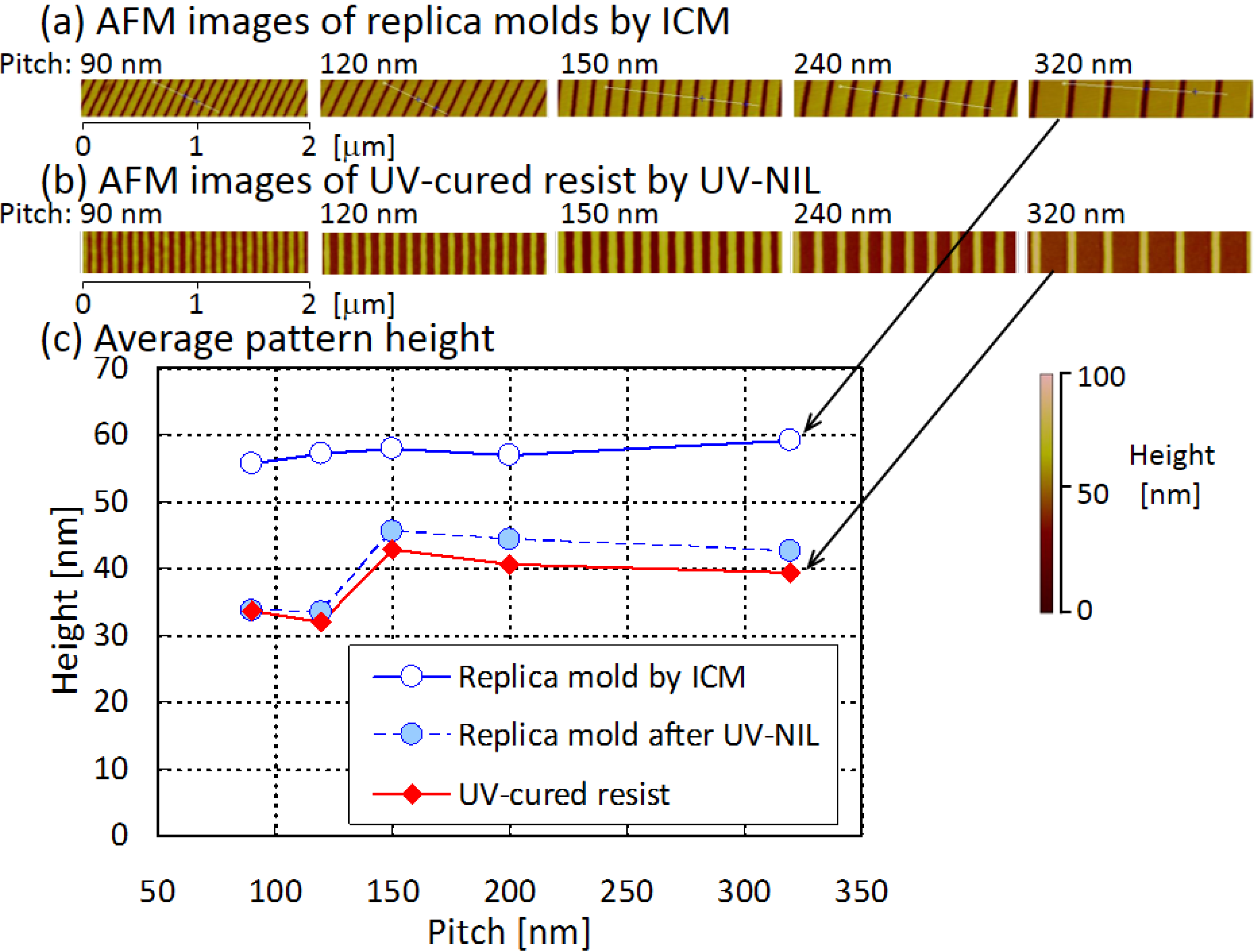
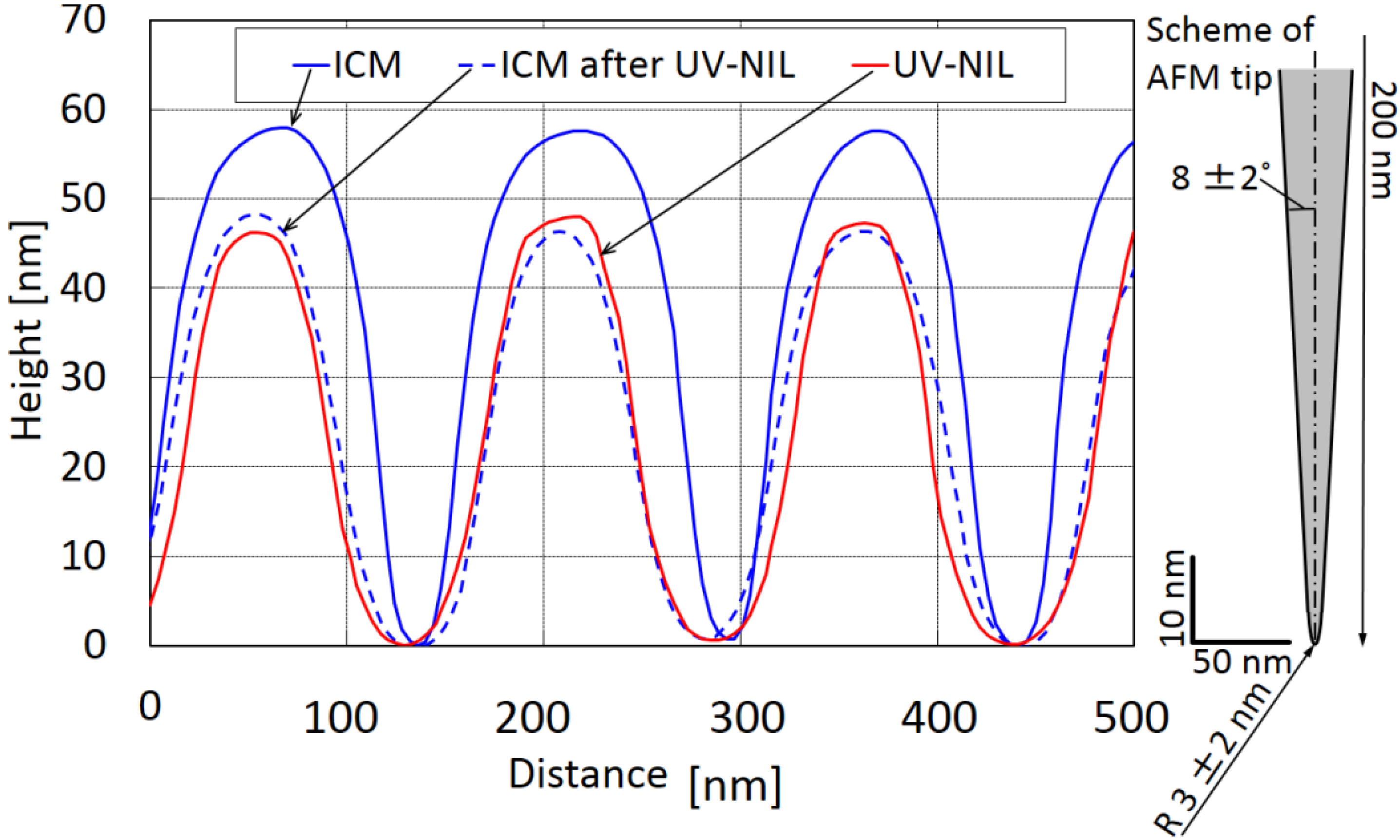
On the other hand, the COP replica mold could be easily demolded after replication by UV-NIL. The main reason for the better demolding characterization should be that COP has no polar character. Figure 4 shows the heights of UV-cured resist nanostructures in comparison with those of replica mold nanostructures. The heights of the sample with pitches of 90 nm, 120 nm, 150 nm, 200 nm, and 320 nm were approximately 34 nm, 32 nm, 43 nm, 41 nm, and 39 nm, respectively. Here, the replica mold after UV-NIL was examined by AFM. The patterns had decreased heights, which corresponds to the UV-cured resist patterns. The degree of pattern transfer in ICM and UV-NIL were investigated by AFM. Figure 5 shows the AFM images of 150-nm-pitch patterns of ICM, ICM after UV-NIL, and UV-cured resist. The result of the UV-cured resist is shown by flipping vertically to compare the shapes easily. The shape of ICM replica decreased not only its height but also width of ridges by UV-NIL. The shape was similar to that of UV-cured resist. From this result, it is considered that the UV-cured resist ridges, which had been cured in the cavity of the replica mold, were separated at their middle because of shrinking during curing or broken during demolding. The height reduction was repeatable.
The height uniformity of the UV-cured resist pattern in the substrate was investigated. The heights at the positions corresponding to Figure 1a–d, that is, the heights of 150-nm-pitch patterns, were 33 nm, 41 nm, 43 nm, and 42 nm, respectively. The height of 33 nm, which corresponds to Figure 1a, was lower than those at other places, because the pressure was insufficient owing to the warpage of the injection-compression-molded replica. In order to solve this problem, the replica should be molded to be a shape with a certain direction of warpage, for example.
Figure 4.
Pattern heights of injection-compression-molded replica (sample COP-1), after use in UV-NIL, and UV-cured resist, obtained by AFM analyses as a function of pattern pitch.
Figure 4.
Pattern heights of injection-compression-molded replica (sample COP-1), after use in UV-NIL, and UV-cured resist, obtained by AFM analyses as a function of pattern pitch.

Figure 5.
AFM images of the 150-nm-pitch patterns of injection-compression-molded replica (sample COP-1), after use in UV-NIL, and UV-cured resist. The scheme of AFM tip used is illustrated with the same scale of the graph.
Figure 5.
AFM images of the 150-nm-pitch patterns of injection-compression-molded replica (sample COP-1), after use in UV-NIL, and UV-cured resist. The scheme of AFM tip used is illustrated with the same scale of the graph.

4. Conclusions
I have proposed the use of a replica mold reproduced by injection compression molding in UV-nanoimprint lithography. Using the pattern of 60-nm-wide cavities, PC and COP were replicated. The PC replica cannot be demolded from UV-cured resist and is not useful for UV-NIL without anti-stiction treatment. On the other hand, COP replica was successfully used in the UV-NIL process. This is because PC polarizes and sticks UV-cured resist and COP does not and was easily demolded. UV-cured resist ridges, which had been cured in the cavity of the replica mold, were considered to be separated at their middle because of shrinking during curing or were broken due to friction during demolding.
Acknowledgments
The masters of the Ni electroplated molds were provided and the AFM analyses were carried out by Mr. Ichikawa at Fujifilm Corporation. The injection compression molding experiments were carried out by Mr. Oike at SEIKO GIKEN. This work was partially supported by a Grant-in-Aid for Scientific Research (No. 19106003) from the Ministry of Education, Culture, Sports, Science and Technology, Japan.
Conflicts of Interest
The author declares no conflict of interest.
References
- Chou, S.Y.; Krauss, P.R.; Renstrom, P.J. Imprint of sub-25 nm vias and trenches in polymers. Appl. Phys. Lett. 1995, 67, 3114–3116. [Google Scholar] [CrossRef]
- Kaizu, A.; Soeno, Y.; Tagami, K. Effect of discrete track medium at high areal density. J. Magnet. Magn. Mater. 2008, 320, 3161–3164. [Google Scholar] [CrossRef]
- Haisma, J.; Verheijen, M.; van den Heuvel, K.; van den Berg, J. Mold-assisted nanolithography: A progress for reliable pattern replication. J. Vac. Sci. Technol. B 1996, 14, 4124–4128. [Google Scholar] [CrossRef]
- Gilles, S.; Meier, M.; Prömpers, M.; can der Hart, C.; Kügeler, C.; Offenhäuser, A.; Mayer, D. UV nanoimprint lithography with rigid polymer molds. Microelectron. Eng. 2009, 86, 661–664. [Google Scholar] [CrossRef]
- Plachetka, U.; Bender, M.; Fuchs, A.; Vratzov, B.; Glinsner, T.; Lindner, F.; Kurz, H. Wafer scale patterning by soft UV-Nanoimprint Lithography. Microelectron. Eng. 2004, 73–74, 167–171. [Google Scholar] [CrossRef]
- Koo, N.; Bender, M.; Plachetka, U.; Fuchs, A.; Wahlbrink, T.; Bolten, J.; Kurz, J. Improved mold fabrication for the definition of high quality nanopatterns by Soft UV-Nanoimprint lithography using diluted PDMS material. Microelectron. Eng. 2007, 84, 904–908. [Google Scholar] [CrossRef]
- Nagato, K.; Hamaguchi, T.; Nakao, M. Injection compression molding of high-aspect-ratio nanostructures. J. Vac. Sci. Technol. B 2011, 29. [Google Scholar] [CrossRef]
- Ohta, T.; Inoue, K.; Ishida, T.; Gotoh, Y.; Satoh, I. Thin injection-molded substrate for high density recording phase-change rewritable disk. Jpn. J. Appl. Phys. 1993, 32, 5214–5218. [Google Scholar] [CrossRef]
- Imai, T.; Shida, N.; Higuchi, T.; Suga, K.; Iida, T.; Yokogawa, F. 25 Gbyte read-only memory disk by injection-compression molding process. Jpn. J. Appl. Phys. 2001, 40, 1661–1665. [Google Scholar] [CrossRef]
- Schift, H.; David, C.; Gabrecht, M.; Heyderman, L.J.; Kaiser, W.; Koppel, S.; Scandella, L. Nanoreplication in polymers using hot embossing and injection molding. Microelectron. Eng. 2000, 53, 171–174. [Google Scholar] [CrossRef]
- Su, Y.C.; Shah, J.; Lin, L. Implementation and analysis of polymeric microstructure replication by micro injection molding. J. Micromech. Microeng. 2004, 14, 415–422. [Google Scholar] [CrossRef]
- Ting, C.J.; Huang, N.C.; Tsai, H.Y.; Chou, C.P.; Fu, C.C. Low cost fabrication of the large-area anti-reflection films from polymer by nanoimprint/hot-embossing technology. Nanotechnology 2008, 19. [Google Scholar] [CrossRef]
- Ichikawa, K.; Usa, T.; Nishimaki, K.; Usuki, K. Design of Ni mold for discrete track media. IEEE Trans. Magn. 2008, 40, 3450–3453. [Google Scholar] [CrossRef]
© 2014 by the authors; licensee MDPI, Basel, Switzerland. This article is an open access article distributed under the terms and conditions of the Creative Commons Attribution license (http://creativecommons.org/licenses/by/3.0/).
Share and Cite
MDPI and ACS Style
Nagato, K. Injection Compression Molding of Replica Molds for Nanoimprint Lithography. Polymers 2014, 6, 604-612. https://doi.org/10.3390/polym6030604
AMA Style
Nagato K. Injection Compression Molding of Replica Molds for Nanoimprint Lithography. Polymers. 2014; 6(3):604-612. https://doi.org/10.3390/polym6030604
Chicago/Turabian StyleNagato, Keisuke. 2014. "Injection Compression Molding of Replica Molds for Nanoimprint Lithography" Polymers 6, no. 3: 604-612. https://doi.org/10.3390/polym6030604