Review

Organic Semiconductor/Insulator Polymer Blends for High-Performance Organic Transistors

1
Department of Organic and Nano System Engineering, Konkuk University, Seoul 143-701, Korea
2
Department of Energy and Chemical Engineering, Incheon National University, Incheon 406-772, Korea
*
Authors to whom correspondence should be addressed.
Polymers 2014, 6(4), 1057-1073; https://doi.org/10.3390/polym6041057
Submission received: 11 February 2014 / Revised: 24 March 2014 / Accepted: 31 March 2014 / Published: 8 April 2014
(This article belongs to the Special Issue Semiconducting Polymers for Organic Electronic Devices)

Abstract

:
We reviewed recent advances in high-performance organic field-effect transistors (OFETs) based on organic semiconductor/insulator polymer blends. Fundamental aspects of phase separation in binary blends are discussed with special attention to phase-separated microstructures. Strategies for constructing semiconductor, semiconductor/dielectric, or semiconductor/passivation layers in OFETs by blending organic semiconductors with an insulating polymer are discussed. Representative studies that utilized such blended films in the following categories are covered: vertical phase-separation, processing additives, embedded semiconductor nanowires.

1. Introduction

Organic field-effect transistors (OFETs) have received much attention as switching elements in display backplanes [1,2,3,4,5,6,7,8,9,10,11,12,13,14]. The electrical performance of OFETs is now comparable or exceeds that of amorphous Si: H FETs. For example, high field-effect mobilities >10 cm2/Vs were recently reported for polymer-based FETs [15,16]. These polymer semiconductors are attractive materials, as a polymer can be deposited through an easy solution process. The solution process is advantageous for scale-up while minimizing processing costs. Printing processes such as the roll-to-roll process can be utilized to mass produce OFETs, and prototype devices have been demonstrated [3]. If environmental and electrical stabilities are supplemented, OFETs can be used to enable flexible/stretchable electronics [1]. If low stability is a critical drawback for commercialization of OFETs, OFETs may be used in disposable electronics. To achieve this goal, the solution process is indispensable for reducing processing costs.
Another important advantage of a solution process comes from versatility in the selection of materials. Various materials with different functions can be blended to fine tune device performance. This blended approach is common when preparing active layers in organic photovoltaic solar cells (OPVs) or ambipolar FETs [17,18,19,20]. In such devices, device performance is typically determined by phase-separation characteristics in n-type semiconductor/p-type semiconductor polymer blends. The movements of the hole and electron carriers are regulated by fine tuning phase-separation. In contrast, insulating materials have been added to construct OPV and OFET active layers. Such materials in OPVs induce slow evaporation of solvent, thereby increasing crystallinity of the organic semiconductors. The added insulating materials are typically small molecules with high boiling points. If an insulator polymer is added to the organic semiconductor of an OFET, the added insulator polymer prohibits transport of charge carriers [21]. Thus, a rational and straight-forward method to avoid this problem is to guarantee the current pathway by appropriate phase separation.
In this review article, representative studies that utilize organic semiconductor/insulator polymer blends for high-performance OFETs are introduced. In Section 2, the fundamental aspects of phase separation are discussed. In Section 3, representative studies that used organic semiconductor/insulator polymer blends are introduced with special attention to the strategies for maintaining the percolation path and utilizing an insulator polymer in OFETs. Finally, a brief summary is provided in the conclusion section.

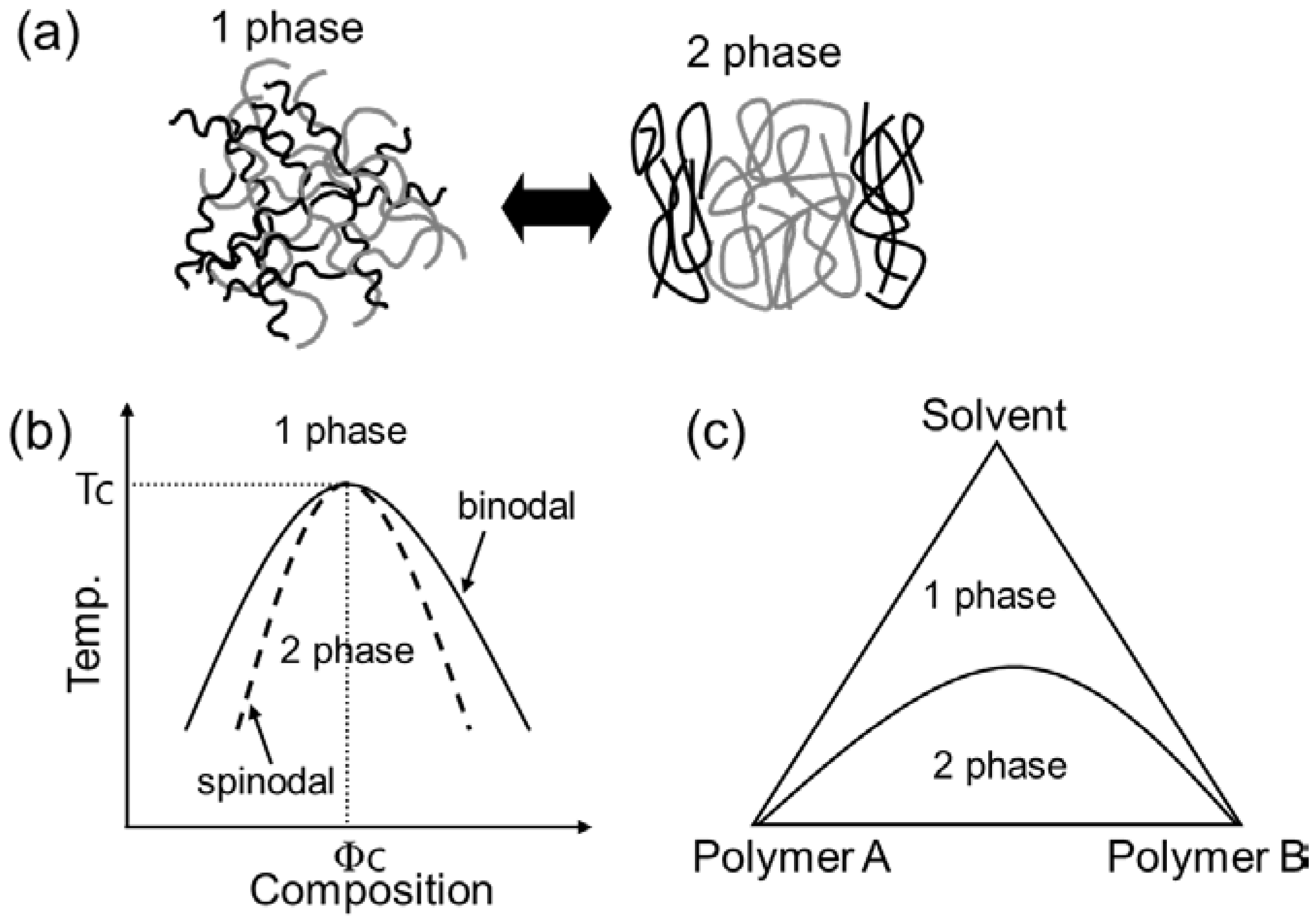
2. Fundamental Aspects of Phase Separation

Phase separation is a complex phenomenon that depends on molecular parameters (i.e., miscibility of two polymers, concentration, and solvent), thermodynamic parameters (i.e., composition, temperature, and pressure) and processing parameters (i.e., film deposition method). Figure 1a is a schematic of the phase-separation characteristic of a binary polymer blend. During solvent evaporation, the blend changes from one mixed phase to two individual phases. Phase-separation behaviors are dependent on the free energy G of the system from a thermodynamic point of view [4]. The borderline of phase separation is divided into two categories: spinodal (∂G2/∂c2 = 0) and binodal (∂G/∂c = 0) lines. Figure 2b shows the spinodal and binodal lines of a binary polymer blend as a function of composition and temperature. When temperature is high, entropy is a governing factor and, thus, one mixed phase is favored. Two individual phases are preferred by enthalpic interaction when the temperature decreases [22]. In addition, composition c has a significant impact on determining the borderlines of the phase separation (Figure 2b). Because a solvent is typically used to make a blended solution, a ternary system consisting of polymer A, polymer B, and the solvent is considered (Figure 2c). When the solvent evaporates, two different phase-separation modes exist: spinodal decomposition and nucleation and growth. Lateral or vertical phase separation is strongly dependent on the mode the blend solution goes through.
Figure 1. (a) Phase separation characteristics of a binary polymer blend; (b) Spinodal and binodal lines of a binary polymer blend as a function of composition and temperature; (c) A ternary phase diagram for the system with polymer A, polymer B, and the solvent.
Polymers 06 01057 g001
Polymer, solvent, substrate, and processing conditions mutually affect phase-separation characteristics. Miscibility is an important polymer property, which is commonly determined by considering the Flory-Huggins interaction parameter (χ). A high χ value means a strong driving force for phase separation. In addition, composition, molecular weight, and concentration of the solution are important properties. The solvent evaporation rate is commonly influenced by the choice of solvent with a different boiling point. The time for phase separation is long if a solvent with a high boiling point is used. Surface tension and viscosity of the solution is also determined by solvent choice. If the solubilities of two polymers are different, the polymer with the lowest solubility solidifies first. Thus, solubility is an important parameter that determines structure of vertical phase separation. The surface energy of the substrate is important when the solution solidifies on the substrate. First, it affects wetting properties when solution droplets form. Surface energy governs the formation of the transient wetting layer during solvent evaporation. Finally, the phase-separated structure is determined by the subtle change in surface energy and roughness of the substrate. Processing conditions such as spin speed during spin casting strongly affect the phase-separation kinetics. In one study, vertical phase-separation occurred under a specific spin speed of spin-casted polymer blends [23]. Because of a preference for vertically phase-separated polymer blends, many researchers have tried to fabricate vertically phase-separated structures using polymer blends [21]. However, vertically phase-separated structures can be obtained under specific molecular and processing conditions. This is due to Marangoni-like instability during solvent evaporation. Heriot et al., revealed that the vertically phase-separated transient layer becomes unstable and that the final film morphology adopts a laterally phase-separated structure during spin casting of polymer blends [24]. When polymer blends are used to construct layers in OFETs, these fundamental aspects of phase separation should be considered to obtain an appropriate phase-separated structure. For example, a vertically phase-separated structure in organic semiconductor/insulator polymer blends can be used as an active layer in OFETs and this can be achieved by controlling solubility, surface energy, and/or substrate conditions.

3. Organic Semiconductor/Insulating Polymer Blends

Figure 2 shows the schematic layered structures of OFETs consisting of substrate, gate-electrode, dielectric, semiconductor, source/drain electrodes, and the passivation layer. Gate-electrode, dielectric, semiconductor, and source/drain electrodes are included between the passivation layer and the substrate. According to the relative location of the gate-electrode and source/drain electrodes, OFETs are classified into four types: (a) bottom-gate/bottom-contact (coplanar), (b) bottom-gate/top-contact (staggered), (c) top-gate/bottom-contact (staggered), and (d) top-gate/top-contact (coplanar) [25]. Regardless of the type of OFET structure, charge carriers accumulate at the semiconducting layer near the dielectric layer after bias at the gate electrode [26]. These accumulated charge carriers pass through from the source to the drain electrode due to the potential difference between the two electrodes. An active channel region in each device structure, which corresponds to the charge transport pathway, is indicated in red. In coplanar types, source/drain electrodes are placed in the same line with the charge transport pathways. In contrast, source/drain electrodes are not placed in a horizontal line with the charge transport pathway in the staggered type, and injected charge carriers should transport vertically to arrive in the active channel region. The passivation layer is commonly used to protect organic semiconductors from O2 and/or H2O under ambient conditions. Note that an organic semiconductor is vulnerable to O2 and/or H2O molecules and, accordingly, device performance degrades significantly with time [1]. The passivation layer is indispensable in the bottom-gate structure because the semiconducting layer is directly exposed to ambient air (Figure 2a,b). However, the dielectric layer protects the semiconducting layer in the top-gate structure (Figure 2c,d); thus, the choice of a passivation layer is optional.
Organic semiconductor-top/insulator polymer-bottom or insulator polymer-top/organic semiconductor-bottom bilayer structures can be induced through vertical phase-separation of organic semiconductor/insulator polymer blends. Device structure should be considered for possible uses of organic semiconductor/insulator polymer blends in OFETs. The passivation layer and semiconductor can be simultaneously deposited in a bottom-gate/bottom-contact structure (Figure 2a) by inducing an insulator polymer-top/organic semiconductor-bottom vertically phase-separated structure. This phase-separated structure can be alternatively used to simultaneously fabricate a dielectric and semiconductor in a top-gate/bottom-contact device structure (Figure 2c). However, an organic semiconductor-top/insulator polymer-bottom vertically phase-separated structure is useful to fabricate both a semiconductor and dielectric in the bottom-gate/top-contact structure (Figure 2b). The staggered type is more preferable than the coplanar type when fabricating a semiconductor and dielectric together using polymer blends because the phase-separated interface can be directly used as the charge transport pathway (compare devices in Figure 2b,c) with those in Figure 2a,d.
Figure 2. Schematic layered structures of organic field-effect transistors (OFETs): (a) bottom-gate/bottom-contact (coplanar); (b) bottom-gate/top-contact (staggered); (c) top-gate/bottom-contact (staggered); (d) top-gate/top-contact (coplanar).
Polymers 06 01057 g002

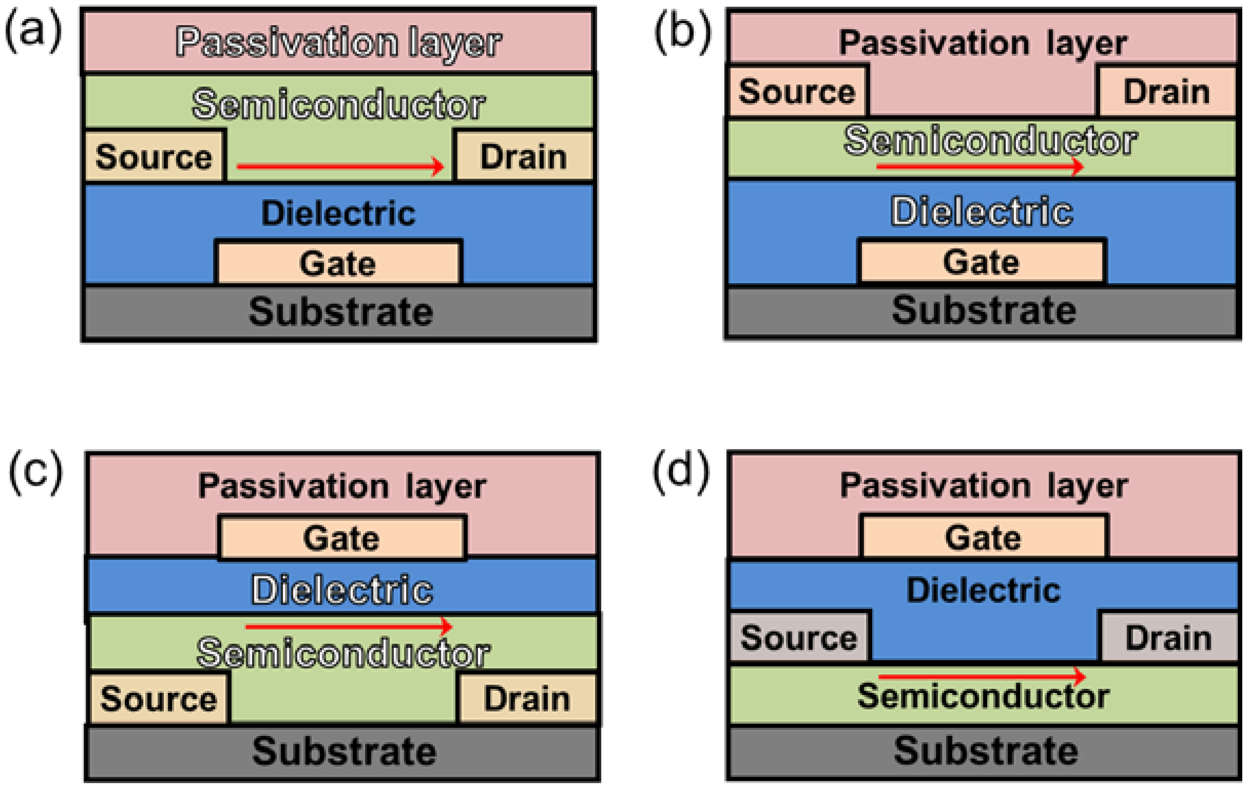
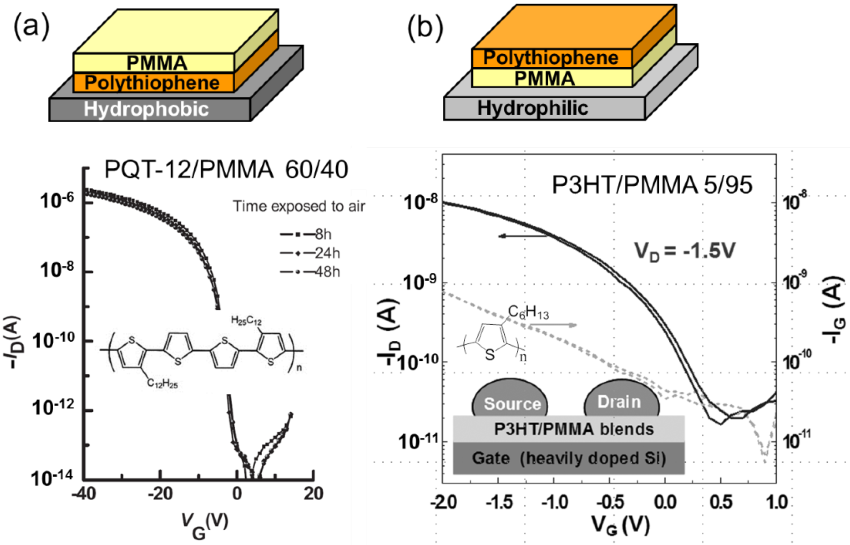
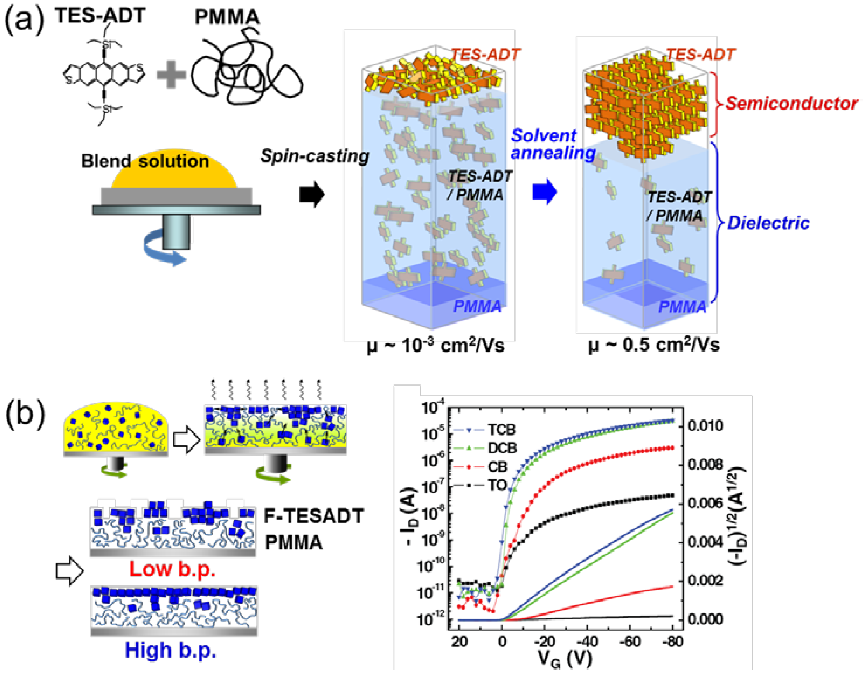
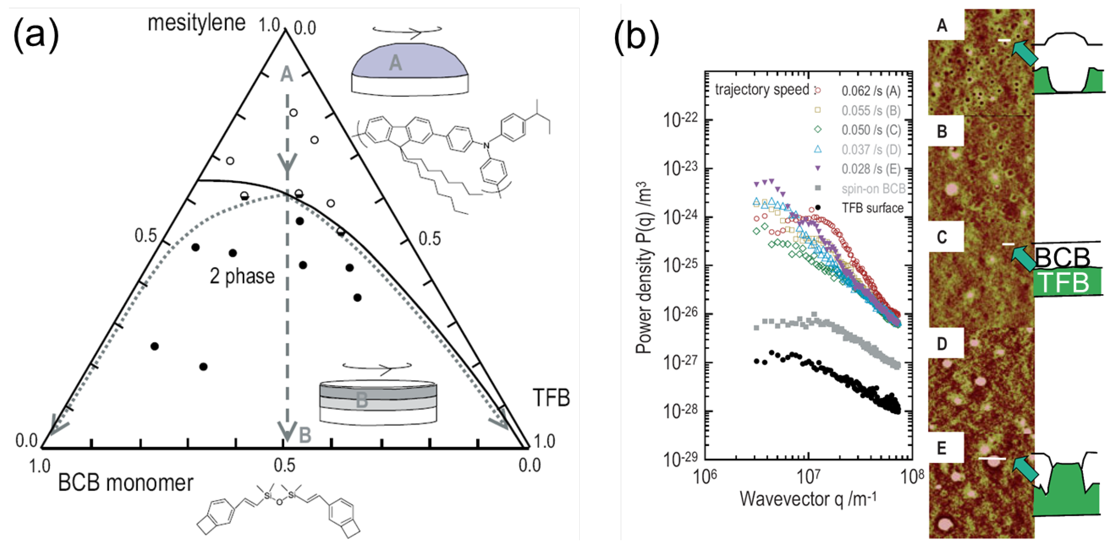
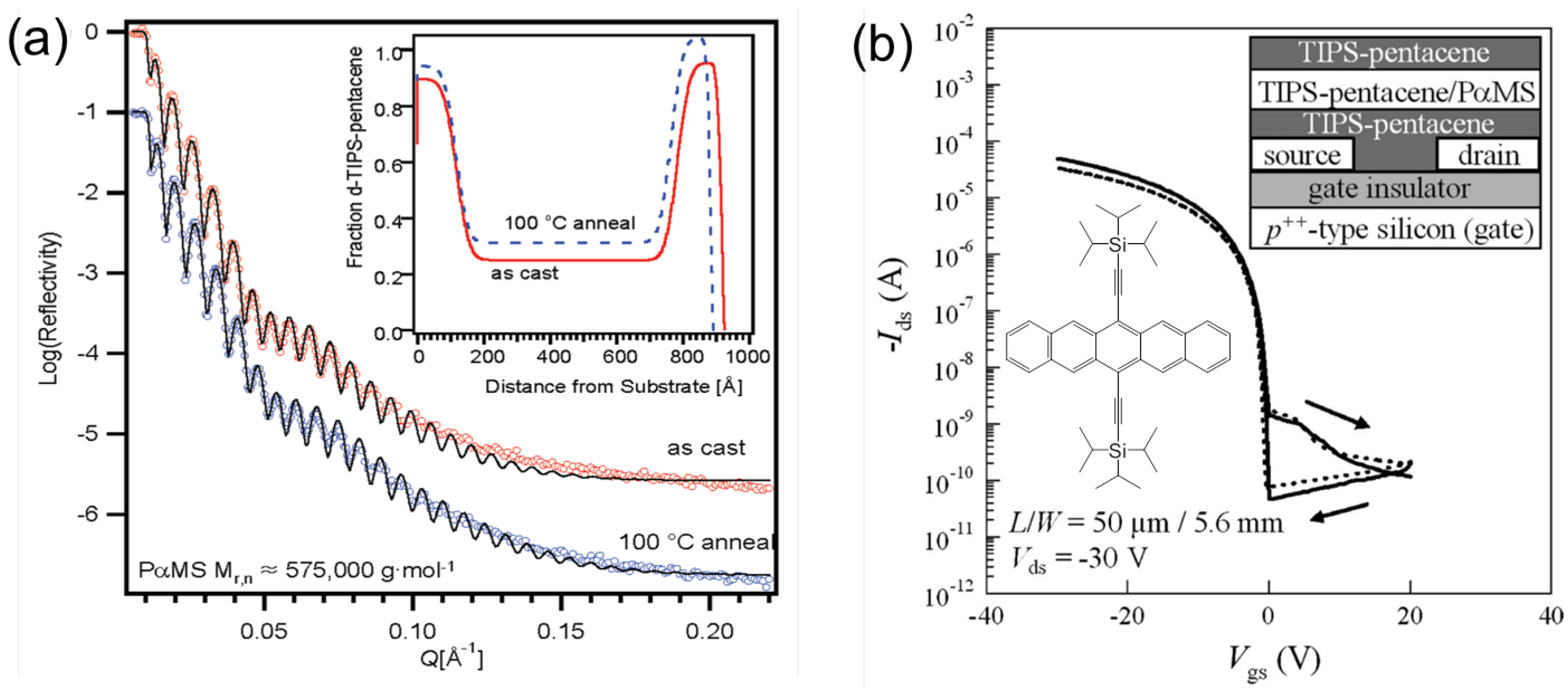
3.1. Vertical Phase-Separation

Vertical phase separation is a rational route to fabricate dual layers in OFETs [4]. Organic semiconductor/insulator polymer blends can provide both a semiconducting layer and a passivation layer (or dielectric layer) [27]. Although similar polymer blend pairs are used, phase-separation characteristics differ with use of a different substrate. Figure 3 shows the schematic phase-separation characteristics of polythiophene/poly(methyl methacrylate) (PMMA) blends. On a hydrophobic substrate, polythiophene with low surface tension is preferentially deposited on the film-substrate interface. Arias et al., found that a PMMA-top/poly[5,5′-bis(3-dodecyl-2-thienyl)-2,2′-bithiophene)] (PQT-12)-bottom bilayer structure forms spontaneously on an octyltrichlorosilane (OTS-8) treated SiO2/Si substrate by phase separation of the PQT-12: PMMA blend (Figure 3a) [28]. They explained this phenomenon by introducing the concept of spreading pressure. The spreading pressure of the PMMA solution is lower than that of PQT-12 on a hydrophobic OTS-8 treated SiO2/Si substrate. Thus, energy minimization leads to the formation of PMMA-top/PQT-12-bottom bilayer structure. Figure 3a shows the time-dependent electrical properties of OFETs based on a PQT-12: PMMA blended film. OFETs exhibit unchanged electrical properties following over exposure to ambient air during 48 h. Because PMMA on top can be used as a passivation layer in OFETs (Figure 2a), OFETs based on PQT-12: PMMA blended film exhibit higher environmental stability than those of OFETs based on PQT-12 film.
In contrast, PMMA with high surface tension on a hydrophilic substrate is deposited on the film-substrate interface, whereas polythiophene, with low surface energy, is placed on the air-film interface. Figure 3b shows the electrical properties of OFETs based on a poly(3-hexylthiophene) (P3HT): PMMA blended film where phase-separated P3HT at the air-film interface serves as a semiconducting layer and phase-separated PMMA at the film-substrate interface serves as a dielectric layer (Figure 2b) [29]. Remarkably, P3HT content in a P3HT:PMMA blend was reduced down to 2% without compromising the electrical properties. Thus, this approach is useful to reduce semiconductor content in OFETs, thereby reducing material costs. Low voltage driven OFETs have been successfully fabricated because a phase-separated thin PMMA layer can work as a gate dielectric (Figure 3b). Wang et al., examined the effect of film processing conditions (i.e., solution concentration) on the morphology of the phase-separated interface between P3HT and PMMA [30]. A higher solution concentration tended to decrease roughness of the phase-separated interface. This, in turn, enhanced the electrical properties of the OFETs because the phase-separated interface served as a pathway for charge transport (Figure 2b), and the smooth interface is beneficial for facilitating efficient charge transport.
Figure 3. Vertical phase-separation in polythiophene: poly(methyl methacrylate) (PMMA) blended films: (a) PMMA-top/polythiophene-bottom structure and electrical property of the organic field-effect transistor (OFET) based on PMMA-top/poly[5,5′-bis(3-dodecyl-2-thienyl)-2,2′-bithiophene)] (PQT-12)-bottom blend film. Reproduced from [24]. Copyright 2006 Wiley. (b) Polythiophene-top/PMMA-bottom structure and electrical properties of an OFET based on poly(3-hexylthiophene) (P3HT)-top/PMMA-bottom blended film. Chemical Structures of PQT-12 and P3HT are shown in the inset. Reproduced from [25]. Copyright 2008 Wiley.
Polymers 06 01057 g003
Soluble acenes are advantageous organic semiconductors because materials with solution processability and high π-orbital overlaps have been reported [31,32,33]. Where this type of organic semiconductor is used, processing conditions should be optimized to obtain desirable thin film morphologies and microstructures, thereby maximizing the electrical properties of OFETs. For example, field-effect mobilities can differ over several orders by using different processing conditions [31,34]. Soluble acene/insulating polymer blends are interesting building blocks to fabricate OFET layers [35,36]. When a soluble acene/PMMA blend is deposited on a hydrophilic substrate, the soluble acene with low surface energy is preferentially deposited at the air-film interface (Figure 4a) [37]. This is due to the surface energy differences between soluble acene and PMMA. A blended film consisting of a soluble acene-top layer and a PMMA-bottom layer can be utilized to fabricate both semiconductors and dielectrics (Figure 2b). Lee et al., used a 5,11-bis(triethylsilylethynyl) anthradithiophene (TES-ADT): PMMA blend to fabricate a TES-ADT-top/PMMA-bottom bilayer structure [37]. After spin casting the blended solution, TES-ADT with low surface energy was deposited on the air-film interface, whereas PMMA with high surface energy was deposited on the film-substrate interface. However, TES-ADT molecules remained on the PMMA layer as a result of fast solvent evaporation during spin casting. After solvent vapor annealing with 1,2-dichloroethane, the TES-ADT molecules move up to minimize total surface energy of the blended film. Accordingly, vertical phase separation is greatly enhanced. In addition, TES-ADT molecules crystallize under the solvent-vapor environment; thus, adopting three-dimensional multilayered structures, which are extremely beneficial for lateral transport of charge carriers [38,39,40]. The average field-effect mobility of OFETs based on TES-ADT: PMMA blended film increases from 10−3 to 0.5 cm2/Vs after solvent vapor annealing. This is due to the combined effect of enhanced vertical phase separation and crystallization of TES-ADT after solvent vapor annealing.
Figure 4. (a) Schematic representations of the morphological and structural characteristics of 5,11-bis(triethylsilylethynyl) anthradithiophene (TES-ADT): PMMA blended films after spin-casting and solvent-vapor annealing. Field-effect mobilities of the organic field-effect transistors (OFETs) based on the blended films are shown at the bottom of the schemes. Reproduced from [30]. Copyright 2009 Wiley; (b) Schematic representations of the morphological and structural characteristics in 2,8-difluoro-5,11-bis(triethylsilylethynyl) anthradithiophene (F-TESADT): PMMA blended films spin-cast from various solvents (low b.p.: low boiling point solvent; high b.p.: high boiling point solvent). Electrical properties of OFETs based on the blended films prepared with various solvents are also shown (TO: toluene, CB: chlorobenzene, DCB: 1,2-dichlorobenzene, TCB: 1,2,4-trichlorobenzene). Reproduced from [34]. Copyright 2012 Wiley.
Polymers 06 01057 g004
Although solvent vapor annealing is an effective method to induce phase separation of a blended film and crystallization of soluble acene, the practical application is limited by use of a harmful solvent. It is much more desirable if a soluble acene-top/insulating polymer-bottom bilayer structure can be obtained by spin casting. Lee et al., used a 2,8-difluoro-5,11-bis(triethylsilylethynyl) anthradithiophene (F-TESADT): PMMA blend to induce vertical phase separation using a one-step spin-casting process (Figure 4b) [41]. Because fluorine atoms in F-TESADT reduced surface tension of the F-TESADT molecule, F-TESADT molecules were effectively crystallized at the air-film interface during phase separation with PMMA. In addition, crystallization of F-TESADT was enhanced by fluorine-fluorine interactions between F-TESADT molecules [42]. However, the phase-separation characteristics between F-TESADT and PMMA and crystallization of F-TESADT are largely dependent on the selection of solvent for preparing the blended solution. If a solvent with a low boiling point (b.p.) is used, the solvent evaporation rate is fast. Accordingly, vertical phase separation is not perfectly attained. In contrast, using a solvent with a high b.p. imparts enough time to accomplish vertical phase separation. The F-TESADT molecules at the air-film interface crystallize and grow into large crystals. Thus, an F-TESADT crystal-top/PMMA-bottom bilayer structure was successfully fabricated with a spin-casting blended solution with a high b.p. Average field-effect mobility of OFETs based on blended film increases when the b.p. of the solvent used increases (Figure 4b right). In addition, environmental and electrical stabilities of OFETs based on F-TESADT: PMMA blended films are far superior to those of OFETs based on homo F-TESADT film. These enhanced stabilities are due to the unique structure of OFETs consisting of highly crystallized F-TESADT crystals (top) and trap-minimized PMMA (bottom).
We introduced the use of organic semiconductor/insulator polymer blends in bottom-gate OFETs. When top-gate OFETs are used, phase-separation characteristics should be different for applying blended materials. As schematically shown in Figure 2c, insulator polymer-top/organic semiconductor-bottom blended film can be utilized to simultaneously fabricate semiconductors and dielectrics. Chua et al., succeeded in fabricating a divinyl-tetramethyldisiloxane-bis(benzocyclobutene) (BCB)-top/poly(9,9-dialkylfluorone-alt-triarylamine) (TFB)-bottom bilayered structure by spin casting a BCB: TFB blended solution in mesitylene [23]. Figure 5a shows a ternary phase diagram of the BCB: TFB: mesitylene system. Because solvent is rich at point A, the solution exists as a single phase as marked by the white circle. When the solvent evaporates, the BCB-TFB-mesitylene solution passes through binary systems consisting of BCB-mesitylene and TFB-mesitylene. Finally, a vertically phase-separated BCB-top/TFB-bottom bilayer structure was obtained (point B). Because the surface tension of BCB is higher than that of TFB, BCB is segregated at the air-film interface. In addition, a high Flory-Huggins interaction parameter (e.g., χBCB/TFB = 3) accelerates phase separation between BCB and TFB.
Although formation of a BCB-top/TFB-bottom bilayer structure is thermodynamically driven, the detailed phase-separated morphology is dependent on the solvent evaporation rate. The solvent evaporation rate determines trajectory speed (νtr), which governs the interface morphology between BCB and TFB. Figure 5b shows atomic force microscopy images of the interface and their profiles of one-dimensional power spectral densities. The lowest power spectral densities were achieved at a trajectory speed of 0.050/s. An ideal vertical phase separated structure was achieved. If trajectory speed was too high or low, laterally phase-separated structures were also observed. Because the BCB layer at the top can be crosslinked by thermal annealing, a robust dielectric layer can be fabricated onto the TFB phase-separated organic semiconductor. Field-effect mobility of a few 10−4 cm2/Vs was obtained when the crosslinked BCB-top/TFB-bottom bilayer structure was utilized to fabricate top-gate OFETs (Figure 2c). The low field-effect mobility was due to the semiconductor itself rather than interface quality.
Figure 5. A ternary phase diagram of the divinyl-tetramethyldisiloxane-bis(benzocyclobutene) (BCB): poly(9,9-dialkylfluorone-alt-triarylamine) (TFB): mesitylene system. White symbols: transparent one-phase system; black symbols: cloudy two phase region. The solid line is a co-existence curve from Flory-Huggins theory. The arrow indicates the schematic phase-separation trajectory when the BCB: TFB blended solution in mesitylene is spin-cast from point A to point B; (b) One-dimensional power spectral density P(q) versus wave vector q plots, prepared at different trajectory speeds. The atomic force microscopy (AFM) images were taken after removing the pre-crosslinked BCB top layer, and P(q)s were obtained from squaring the fast Fourier transform of the AFM images. Reproduced from [20]. Copyright 2004 Wiley.
Polymers 06 01057 g005
Goffri et al., examined the possibility of using a crystalline insulator polymer to reduce semiconductor components as well as to enhance the environmental stability of OFETs [43]. They used various types of PE with different degreed of crystallinity (HDPE: high density PE, LLDPE: linear low density PE, ULDPE: ultra low density PE) to prepare the P3HT:PE blended films. The content of branching and side chains regulates the extent of crystallinity, which is ordered as follows: HDPE > LLDPE > ULDPE. P3HT:PE blended films were prepared using the following procedures. The P3HT:PE blended solution in hot xylene was cast on hot SiO2/Si substrate and P3HT was then solidified by evaporating the xylene. Finally, solidification of PE was induced by cooling the substrate to room temperature. Strong crystallization of HDPE with high crystallinity led to segregation of the already solidified P3HT to the surface and interface of the film when HDPE was used. This crystallization induced surface segregation called “double-percolation”-like behavior. Accordingly, FETs based on P3HT:HDPE blended films exhibited unchanged field-effect mobilities down to 3 wt% of P3HT (Figure 6a). Interestingly, this P3HT content coincided approximately with the minimum concentration of P3HT where liquid-liquid phase separation occurred (red shaded circle in Figure 6b).
Figure 6. (a) Field-effect mobilities of organic field-effect transistors (OFETs) based on P3HT:polyethylene (PE) blended films as a function of P3HT content. Various types of PE were used (HDPE: high density PE, LLDPE: linear low density PE, ULDPE: ultra low density PE). (b) Binary non-equilibrium composition-temperature diagram of P3HT:HDPE blends deduced from differential scanning calorimetry peak cooling temperatures (black symbols) and optical microscopy (white symbols). HDPE, circles; P3HT, triangles. The P3HT: HDPE composition of minimum P3HT content at which liquid-liquid phase separation occurred (L1 + L2 regime, minimum composition of P3HT is indicated with a red shaded circle) virtually coincided with the P3HT weight fraction below which the FET device performance degraded considerably. Reproduced from [36]. Copyright 2006 Nature Publishing Group.
Polymers 06 01057 g006
Surface segregation of P3HT was induced when the blended solution was solidified in the following order: L1 + L2 → L1 + SP3HT → SPE + SP3HT (Figure 6b). Surface segregation provides a laterally continuous P3HT layer at the film-substrate interface, which is beneficial for charge transport from the source to the drain electrode. In addition, HDPE at the center protected the P3HT layer at the film-substrate interface; thus, enhancing the environmental stability of the FETs greatly. When P3HT:ULDPE blended solution was cast, such surface segregation did not occur. The amorphous nature of ULDPE did not provide a force for surface segregation of the already solidified P3HT. Accordingly, field-effect mobilities degraded gradually when P3HT content decreased (Figure 6a). This study demonstrated that crystallinity of the insulator polymer is important for inducing vertical phase-separation of a blended film consisting of an organic semiconductor and an insulator polymer.

3.2. Processing Additive

Solution-processing of a small molecular organic semiconductor [i.e., 6,13-bis(triisopropylsilylethynyl) pentacene (TIPS-pentacene)] typically results in de-wetted morphology [41]. Thus, a processing additive that enhances coverage of the film is necessary. Common insulator polymers such as PMMA and poly(α-methylstyrene) (PαMS) can be used as processing additives [44,45,46]. When a TIPS-pentacene: PαMS blended solution is cast on a substrate consisting of gate, gate-dielectric, and source/drain electrodes, vertical phase-separation should be controlled adequately to enable lateral charge transport. Figure 7a shows the neutron reflectivity profile of TIPS-pentacene: PαMS (Mr,n ≈ 575,000 g·mol−1) blended film (1:1 mass ratio) before and after thermal annealing at 100 °C. The inset shows the fitted concentration profiles of TIPS-pentacene [47]. Regardless of thermal annealing, TIPS-pentacene is placed both at the surface and interface of the film. Although the reason for this dual segregation was not revealed exactly, this structure, as shown in the inset of Figure 7b, provides an excellent charge transport pathway. Figure 7b shows comparative plots for OFETs based on a TIPS-pentacene: PαMS blended film (solid line) and sole-TIPS-pentacene (broken line) [48]. The TIPS-pentacene: PαMS blended film exhibited electrical properties comparable to sole-TIPS-pentacene. In addition, the phase-separated structure was effective for enhancing environmental stability of the OFETs, whereas PαMS as a processing additive provided enhanced film uniformity, thereby resulting in a low device to device variation [49]. Similarly, Kim et al., used a F-TESADT: PαMS blended film to enhance device performance [50]. They observed enhanced device uniformity and electrical stability of OFETs. This was due to the phase-separated PαMS, which has an excellent film forming property.
Figure 7. (a) Neutron reflectivity profile of 6,13-bis(triisopropylsilylethynyl) pentacene (TIPS-pentacene):poly(α-methylstyrene) (PαMS, Mr,n ≈ 575,000 g·mol−1) blended film (1:1 mass ratio) before and after thermal annealing at 100 °C for 20 min. The fitted reflectivity curves from the modeled density profiles are shown by the black solid lines. Insets show fitted concentration profiles. Reproduced from [37]. Copyright 2008 American Chemical Society; (b) Electrical properties of the OFETs based on TIPS-pentacene:PαMS blend film (solid line) and sole-TIPS-pentacene (broken line). Inset shows structure of the OFETs with phase-separated blended film. Chemical structure of TIPS-Pentacene is also shown. Reproduced from [38]. Copyright 2008 American Institute of Physics.
Polymers 06 01057 g007

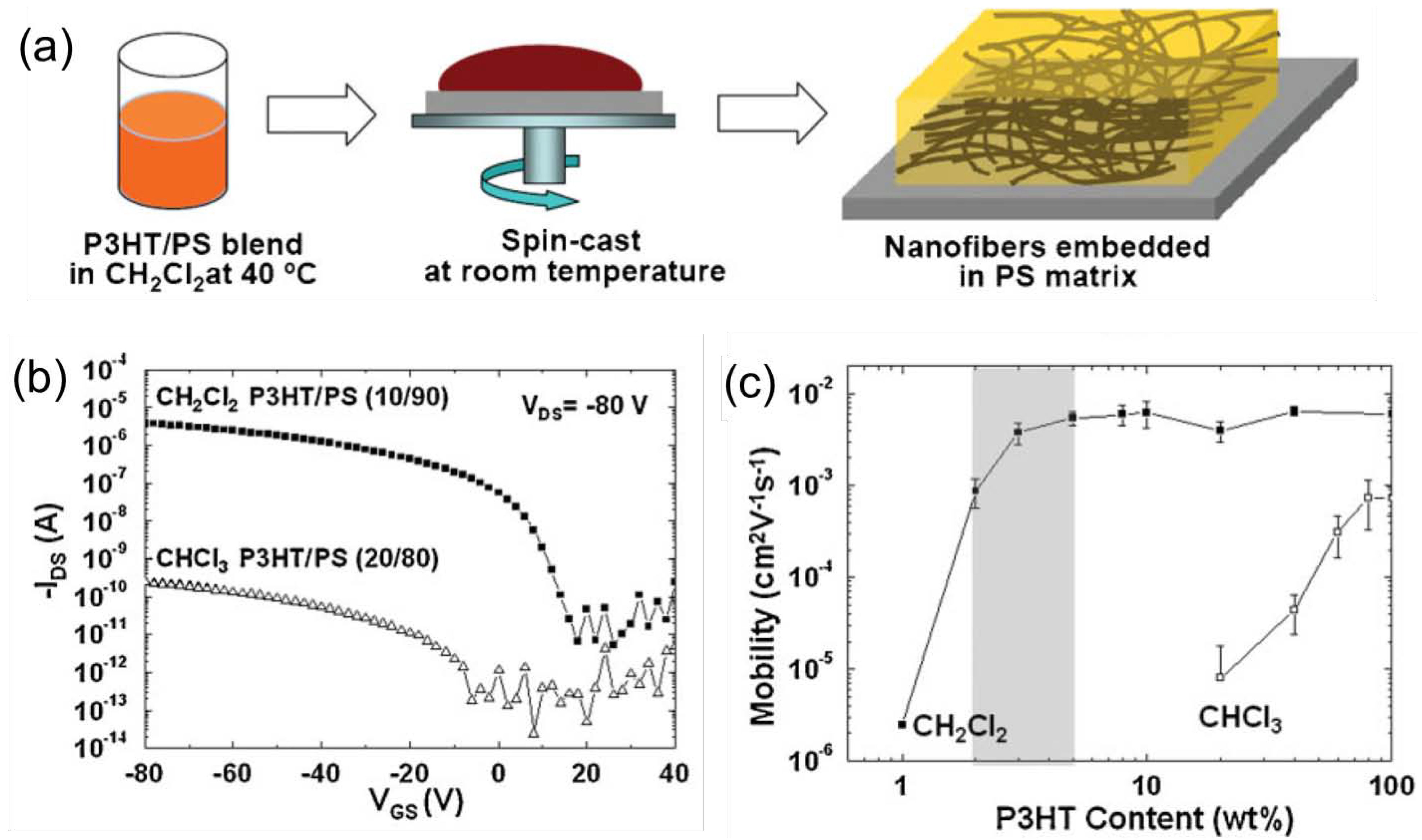
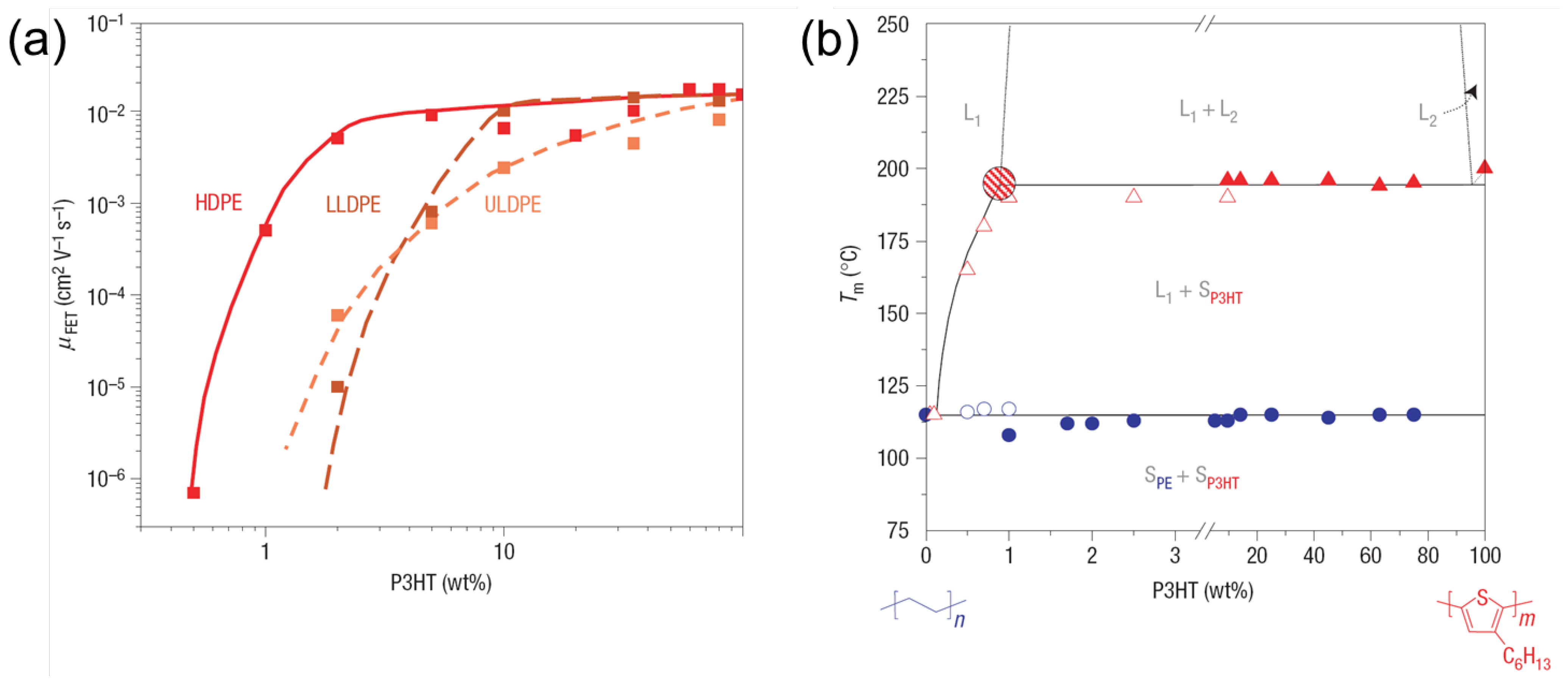
3.3. Embedded Semiconductor Nanowires

Although vertically phase-separated blended films have been successfully fabricated using semiconducting/insulating polymer blends, lateral phase separated structures and complex structures consisting of vertical and lateral structures are commonly observed [24,51]. Vertically phase-separated structures can be obtained with well-controlled polymer pairs and processing conditions (i.e., solvent evaporation rate and substrate wettability). Thus, other ways to reduce semiconductor content by blending an insulator polymer are necessary while electrical properties of OFETs based on blended films are comparable or even higher than those of OFETs based on sole-semiconductor films. Qiu et al., studied phase-separation behaviors of P3HT:polystyrene (PS) blends under a change in solubility of P3HT [52]. Figure 8a shows the schematic procedure for fabricating P3HT nanowires embedded in a PS matrix using solubility control. A P3HT:PS blended solution was prepared in CH2Cl2 at 40 °C and subsequently spin-cast on the substrate (at room temperature). Because P3HT exhibits limited solubility in CH2Cl2, the P3HT in blended solution solidified and self-assembled into nanowires on the substrate. The PS in the liquid state is then solidified by producing P3HT nanowires embedded in the PS matrix. This structure is extremely efficient for maintaining percolation of the channel at low P3HT content [52,53,54,55,56]. In addition, environmental stability of OFETs was enhanced greatly, as the PS matrix protects H2O and O2 molecules from ambient air.
Figure 8. (a) Schematic procedures for fabricating P3HT nanofibers embedded in a polystyrene (PS) matrix. P3HT:PS blend solution in CH2Cl2 was prepared at 40 °C and subsequently spin-cast on the substrate (at room temperature); (b) Electrical properties of organic field-effect transistors (OFETs) based on P3HT:PS blended films prepared with two different solvents (CH2Cl2 and CHCl3); (c) Field-effect mobilities of the OFETs as a function of P3HT content. Reproduced from [42]. Copyright 2009 Wiley.
Polymers 06 01057 g008
Figure 8b shows the electrical properties of OFETs based on P3HT:PS blended films prepared with two different solvents (CH2Cl2 and CHCl3). Because P3HT should solidify first, the structure of the embedded nanowires was not obtained in the P3HT:PS blended film from CHCl3 (good solvent for P3HT). Accordingly, OFETs based on P3HT:PS blended films from CH2Cl2 exhibit much higher field-effect mobilities than OFETs based P3HT:PS blended films from CHCl3. This is due to the unique structure of blended films (CH2Cl2), as shown in Figure 8a. In particular, this structure is extremely beneficial to reduce semiconductor content down to 3 wt%, as shown in Figure 8c. In another study, solubility control of P3HT was finely tuned by using a mixed solvent, the structure of the embedded nanowires was successfully fabricated, and semiconductor content was reduced to 1 wt% without compromising field-effect mobility [54]. In addition, this structure was also efficient as an active layer in OFETs when inkjet printing was used as the processing method [57]. The high field-effect mobility in an organic semiconductor/insulator polymer blend is an interesting research point. Lu et al., found that the performances of such blends increase dramatically upon exposure to ambient air [58]. They concluded that the high field-effect mobility obtained could be attributed to moderate doping of semiconductor nanowires in the insulator matrix.

4. Conclusions

We reviewed recent results with regard to organic semiconductor/insulator polymer blends for high-performance OFETs. The current pathway in the active layer was guaranteed by inducing vertical phase-separation, whereas a phase-separated insulator polymer could be used as a gate-dielectric or passivation layer. In contrast, an insulator polymer played a role as a processing additive for small molecular organic semiconductors. Embedded semiconductor nanowires are quite attractive for reducing semiconductor content and enhancing environmental stability, except for vertical phase-separation. Because phase separation is a complicated process that depends on molecular and processing parameters, appropriate selection of materials and processing conditions is essential for achieving high performance of organic semiconductor/insulator polymer blends.

Acknowledgments

This work was supported by the faculty research fund of Konkuk University in 2012.

Conflicts of Interest

The authors declare no conflict of interest.

References

  1. Sirringhaus, H. Reliability of organic field-effect transistors. Adv. Mater. 2009, 21, 3859–3873. [Google Scholar] [CrossRef]
  2. Braga, D.; Horowitz, G. High-performance organic field-effect transistors. Adv. Mater. 2009, 21, 1473–1486. [Google Scholar] [CrossRef]
  3. Kang, B.; Lee, W.H.; Cho, K. Recent advances in organic transistor printing processes. ACS Appl. Mater. Interfaces 2013, 5, 2302–2315. [Google Scholar] [CrossRef]
  4. Smith, J.; Hamilton, R.; McCulloch, I.; Stingelin-Stutzmann, N.; Heeney, M.; Bradley, D.D.C.; Anthopoulos, T.D. Solution-processed organic transistors based on semiconducting blends. J. Mater. Chem. 2010, 20, 2562–2574. [Google Scholar] [CrossRef]
  5. Lee, W.H.; Cho, J.H.; Cho, K. Control of mesoscale and nanoscale ordering of organic semiconductors at the gate dielectric/semiconductor interface for organic transistors. J. Mater. Chem. 2010, 20, 2549–2561. [Google Scholar] [CrossRef]
  6. Allard, S.; Forster, M.; Souharce, B.; Thiem, H.; Scherf, U. Organic semiconductors for solution-processable field-effect transistors (ofets). Angew. Chem. Int. Ed. 2008, 47, 4070–4098. [Google Scholar] [CrossRef]
  7. Podzorov, V. Organic single crystals: Addressing the fundamentals of organic electronics. MRS Bull. 2013, 38, 15–27. [Google Scholar] [CrossRef]
  8. Nielsen, C.B.; Turbiez, M.; McCulloch, I. Recent advances in the development of semiconducting dpp-containing polymers for transistor applications. Adv. Mater. 2013, 25, 1859–1880. [Google Scholar] [CrossRef]
  9. Noh, Y.Y.; Zhao, N.; Caironi, M.; Sirringhaus, H. Downscaling of self-aligned, all-printed polymer thin-film transistors. Nat. Nanotechnol. 2007, 2, 784–789. [Google Scholar] [CrossRef]
  10. Yan, H.; Chen, Z.H.; Zheng, Y.; Newman, C.; Quinn, J.R.; Dotz, F.; Kastler, M.; Facchetti, A. A high-mobility electron-transporting polymer for printed transistors. Nature 2009, 457, 679–686. [Google Scholar] [CrossRef]
  11. Klauk, H. Organic thin-film transistors. Chem. Soc. Rev. 2010, 39, 2643–2666. [Google Scholar] [CrossRef]
  12. Gelinck, G.; Heremans, P.; Nomoto, K.; Anthopoulos, T.D. Organic transistors in optical displays and microelectronic applications. Adv. Mater. 2010, 22, 3778–3798. [Google Scholar]
  13. Hambsch, M.; Reuter, K.; Stanel, M.; Schmidt, G.; Kempa, H.; Fugmann, U.; Hahn, U.; Hubler, A.C. Uniformity of fully gravure printed organic field-effect transistors. Mater. Sci. Eng. B 2010, 170, 93–98. [Google Scholar] [CrossRef]
  14. Sheats, J.R. Manufacturing and commercialization issues in organic electronics. J. Mater. Res. 2004, 19, 1974–1989. [Google Scholar]
  15. Kang, I.; Yun, H.J.; Chung, D.S.; Kwon, S.K.; Kim, Y.H. Record high hole mobility in polymer semiconductors via side-chain engineering. J. Am. Chem. Soc. 2013, 135, 14896–14899. [Google Scholar]
  16. Li, J.; Zhao, Y.; Tan, H.S.; Guo, Y.L.; Di, C.A.; Yu, G.; Liu, Y.Q.; Lin, M.; Lim, S.H.; Zhou, Y.H.; et al. A stable solution-processed polymer semiconductor with record high-mobility for printed transistors. Sci. Rep. 2012, 2, 754:1–754:9. [Google Scholar]
  17. Anthopoulos, T.D.; Tanase, C.; Setayesh, S.; Meijer, E.J.; Hummelen, J.C.; Blom, P.W.M.; de Leeuw, D.M. Ambipolar organic field-effect transistors based on a solution-processed methanofullerene. Adv. Mater. 2004, 16, 2174–2179. [Google Scholar] [CrossRef]
  18. Meijer, E.J.; de Leeuw, D.M.; Setayesh, S.; van Veenendaal, E.; Huisman, B.H.; Blom, P.W.M.; Hummelen, J.C.; Scherf, U.; Kadam, J.; Klapwijk, T.M. Solution-processed ambipolar organic field-effect transistors and inverters. Nat. Mater. 2003, 2, 834–834. [Google Scholar] [CrossRef]
  19. You, J.B.; Dou, L.T.; Hong, Z.R.; Li, G.; Yang, Y. Recent trends in polymer tandem solar cells research. Prog. Polym. Sci. 2013, 38, 1909–1928. [Google Scholar] [CrossRef]
  20. Nelson, J. Polymer: Fullerene bulk heterojunction solar cells. Mater. Today 2011, 14, 462–470. [Google Scholar] [CrossRef]
  21. Arias, A.C. Vertically segregated polymer blends: Their use in organic electronics. Polym. Rev. 2006, 46, 103–125. [Google Scholar]
  22. Moons, E. Conjugated polymer blends: Linking film morphology to performance of light emitting diodes and photodiodes. J. Phys. Condens. Mat. 2002, 14, 12235–12260. [Google Scholar] [CrossRef]
  23. Chua, L.L.; Ho, P.K.H.; Sirringhaus, H.; Friend, R.H. Observation of field-effect transistor behavior at self-organized interfaces. Adv. Mater. 2004, 16, 1609–1615. [Google Scholar] [CrossRef]
  24. Heriot, S.Y.; Jones, R.A.L. An interfacial instability in a transient wetting layer leads to lateral phase separation in thin spin-cast polymer-blend films. Nat. Mater. 2005, 4, 782–786. [Google Scholar] [CrossRef]
  25. Salleo, A. Charge transport in polymeric transistors. Mater. Today 2007, 10, 38–45. [Google Scholar] [CrossRef]
  26. Park, Y.D.; Lim, J.A.; Lee, H.S.; Cho, K. Interface engineering in organic transistors. Mater. Today 2007, 10, 46–54. [Google Scholar] [CrossRef]
  27. Chung, D.S.; Lee, D.H.; Park, J.W.; Jang, J.; Nam, S.; Kim, Y.H.; Kwon, S.K.; Park, C.E. Phase-separated polydimethylsiloxane as a dielectric surface treatment layer for organic field effect transistors. Org. Electron. 2009, 10, 1041–1047. [Google Scholar] [CrossRef]
  28. Arias, A.C.; Endicott, F.; Street, R.A. Surface-induced self-encapsulation of polymer thin-film transistors. Adv. Mater. 2006, 18, 2900–2904. [Google Scholar] [CrossRef]
  29. Qiu, L.; Lim, J.A.; Wang, X.; Lee, W.H.; Hwang, M.; Cho, K. Versatile use of vertical-phase-separation-induced bilayer structures in organic thin-film transistors. Adv. Mater. 2008, 20, 1141–1145. [Google Scholar] [CrossRef]
  30. Wang, X.H.; Lee, W.H.; Zhang, G.B.; Wang, X.H.; Kang, B.; Lu, H.B.; Qiu, L.Z.; Cho, K. Self-stratified semiconductor/dielectric polymer blends: Vertical phase separation for facile fabrication of organic transistors. J. Mater. Chem. C 2013, 1, 3989–3998. [Google Scholar] [CrossRef]
  31. Lim, J.A.; Lee, H.S.; Lee, W.H.; Cho, K. Control of the morphology and structural development of solution-processed functionalized acenes for high-performance organic transistors. Adv. Funct. Mater. 2009, 19, 1515–1525. [Google Scholar] [CrossRef]
  32. Payne, M.M.; Parkin, S.R.; Anthony, J.E.; Kuo, C.C.; Jackson, T.N. Organic field-effect transistors from solution-deposited functionalized acenes with mobilities as high as 1 cm2/V·s. J. Am. Chem. Soc. 2005, 127, 4986–4987. [Google Scholar] [CrossRef]
  33. Llorente, G.R.; Dufourg-Madec, M.B.; Crouch, D.J.; Pritchard, R.G.; Ogier, S.; Yeates, S.G. High performance, acene-based organic thin film transistors. Chem. Commun. 2009, 3059–3061. [Google Scholar]
  34. Park, S.K.; Jackson, T.N.; Anthony, J.E.; Mourey, D.A. High mobility solution processed 6,13-bis(triisopropyl-silylethynyl) pentacene organic thin film transistors. Appl. Phys. Lett. 2007, 91, 063514:1–063514:3. [Google Scholar]
  35. He, Z.R.; Li, D.W.; Hensley, D.K.; Rondinone, A.J.; Chen, J.H. Switching phase separation mode by varying the hydrophobicity of polymer additives in solution-processed semiconducting small-molecule/polymer blends. Appl. Phys. Lett. 2013, 103, 113301:1–113301:5. [Google Scholar]
  36. Park, B.; Jeon, H.G.; Choi, J.; Kim, Y.K.; Lim, J.; Jung, J.; Cho, S.Y.; Lee, C. High-performance organic thin-film transistors with polymer-blended small-molecular semiconductor films, fabricated using a pre-metered coating process. J. Mater. Chem. 2012, 22, 5641–5646. [Google Scholar] [CrossRef]
  37. Lee, W.H.; Lim, J.A.; Kwak, D.; Cho, J.H.; Lee, H.S.; Choi, H.H.; Cho, K. Semiconductor-dielectric blends: A facile all solution route to flexible all-organic transistors. Adv. Mater. 2009, 21, 4243–4248. [Google Scholar] [CrossRef]
  38. Dickey, K.C.; Anthony, J.E.; Loo, Y.L. Improving organic thin-film transistor performance through solvent-vapor annealing of solution-processable triethylsilylethynyl anthradithiophene. Adv. Mater. 2006, 18, 1721–1726. [Google Scholar] [CrossRef]
  39. Lee, W.H.; Lim, J.A.; Kim, D.H.; Cho, J.H.; Jang, Y.; Kim, Y.H.; Han, J.I.; Cho, K. Room-temperature self-organizing characteristics of soluble acene field-effect transistors. Adv. Funct. Mater. 2008, 18, 560–565. [Google Scholar] [CrossRef]
  40. Lee, W.H.; Kim, D.H.; Cho, J.H.; Jang, Y.; Lim, J.A.; Kwak, D.; Choa, K. Change of molecular ordering in soluble acenes via solvent annealing and its effect on field-effect mobility. Appl. Phys. Lett. 2007, 91, 092105:1–092105:3. [Google Scholar]
  41. Lee, W.H.; Kwak, D.; Anthony, J.E.; Lee, H.S.; Choi, H.H.; Kim, D.H.; Lee, S.G.; Cho, K. The influence of the solvent evaporation rate on the phase separation and electrical performances of soluble acene-polymer blend semiconductors. Adv. Funct. Mater. 2012, 22, 267–281. [Google Scholar] [CrossRef]
  42. Subramanian, S.; Park, S.K.; Parkin, S.R.; Podzorov, V.; Jackson, T.N.; Anthony, J.E. Chromophore fluorination enhances crystallization and stability of soluble anthradithiophene semiconductors. J. Am. Chem. Soc. 2008, 130, 2706–2708. [Google Scholar]
  43. Goffri, S.; Muller, C.; Stingelin-Stutzmann, N.; Breiby, D.W.; Radano, C.P.; Andreasen, J.W.; Thompson, R.; Janssen, R.A.J.; Nielsen, M.M.; Smith, P.; et al. Multicomponent semiconducting polymer systems with low crystallization-induced percolation threshold. Nat. Mater. 2006, 5, 950–956. [Google Scholar] [CrossRef]
  44. Kjellander, B.K.C.; Smaal, W.T.T.; Anthony, J.E.; Gelinck, G.H. Inkjet printing of tips-pen on soluble polymer insulating films: A route to high-performance thin-film transistors. Adv. Mater. 2010, 22, 4612–4616. [Google Scholar] [CrossRef]
  45. Madec, M.B.; Crouch, D.; Llorente, G.R.; Whittle, T.J.; Geoghegan, M.; Yeates, S.G. Organic field effect transistors from ambient solution processed low molar mass semiconductor-insulator blends. J. Mater. Chem. 2008, 18, 3230–3236. [Google Scholar]
  46. Madec, M.B.; Smith, P.J.; Malandraki, A.; Wang, N.; Korvink, J.G.; Yeates, S.G. Enhanced reproducibility of inkjet printed organic thin film transistors based on solution processable polymer-small molecule blends. J. Mater. Chem. 2010, 20, 9155–9160. [Google Scholar] [CrossRef]
  47. Kang, J.; Shin, N.; Jang, D.Y.; Prabhu, V.M.; Yoon, D.Y. Structure and properties of small molecule-polymer blend semiconductors for organic thin film transistors. J. Am. Chem. Soc. 2008, 130, 12273–12275. [Google Scholar] [CrossRef]
  48. Ohe, T.; Kuribayashi, M.; Yasuda, R.; Tsuboi, A.; Nomoto, K.; Satori, K.; Itabashi, M.; Kasahara, J. Solution-processed organic thin-film transistors with vertical nanophase separation. Appl. Phys. Lett. 2008, 93, 053303:1–053303:3. [Google Scholar]
  49. Shin, N.; Kang, J.; Richter, L.J.; Prabhu, V.M.; Kline, R.J.; Fischer, D.A.; DeLongchamp, D.M.; Toney, M.F.; Satija, S.K.; Gundlach, D.J.; et al. Vertically segregated structure and properties of small molecule-polymer blend semiconductors for organic thin-film transistors. Adv. Funct. Mater. 2013, 23, 366–376. [Google Scholar] [CrossRef]
  50. Kim, Y.H.; Anthony, J.E.; Park, S.K. Polymer blended small molecule organic field effect transistors with improved device-to-device uniformity and operational stability. Org. Electron. 2012, 13, 1152–1157. [Google Scholar] [CrossRef]
  51. Jo, S.B.; Lee, W.H.; Qiu, L.Z.; Cho, K. Polymer blends with semiconducting nanowires for organic electronics. J. Mater. Chem. 2012, 22, 4244–4260. [Google Scholar] [CrossRef]
  52. Qiu, L.Z.; Lee, W.H.; Wang, X.H.; Kim, J.S.; Lim, J.A.; Kwak, D.; Lee, S.; Cho, K. Organic thin-film transistors based on polythiophene nanowires embedded in insulating polymer. Adv. Mater. 2009, 21, 1349–1353. [Google Scholar] [CrossRef]
  53. Qiu, L.Z.; Xu, Q.; Lee, W.H.; Wang, X.H.; Kang, B.; Lv, G.Q.; Cho, K. Organic thin-film transistors with a photo-patternable semiconducting polymer blend. J. Mater. Chem. 2011, 21, 15637–15642. [Google Scholar] [CrossRef]
  54. Qiu, L.Z.; Wang, X.; Lee, W.H.; Lim, J.A.; Kim, J.S.; Kwak, D.; Cho, K. Organic thin-film transistors based on blends of poly(3-hexylthiophene) and polystyrene with a solubility-induced low percolation threshold. Chem. Mater. 2009, 21, 4380–4386. [Google Scholar] [CrossRef]
  55. Kim, F.S.; Jenekhe, S.A. Charge transport in poly(3-butylthiophene) nanowires and their nanocomposites with an insulating polymer. Macromolecules 2012, 45, 7514–7519. [Google Scholar] [CrossRef]
  56. Kramer, T.J.; Chew, A.R.; Schiros, T.; Kymissis, I.; Herman, I.P. Poly-(3)hexylthiophene nanowire networks for versatile fabrication of bulk heterojunctions with increased active volume. J. Vac. Sci. Technol. B 2013, 31, 031209:1–031209:8. [Google Scholar]
  57. Lim, J.A.; Kim, J.H.; Qiu, L.; Lee, W.H.; Lee, H.S.; Kwak, D.; Cho, K. Inkjet-printed single-droplet organic transistors based on semiconductor nanowires embedded in insulating polymers. Adv. Funct. Mater. 2010, 20, 3292–3297. [Google Scholar] [CrossRef]
  58. Lu, G.H.; Blakesley, J.; Himmelberger, S.; Pingel, P.; Frisch, J.; Lieberwirth, I.; Salzmann, I.; Oehzelt, M.; di Pietro, R.; Salleo, A.; et al. Moderate doping leads to high performance of semiconductor/insulator polymer blend transistors. Nat. Commun. 2013, 4, 1588:1–1588:8. [Google Scholar]

