Modeling, Analysis, and Realization of Permanent Magnet Synchronous Motor Current Vector Control by MATLAB/Simulink and FPGA

Department of Electrical Engineering, National Chin-Yi University of Technology, Taichung 41170, Taiwan
*
Author to whom correspondence should be addressed.
Machines 2017, 5(4), 26; https://doi.org/10.3390/machines5040026
Submission received: 13 September 2017
/
Revised: 8 October 2017
/
Accepted: 8 October 2017
/
Published: 28 October 2017
(This article belongs to the Special Issue High Speed Motors and Drives: Design, Challenges and Applications)
Abstract
:In this paper, we present the modeling, analysis, and realization of current vector control for a permanent magnet synchronous motor (PMSM) drive using MATLAB/Simulink and a field programmable gate array (FPGA). In AC motor drive systems, most of the current vector controls are realized by digital signal processors (DSPs) because of their complete and compact hardware functions. However, the performances of drive systems realized by low-cost DSP are limited by the hardware structure and computation capacity, which may lead to the difficulty of reaching a fast enough response, above all, for those motors with a small electrical time constant. Therefore, we use FPGA to speed up the calculation about the current vector control to attain a fast response. Simulations and practical experimental results are used to verify the correctness and performance of the designed full hardware system.
1. Introduction
The rapid development of high-performance and low-cost digital signal processors (DSP) has encouraged researchers to design motor drives with DSP. The functionality of a DSP is dependent on the demands for the particular requirements and processing speed. Since motor control using DSP has been widely developed by researchers and industry, IC manufacturers have, thus, designed and produced specific DSPs for motor control, such as the TI TMS320F28 series DSP, Microchip dsPIC, etc. Those motor control schemes with DSPs as the controllers have advantages, such as simple circuitry, software control, and flexibility in adaptation to various motor control requirements and applications. However, it is important to have an inner current control loop with a short time constant in order to obtain a rapid dynamic response on velocity or position control. To this requirement stated above, the calculation time to decide the desired switching pattern with the space vector pulse width modulation (SVPWM) strategy is requested as short as possible. Under this consideration, the inherent properties of DSP with sequential processing and software execution may make the system hardly reach the desired performance on the current loop control with high sampling frequency, e.g., 40 kHz or above, especially for a fixed-point DSP, or the developed algorithm without support by the build-in hardware of DSP. Therefore, a DSP with a floating point processor and high frequency clock is developed and used; however, this carries a high price.
Current feedback can be accomplished by Hall sensors or resistors, and sometimes the analog sinusoidal signal is processed by a low pass filter to remove the components, including those from modulation. However, phase lag and amplitude attenuation of the winding current from the Hall sensor and the low pass filter should be taken into consideration when the system is operated at high sampling frequency, which is closed to the bandwidth of Hall current sensor or low pass filter.
MATLAB/Simulink, produced by the MathWorks, Inc., is often used to the analysis and simulation for control purpose, and the controller design of modern power electronics and motor drive systems by field programmable gate arrays (FPGAs) has become more and more important. Thus, MATLAB/Simulink has been used as an alternative method to automatically generate a readable and portable IEEE standards compliant hardware description language (HDL) to realize the desired system which is generally and formerly built by DSP [1]. System design with MATLAB/Simulink makes complicated design easier. The designers can easily build and simulate their hardware control system by solving the conventional control problem with MATLAB/Simulink. Of course, some, or even many, modifications are needed to realize the developed hardware systems on a selective FPGA. However, for researchers, the hardware circuit design starting from MATLAB/Simulink is another choice to shorten the developing time.
An FPGA is fully customizable, allowing a completely flexible design which is custom-made for the particular type of control technology. Furthermore, an FPGA is field programmable, and further functionalities can be added anytime and anywhere when they are necessary [2]. FPGA-based digital controllers have, thus, been implemented successfully in motor drives, such as induction motors (IMs) [3], permanent magnet synchronous motors (PMSMs) [4,5,6,7], stepping motors [8], brushless DC motors [9], and switched reluctance motors [2]. Additionally, FPGAs are also used in the implementations of controllers, such as PID controllers [10], fuzzy controllers [4,11], tracking controllers [8], and for the realization of SVPWM modules [6].
In this study, the procedure of designing an FPGA-based current vector control for a PMSM drive system is demonstrated. The requirements of the design include the fast winding current responses, the realizable intellectual property (IP) for vector control, and the complete interfaces and peripherals. At first, the system is designed via MATLAB/Simulink on the system level, simulated by ModelSim, produced by Mentor Graphics Corporation, to evaluate the correctness, and converted into the Verilog HDL code as a vector control IP. Next, some modifications are made for the developed IP systems in order to be realizable by the specific selected FPGA. To finish the design of the hardware system, the interfaces for an analog to digital converter (ADC), digital to analog converter (DAC), serial/parallel converter, quadrature encoder pulse (QEP) counter, SVPWM module, and digital filter for speed moving average and for encoder signals are included in the design. Finally, the designed overall hardware circuits are applied to the PMSM drive system to practically evaluate the performances of the FPGA-based system by showing the sinusoidal steady-state response.
This paper is organized as follows. In Section 2, the mathematical descriptions regarding the electrical circuit of PMSM motor are given. The simulated and experimental systems designed and created by MATLAB/Simulink are shown in Section 3. In Section 4, the simulated results based on the system created in Section 3, and the experimental results based on the FPGA, power module, and PMSM motor are demonstrated. Finally, the conclusions are given in Section 5.
2. The Electrical Model of Permanent Magnet Synchronous Motor
The typical mathematical model of a PMSM is described in the dq-axis synchronous rotating reference frame as follows [4]:
where and are the d- and q-axis voltages; and are the d- and q-axis currents; is the phase winding resistance; and are the d- and q-axis inductances, and ; is the rotating speed of magnet flux; and is the permanent magnet flux linkage.
Generally, the current control of PMSM is based on the vector control approach, and the generated torque, , can be represented as:
where is the pole number, and is the torque constant. (3) shows that the generated torque is proportional to the q-axis current under decoupling control.
3. Analysis and Design for PMSM Drive System Based on MATLAB/Simulink
3.1. The Block Diagram of PMSM Drive System
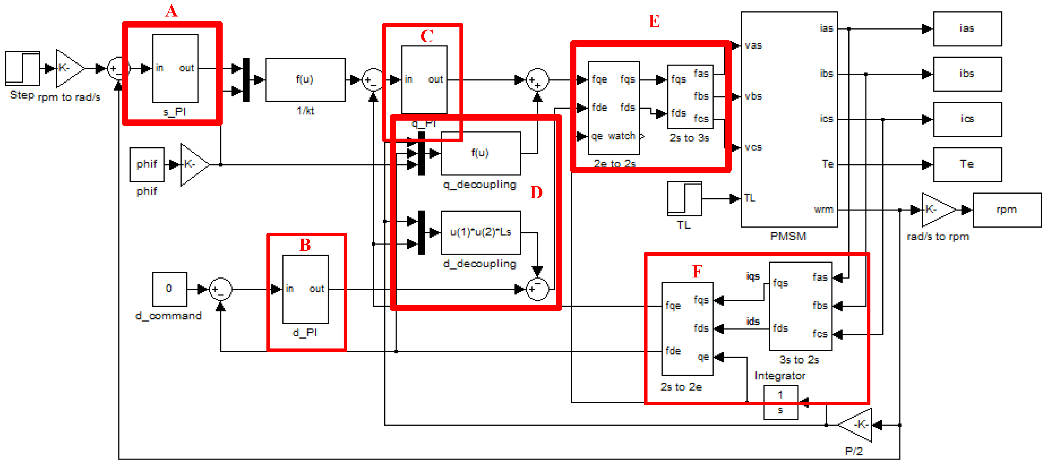
A complete velocity control model created in MATLAB/Simulink is shown in Figure 1, which includes the three PI controllers (block A for speed control, block B for d-axis current control, and block C for q-axis current control), the decoupling control (block D), the / coordinate transformation (blocks E and F), and the PMSM model. In the study, we mainly consider the current loop controller design, especially the q-axis one. The structure of the enhanced current control loop is based on a standard field-oriented control, and the two voltages, and in Equations (1) and (2), for d- and q-axis circuits are, respectively, determined from the two PI controllers (blocks B and C). Since the decoupling control is assumed, the parameters of the current loop PI controllers are designed separately.
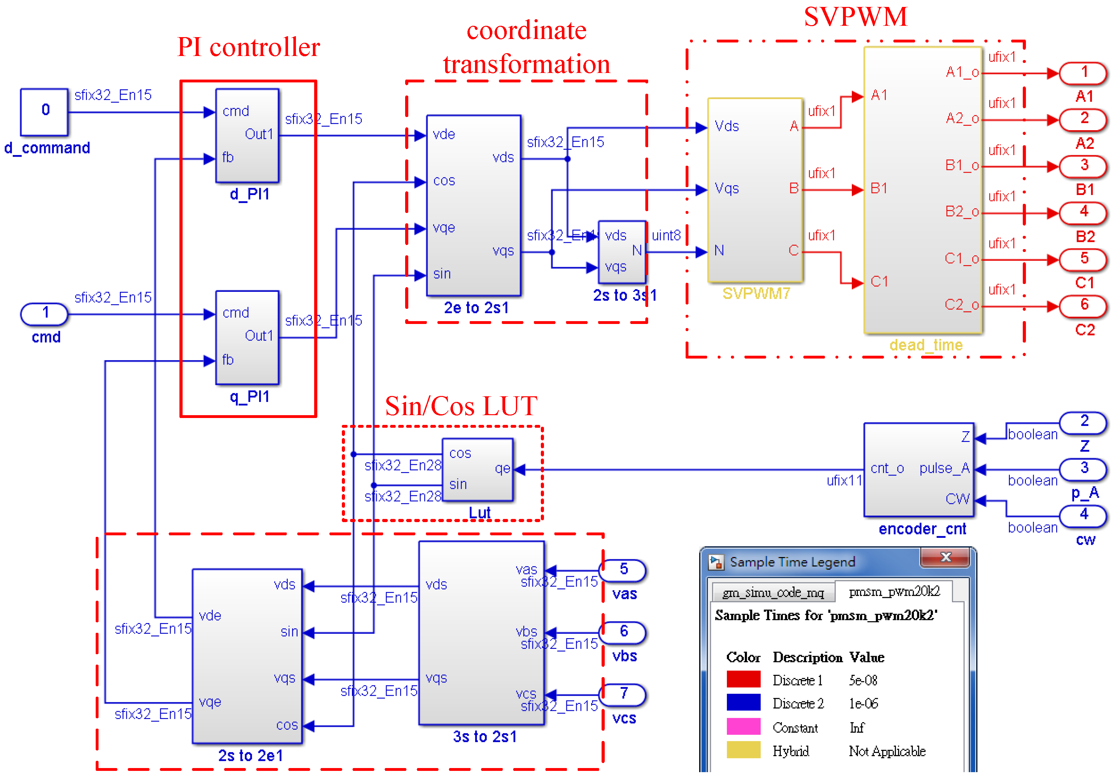
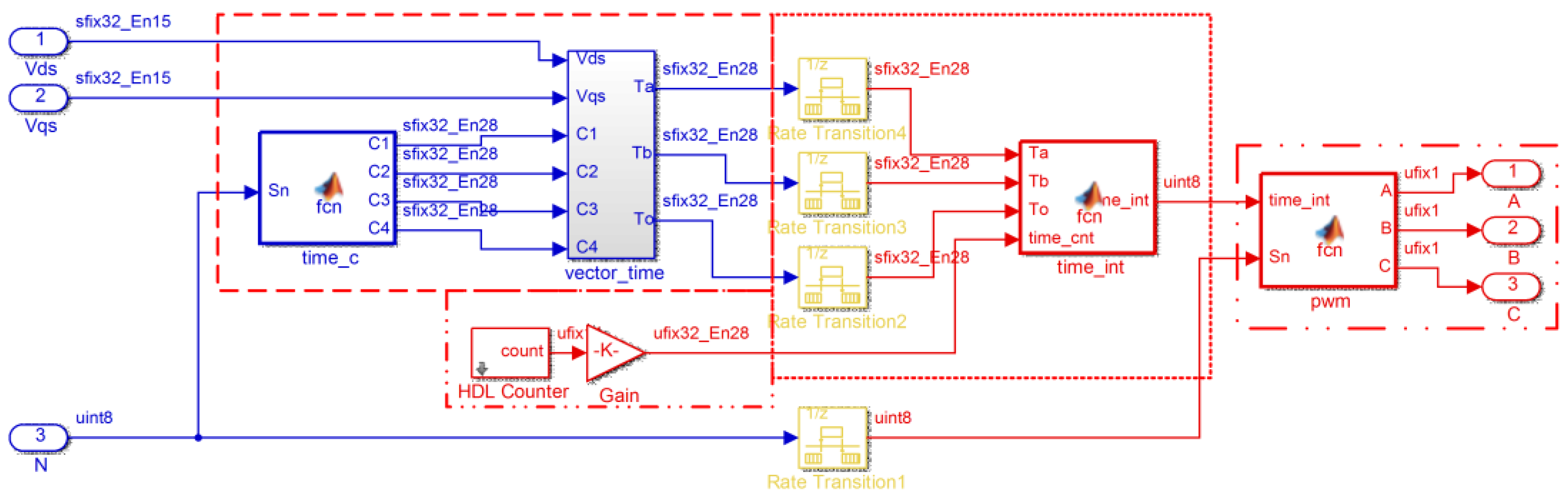
In this study, the controllers for current loop are exclusively realized by FPGA. In order to reach the goal of fast current response, all the components’ delays of the current loop are taken into consideration. The main delays are from the 12-bit ADCs, the quadrature encoder pulse (QEP) counter, and the SVPWM module, etc. The block diagram of vector control represented by Verilog HDL is shown in Figure 2, where the sin/cos look up table (LUT), the two PI controllers, the four coordinate transformation modules and the SVPWM module are included. In Figure 2, since the rotor is a permanent magnet, the d-axis command is set to zero. Additionally, the q-axis command which is proportional to the desired torque is from the PI controller of velocity control. The block named as ‘encoder_cnt’ is the QEP counter, which provides the information of the rotor position for position and velocity feedback, as well as coordinate transformation. The input signals of QEP are named as Z, P_A, and CW, which come from the encoder on the motor. In Figure 2, the blue blocks are operated at a 20 kHz clock.
3.2. The Design of Hardware PI Controller
The PI controller realized by FPGA first comes from the continuous system:
where and are the parameters of the PI controller. Equation (4) is digitalized by the backward difference method:
where is the sampling time. To substitute Equation (5) into Equation (4), the resulting digital PI controller is as follows:
In Equation (6), the I-control is with the iteration operation, and one limiter is added to the accumulator output to prevent saturation. Since the sampling frequency for current control loop is normally in the scale of 10 kHz–20 kHz, the sampling time is quite small. Thus, to consider the resolution of parameters and avoid the truncated error, the variables are represented in 32-bit numbers. The realized hardware PI controllers are shown in Figure 3 where the command (cmd) and system feedback (fb) are the inputs. The data bus is programmed as 32 bits, in which 15 bits for the integer part, 16 bits for the fractional part, and one bit for the sign bit. Additionally, in Figure 3, the process of the error signal is in parallel (the P and I actions) to enhance the performance and reduce the calculation time.
3.3. The Clarke, Park, Inverse Park, and Inverse Clarke Transformations
To implement the functions of Clarke, Park, Inverse Park, and Inverse Clarke transformations, the sin() and the cos() tables are created. Each of the elements of the tables is represented as 32-bit numbers, with three bits for the integer part, 28 bits for the fractional part, and one bit for the sign bit. The index is from the encoder counter which is also programmed as a 32-bit number.
3.4. The SVPWM Model
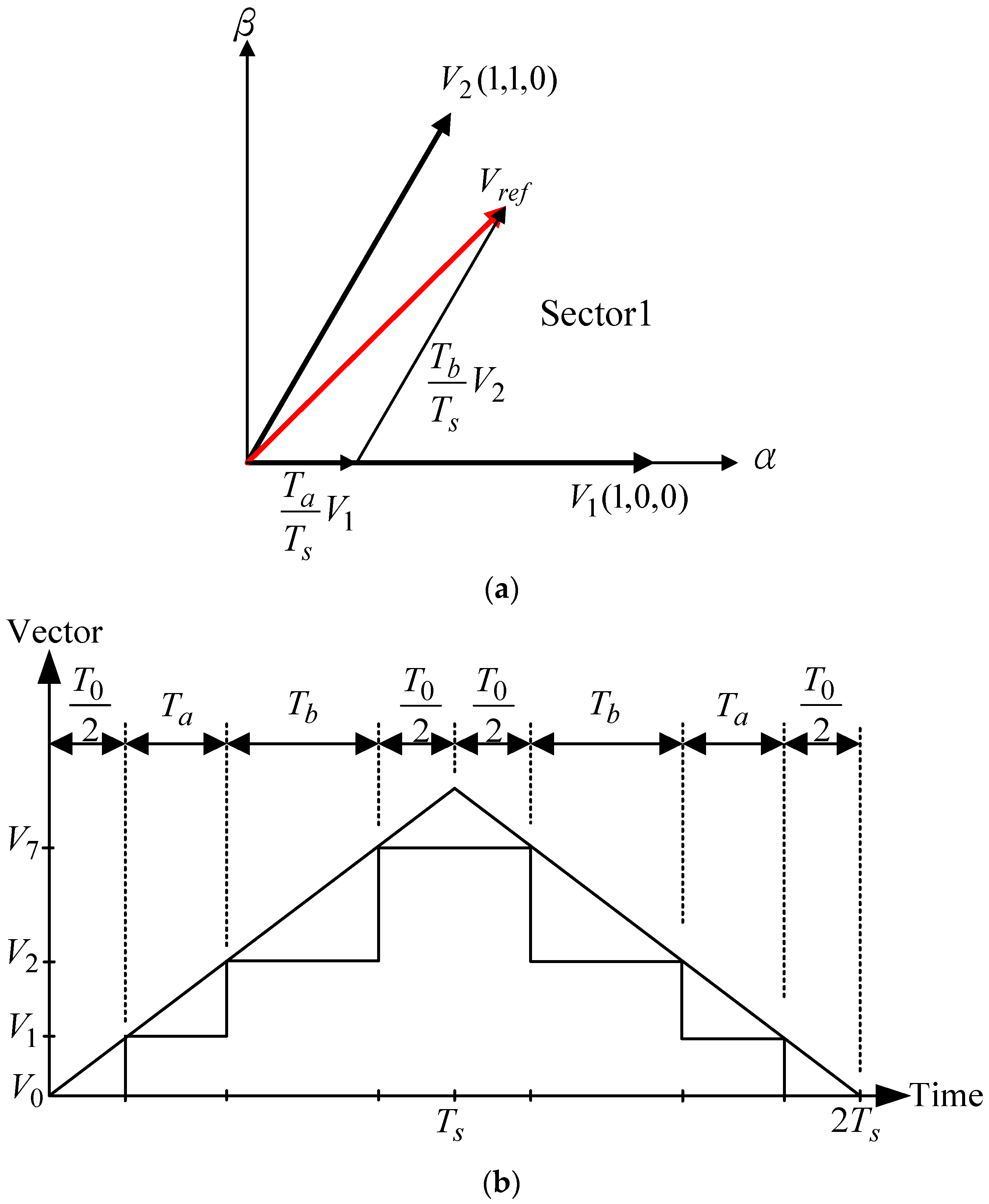
The SVPWM module is built to obtain the desired voltage by outputting six gate driver signals, A1, A2, B1, B2, C1, and C2, as shown in Figure 2, and more details are shown in Figure 4. The period of SVPWM is set as 50 with a symmetrical structure, and the dead-time is set as 1 . In Figure 4, the control voltages, and from PI controllers, are used to generate the corresponding switching pattern [6], examples are shown in Figure 5, where Figure 5a indicates that the desired vector voltage is in Sector 1, and can be synthesized by the vectors , , , and . The turn-on sequences are shown in Figure 5b, where the active vectors are and , non-effective vectors are and , and:
where is the duration for the system in zero vectors and , for vector and for vector in the condition of Figure 5b. The total active time is (), and the duty cycle for this condition is defined as:
The SVPWM system is considered as having the largest hardware delay in the block diagram of Figure 2, and the value is 50 (20 kHz sampling frequency).
We designed all the components separately, and added D-F-Fs for those blocks marked by 1 for the sake of synchronization. They are shown in Figure 6. Additionally, the ADC needs 4 to convert the analog current signals into digital values. By Figure 6, the total computation times to determine the duty cycle (Equation (8)) for the SVPWM module are 8 , which are shorter than the 50 of the SVPWM period. Thus, the total propagation time from the ADC to the entry of the SVPWM block could be omitted, i.e., the run time of 50 of the SVPWM period is sufficient to accomplish all of the calculations.
In the study, the object is to obtain a closed-loop current control system with bandwidth higher than 1 kHz, which is equivalent to having a closed-loop pole greater than 6280 rad/s. To this requirement, the electrical time constant of the motor stator winding, the choice of the current sensor, the processing of the current signal, and the execution period of SVPWM to generate the control voltages are especially taken into consideration. Among them, the SVPWM module is the greatest obstacle in the control loop due to the fact that it needs the longest time to complete a cycling operation. The design procedures are as follows.
Assuming the system is under decoupling control, the q-axis equivalent closed-loop control can be simplified as shown in Figure 7. The transfer function of q-axis circuit is simplified as:
and the closed-loop relation of Figure 7 could be represented as:
where is the q-axis current command. In (10), there are one zero at and two poles to be determined.
With the consideration to get a wide bandwidth response, a large proportional gain of is chosen, and the ratio is made:
In Equation (11), the parameters and of the PI controller are also programmed as 32-bit numbers. With the setting, we could easily obtain the desired resolution for the parameters of the controller. According to the assumption of Equation (11), Equation (10) can be simplified as:
Since the value of is greater than the value of , Equation (12) can be further rewritten as:
Regarding Equations (12) and (13), they show that the parameter can mainly be used to determine the bandwidth of the q-axis circuit. Additionally, the control parameters of the d-axis can be obtained in the same manner.
The characteristic of Equation (12) is a second-order band-pass filter, which has the lower 3 dB frequency and upper 3 dB frequency. However, since the lower 3 dB frequency is small enough to be omitted, the bandwidth of Equation (12) is very close to that of Equation (13). Due to the fact that the electrical circuit is operated at a higher frequency (the sampling frequency, ), the approximation of Equation (13) is valid.
It is noted that the hardware control system for the PMSM current vector control described in the paper may also be used for the current vector control of induction motor, except the command of the d-axis current, which will not be set to zero due to the structure of the rotor.
4. Simulation, Experiment, and Discussion
Simulation and experiment are both done to show the performance of the designed hardware control system. The characteristics of the PMSM motor are shown in Table 1. The number of poles is 10; the stator resistance and inductance are, respectively, 3.5 and 13 [12]. The electrical time constant is about 3.71 . A closed-loop control with PI controller as the kernel is used to compensate the system, and the expected closed-loop bandwidth is equal to, or greater than, 1 kHz. To reach the goals, the of the speed PI controller is first designed according to Equation (13), and chosen as for this system. The bandwidth of the equivalent current loop system is Hz. The parameters of PI controller are and , the sampling frequency is set as , which is eight times the desired system bandwidth, and this fits the criterion of digital signal processing. With the above-mentioned parameters, we have the equivalent system:
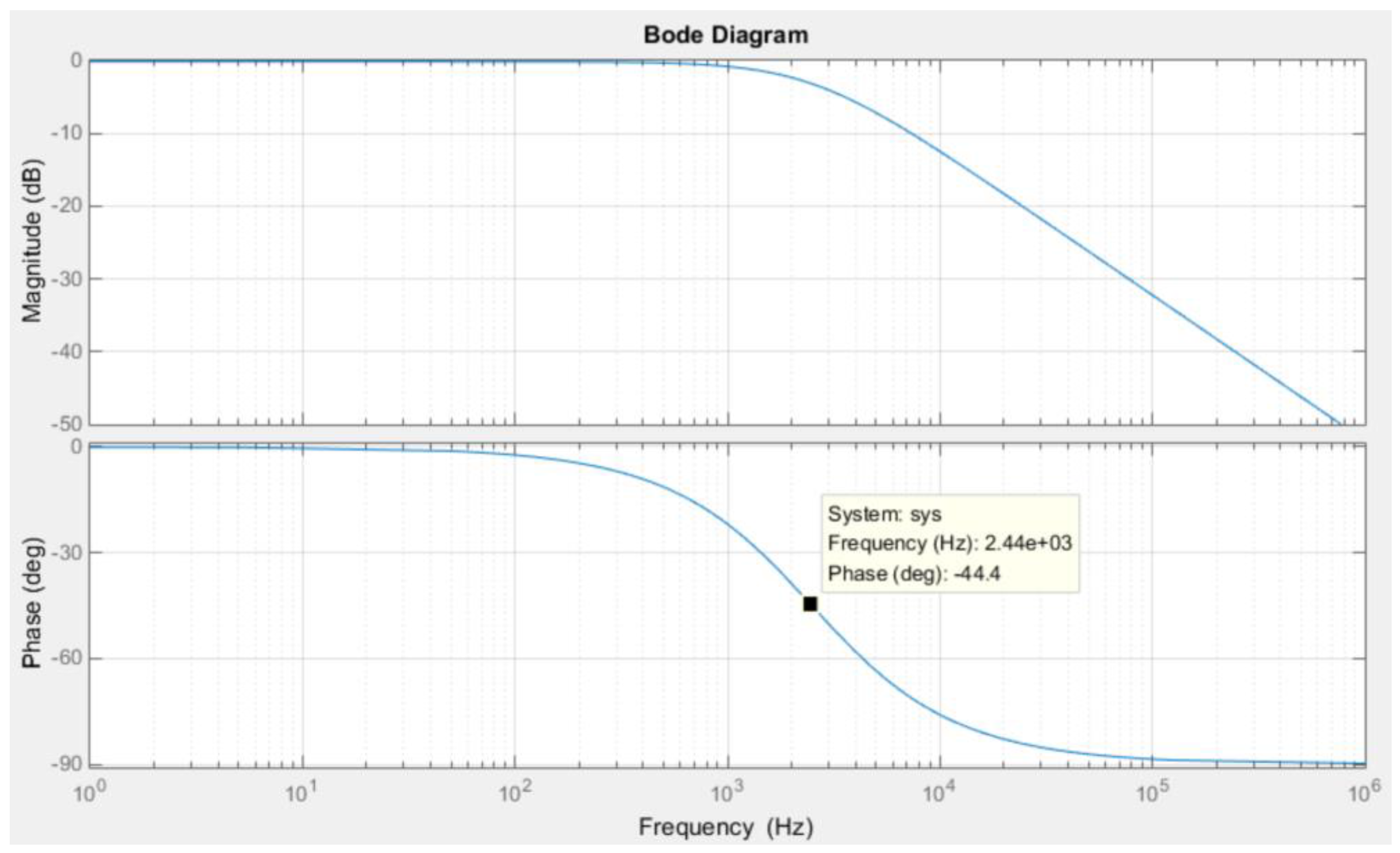
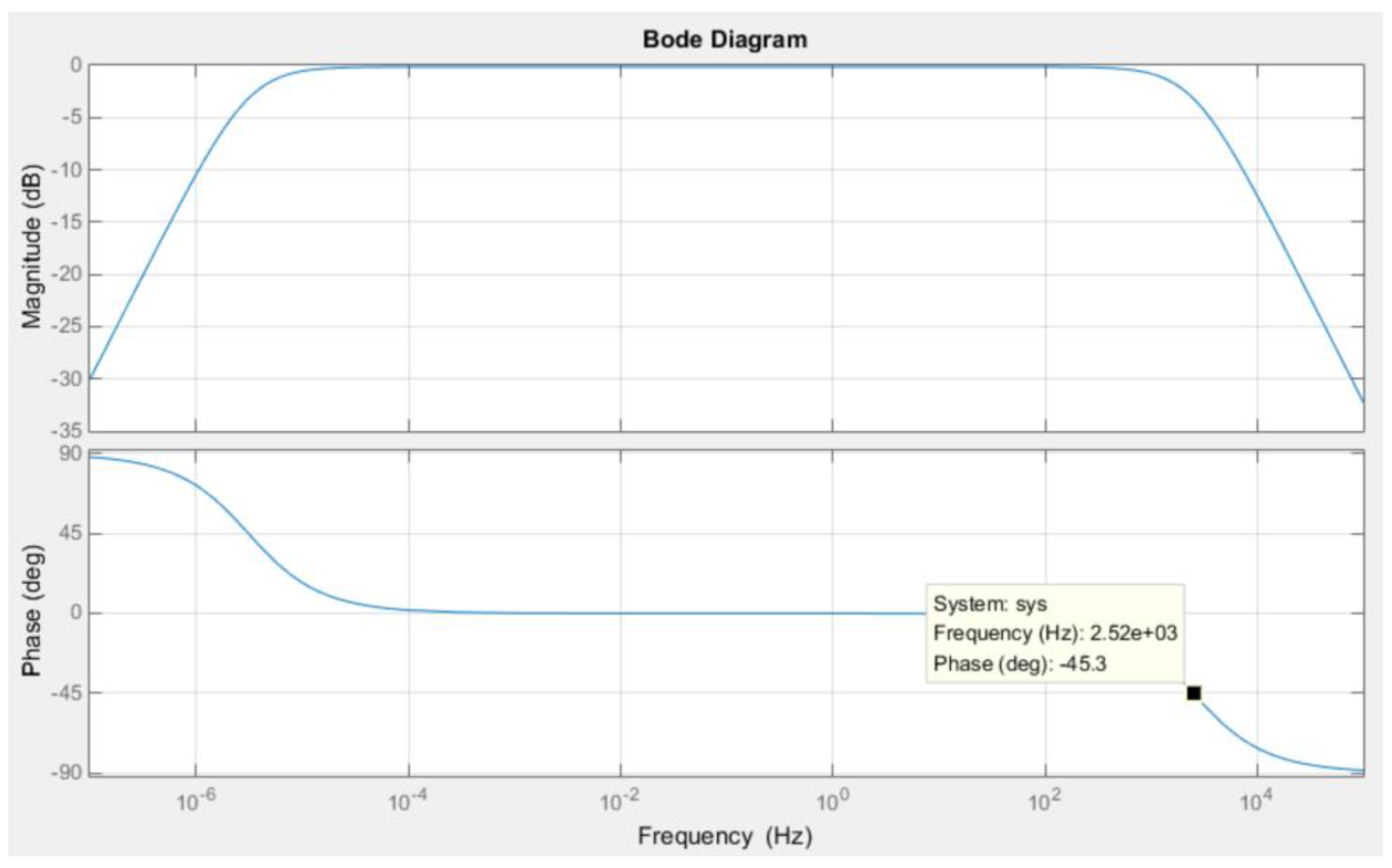
The corresponding frequency response of Equation (14) is shown in Figure 8 with MATLAB, and the bandwidth is about 2.5 kHz, which is greater than the desired 1 kHz. As stated in the last section, Equation (12) is a band-pass system, and the frequency response is shown in Figure 9. It is noted that, in the region of low frequency, the response of Figure 8 is different from the one of Figure 9. Nevertheless, the system is operated at , which is far away from the lower 3 dB frequency, which is about 5 rad/s, and the responses for both systems are very similar.
The waveform of the command is from a previously-built discrete-type sinusoidal signal, which is programmed and stored in the memory of the FPGA, and all the data are 32-bit numbers. The FPGA used to implement the system is made with an Altera Corp. model Cyclone III EP3C10E144C8. Since the main objects are focused on the inner current closed-loop control to yield a fast response with the dedicated system by SVPWM, the results regarding the current loop of the q-axis are the main components to be shown.
4.1. The Simulation Results
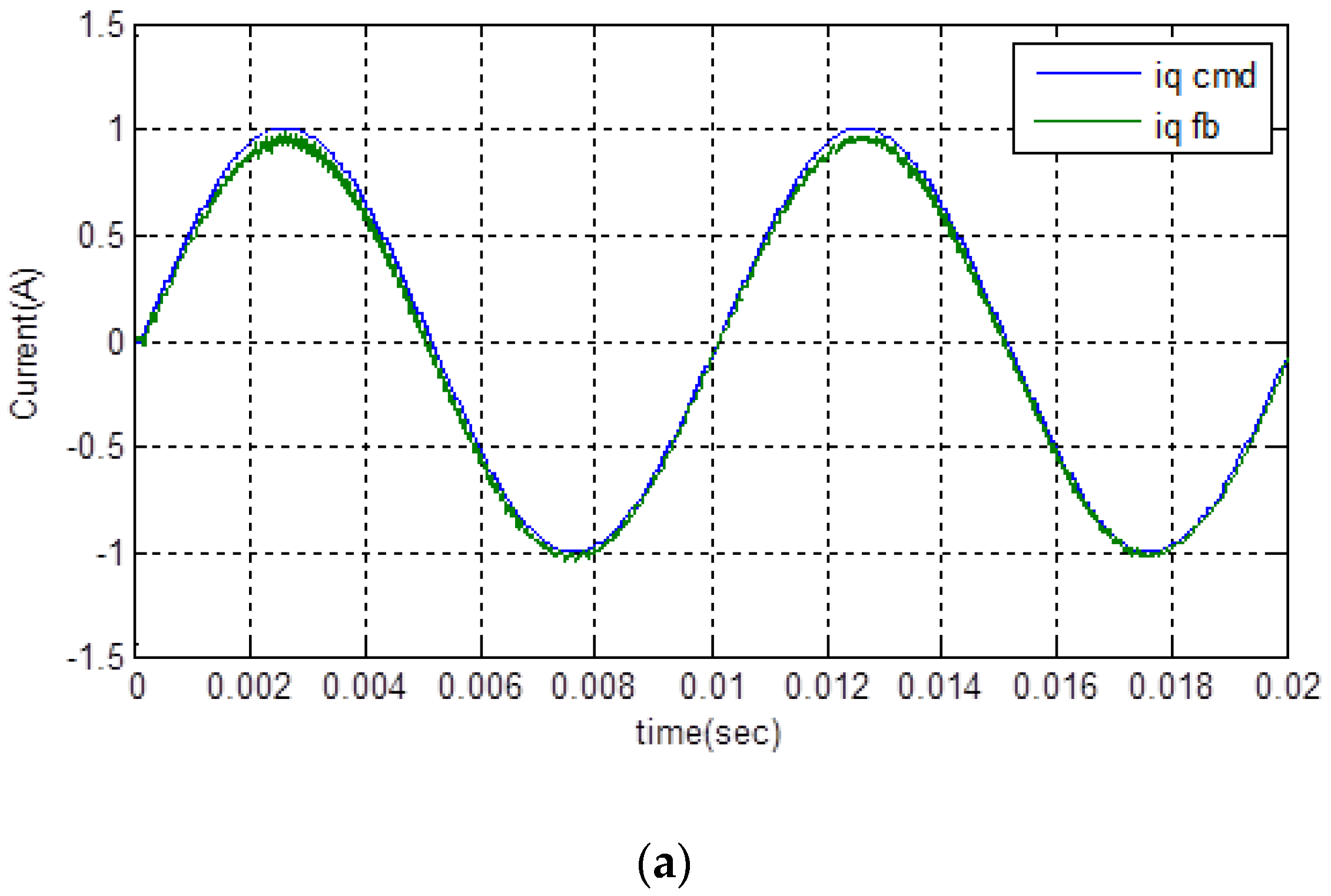
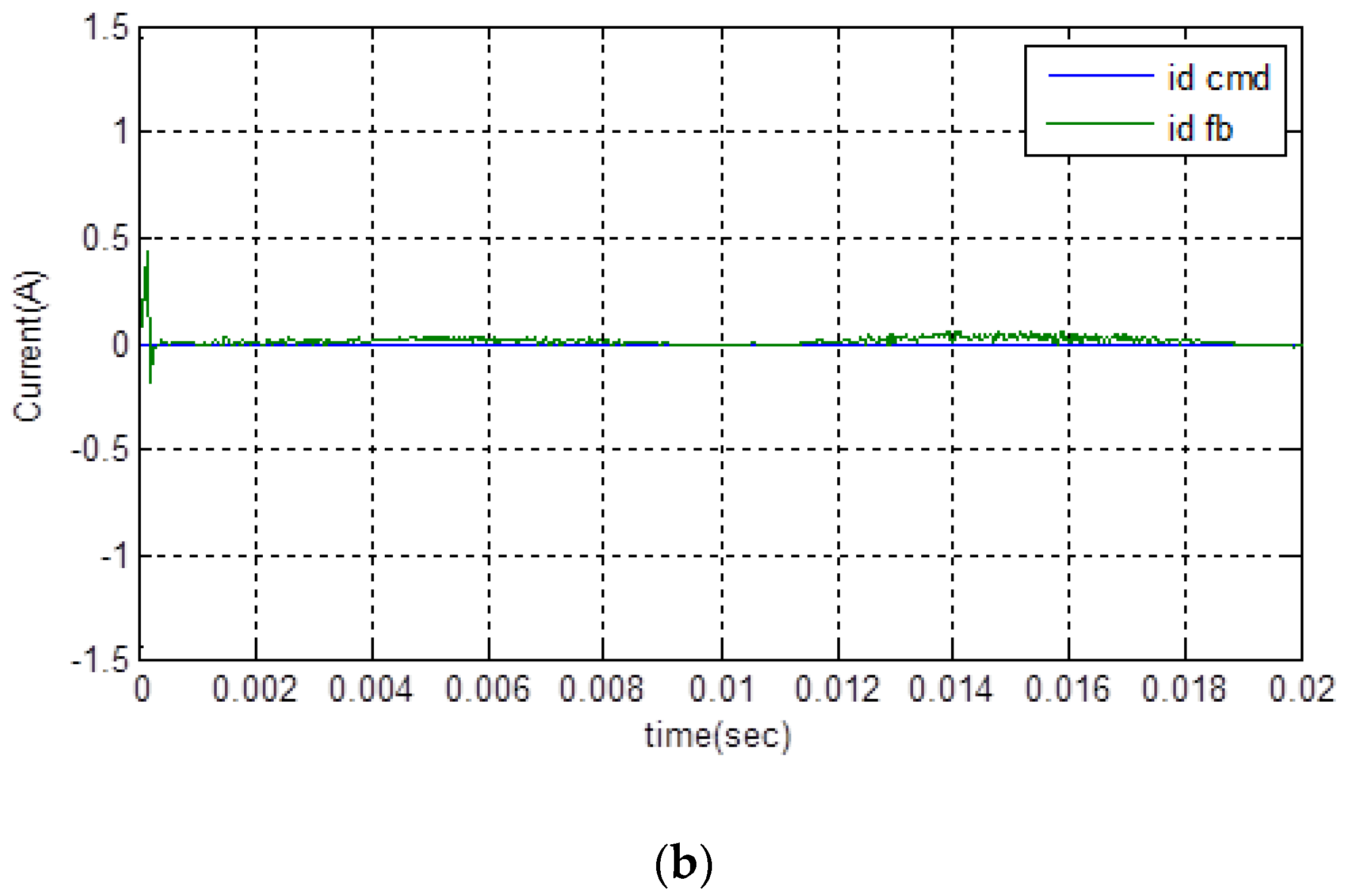
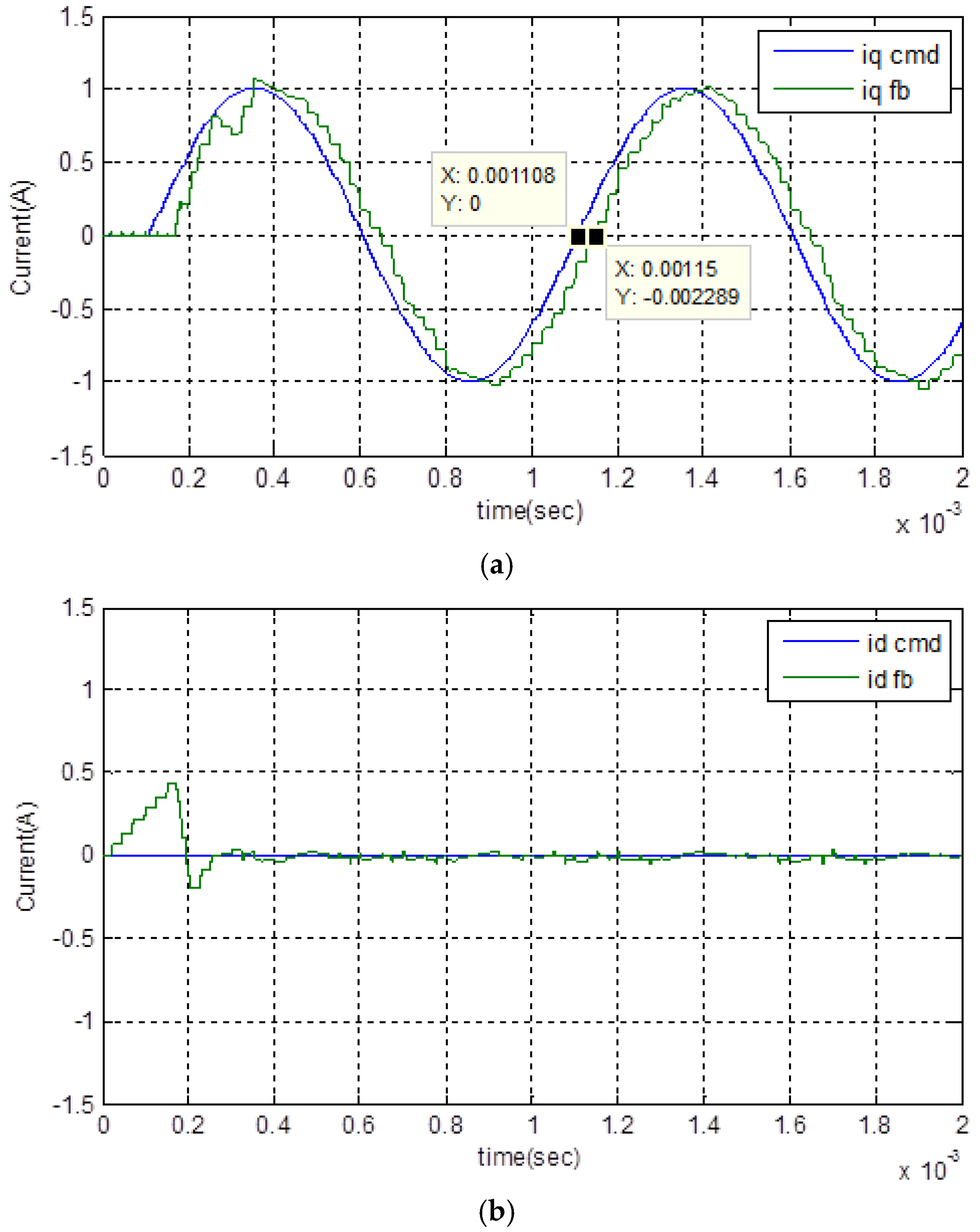
The simulation is first performed on the MATLAB/Simulink platform. Figure 10 and Figure 11 are the simulation results with the control block diagram as shown in Figure 1. To prevent saturation of the PI controller and the PMSM drive, the amplitude of current command is set to 1 A. In the following, the results for the commands at 100 Hz and 1 kHz sinusoidal input are demonstrated, respectively. Figure 10 shows the results at 100 Hz, where and are, respectively, the 100 Hz sinusoidal command inputs, and and are the current feedbacks. The responses and commands of the two figures are very close to each other. In Figure 10a, there is only a small DC offset between the two traces, and in Figure 10b, the d-axis current is very small, except for the transient duration at start. Furthermore, we set 1 kHz sinusoidal commands as the input, and the current amplitude is also approximately 1 A. Figure 11 is the simulated results. As the points marked on Figure 11a of the q-axis response, the time delay is 0.00115 – 0.001108 = 0.000042 s; it is equivalent to a phase lag . Additionally, the difference of the amplitude between and is very small. Since the phase delay is less than , and nearly no amplitude drops off, the q-axis equivalent circuit under feedback control, thus, has a bandwidth greater than 1 kHz. Figure 11b shows that the d-axis current is still small, except for the transient duration shown in the results of Figure 10b.
4.2. The Experimental Setup and Results
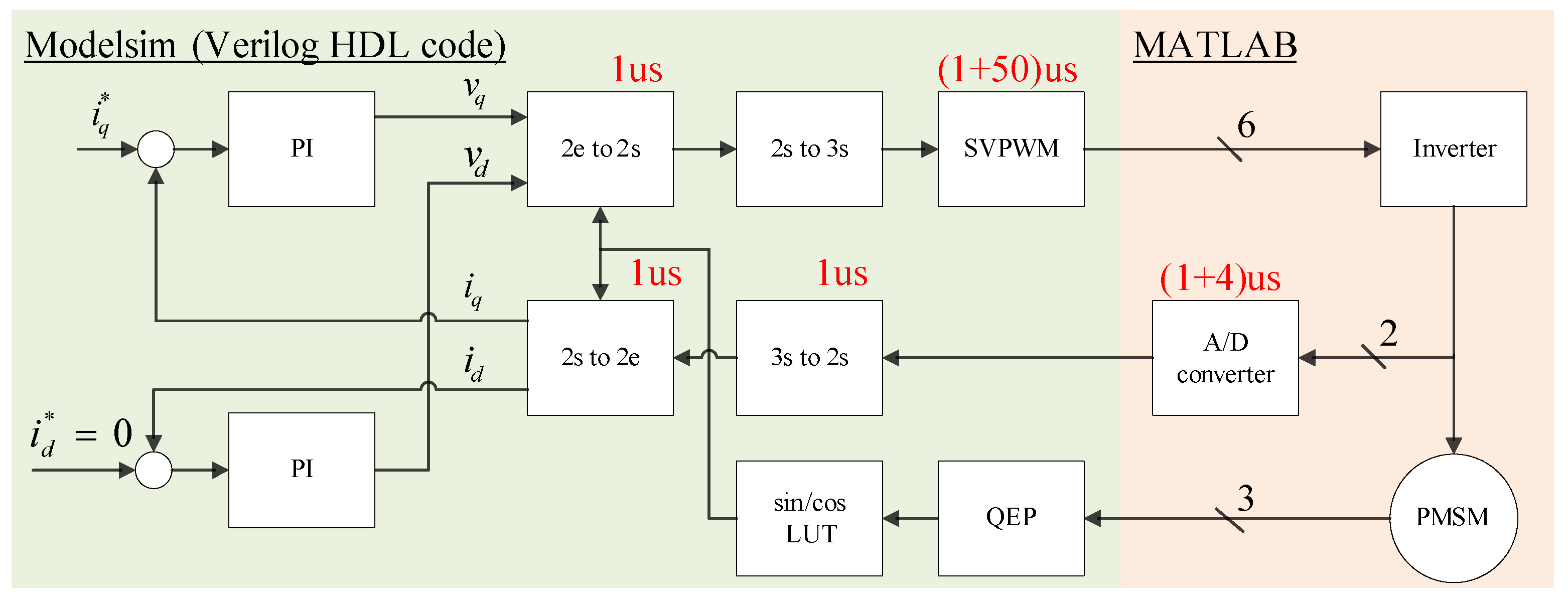
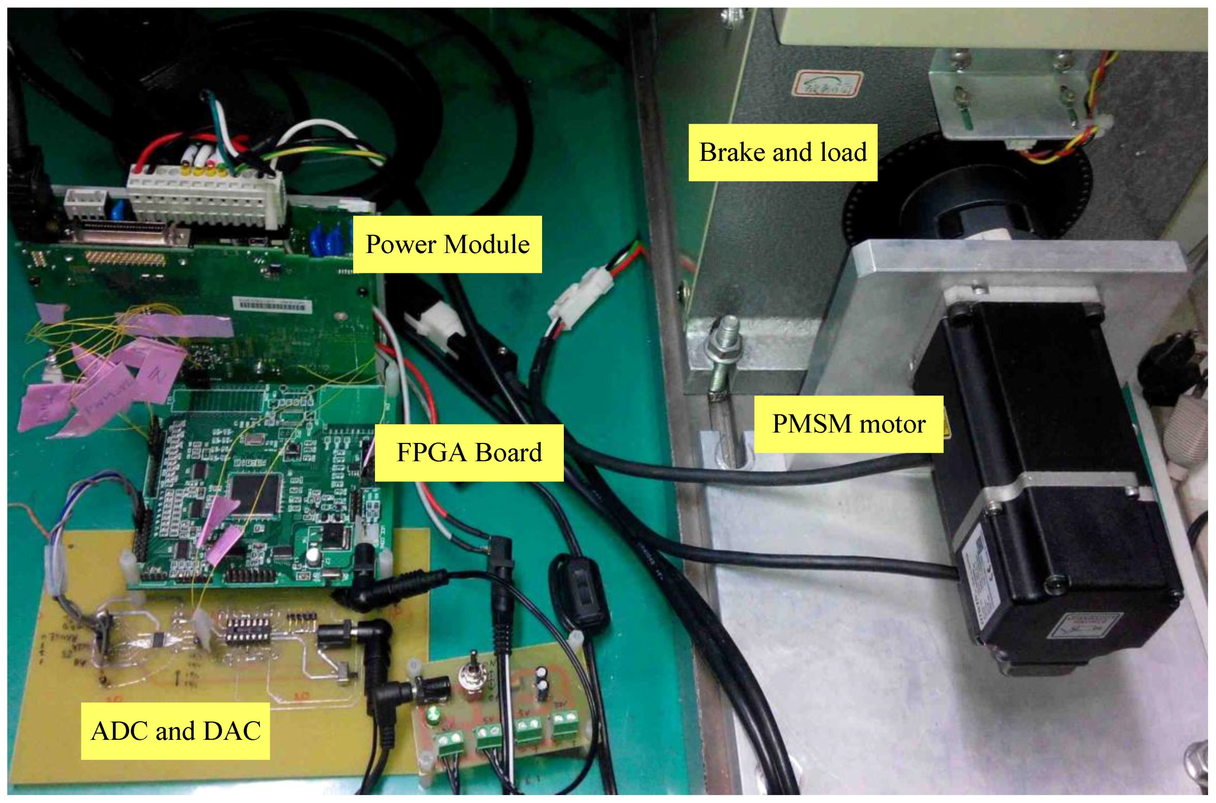
The hardware setup for the implementation of the experiment is shown in Figure 12. It includes an Altera FPGA-based control board, a 12-bit serial ADC and serial DAC board, power module board, brake, and PMSM. Analog currents of phase A and B are sensed by resistors on the power module board without filtering, and are converted into digital values by serial ADCs, AD7866, with unipolar multi-channel voltage input. The ADCs are operated at a 250 kHz sampling frequency, it feeds back the digital values of the winding currents to the controllers in the FPGA by way of the serial to parallel interface. Additionally, the DACs are used to convert the discrete-type control variables (currents of and ) into analog waveforms with the transfer gain of 0.5 V/A, and shown on the digital oscilloscope. Finally, we copy the waveforms on the oscilloscope and plot them in MATLAB. Furthermore, the PMSM motor is shaft-connected to a brake, and rotor is locked by the brake when operating with high-frequency command input.
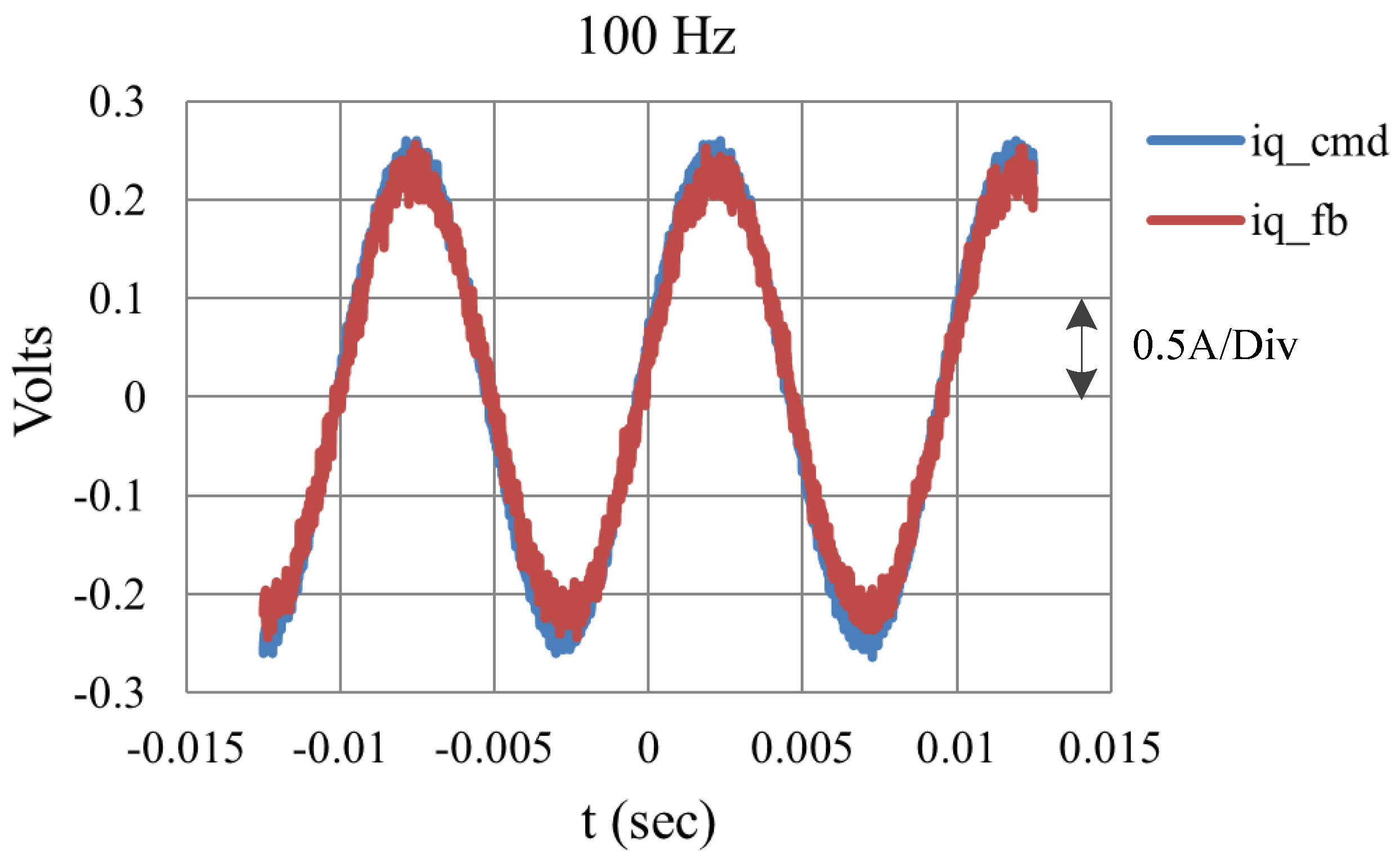
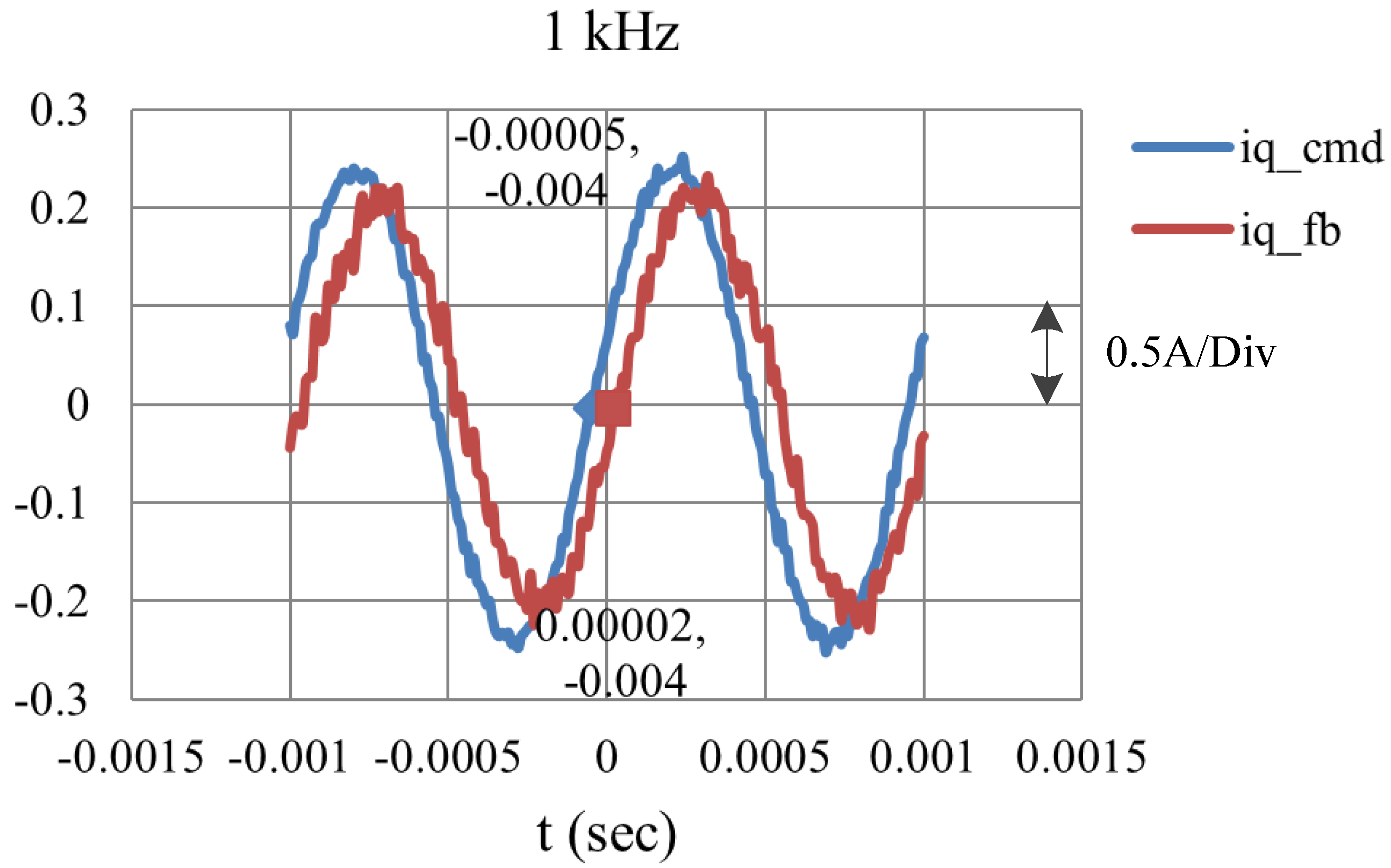
The current commands used in the simulation are also used for the experiment, and only the results of the q-axis currents are shown. Figure 13 shows the result with an amplitude of and a frequency of 100 Hz. It shows that the designed response nearly matches the command without phase delay and amplitude attenuation, i.e., it has good tracking when it is operated at 100 Hz. It is worth noticing that the trigger time of Figure 13 is set at the center of the screen due to the fact that the data in the figure is from the digital oscilloscope. Figure 14 is the result with command 1 kHz. Two points, (−0.00005–0.004) and (−0.00002–0.004), are chosen to evaluate the phase delay and the corresponding result is . This shows that the response has only a slight drop-off in amplitude and a small phase delay compared to the command. Upon comparing the simulated and experimental results, it is also found that they are quite similar to each other. Finally, the experimental results show that the hardware system has attained the expected performance with a bandwidth greater than 1 kHz.
5. Conclusions
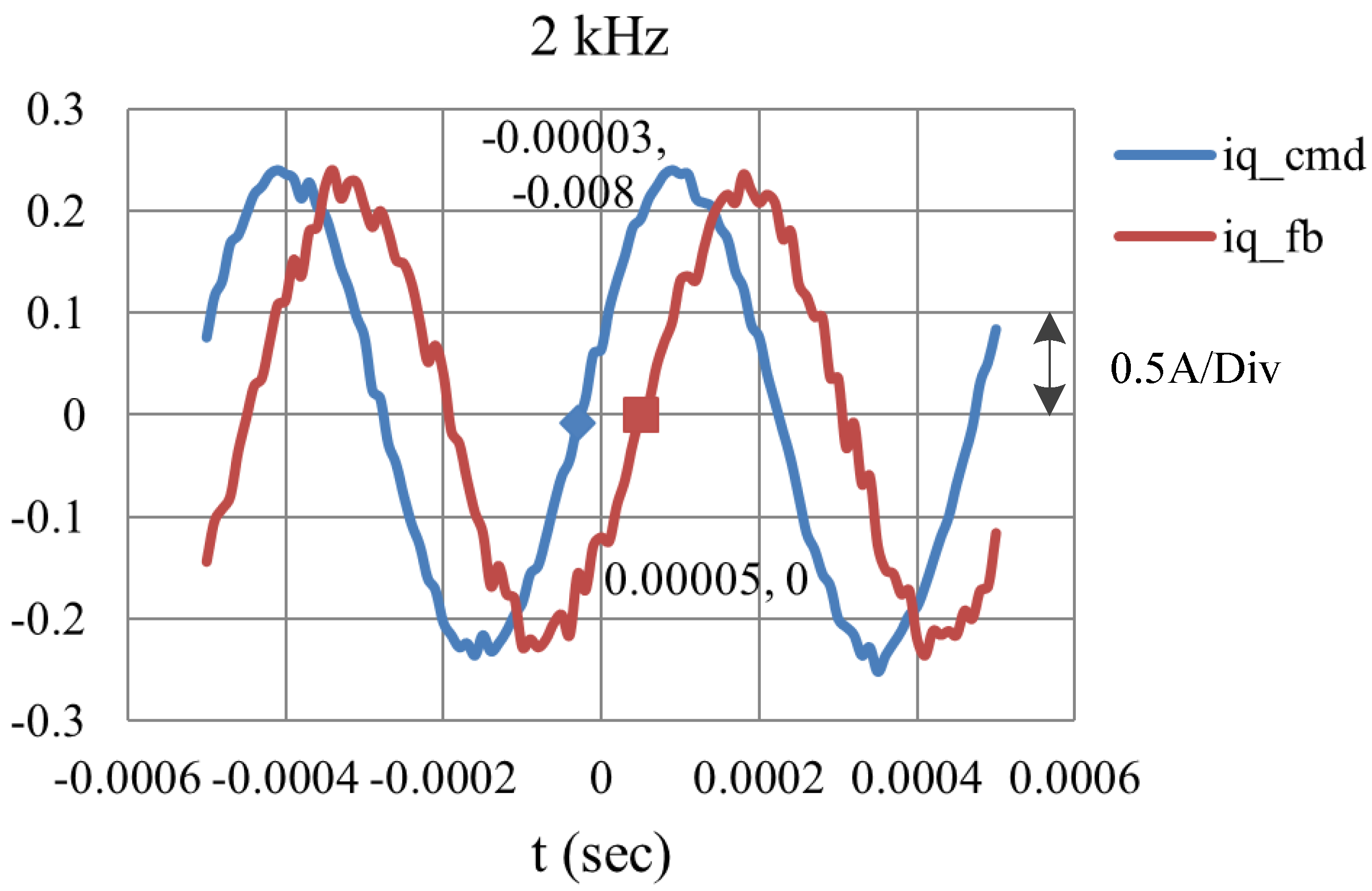
In this paper, we have shown the analysis and hardware current loop controller design with FPGA for a PMSM driver. The design considers the executing and computation delay of the hardware system. The developing procedure starts from the system design with MATLAB/Simulink, and the built model is verified by Modelsim. Moreover, the resulting Verilog HDL codes are modified to fit the selected FPGA. Finally, the developed system is realized on an Altera Cyclone III FPGA, and evaluated by the PMSM drive system. The simulated and practical experimental results show that the developed current loop vector control system with MATLAB/Simulink has been successfully realized, and also reveals a high dynamic response. The bandwidth is greater than 1 kHz. The setup system also successfully operates the current system reaching to 2 kHz as shown in Figure 15, where the response has a phase delay is approximately .
The digital hardware circuits for the controller design are complicated when they are developed directly from the electronic design automation (EDA) system. On the other hand, when the design is started from platforms like MATLAB/Simulink, LabVIEW, or other similar tools, they make the design easy. Of course, it is necessary to optimize the created hardware circuit to make it an usable IP.
Author Contributions
Chiu-Keng Lai and Yao-Ting Tsao conceived and designed the experiments; Yao-Ting Tsao and Chia-Che Tsai performed the experiments; Chiu-Keng Lai, Yao-Ting Tsao, and Chia-Che Tsai analyzed the data; and Chiu-Keng Lai and Yao-Ting Tsao wrote the paper.
Conflicts of Interest
The authors declare no conflict of interest.
References
- Siwakoti, Y.P.; Town, G.E. Design of FPGA-Controlled Power Electronics and Drives Using MATLAB Simulink. In Proceedings of the IEEE/ECCE, Melbourne, VIC, Australia, 3–6 June 2013; pp. 571–577. [Google Scholar] [CrossRef]
- Stumpf, A.; Elton, D.; Devlin, J.; Lovatt, H. Benefits of an FPGA based SRM controller. In Proceedings of the IEEE 9th Conference on Industrial Electronics and Applications (ICIEA), Hangzhou, China, 9–11 June 2014; pp. 12–17. [Google Scholar]
- Rohit, B.C.; Patil, M.D.; Shah, D.; Kadam, A. FPGA Implementation of SVPWM Control Technique for Three Phase Induction Motor Drive Using Fixed Point Realization. In Proceedings of the 2014 International Conference on Circuits, Systems, Communication and Information Technology Applications, Mumbai, Maharashtra, India, 4–5 April 2014; pp. 93–98. [Google Scholar]
- Kung, Y.-S.; Tsai, M.-H. FPGA-Based Speed Control IC for PMSM Drive with Adaptive Fuzzy Control. IEEE Trans. Power Electron. 2007, 22, 2476–2486. [Google Scholar] [CrossRef]
- Kung, Y.-S.; Huang, P.-G.; Chen, C.-W. Development of a SOPC for PMSM Drives. In Proceedings of the 47th IEEE International Midwest Symposium on Circuits and Systems, Hiroshima, Japan, 25–28 July 2004; pp. 329–332. [Google Scholar]
- Quynh, N.V.; Kung, Y.-S. FPGA-Realization of Fuzzy Speed Controller for PMSM Drives without Position Sensor. In Proceedings of the ICCAIS, Nha Trang, Vietnam, 25–28 November 2013; pp. 278–282. [Google Scholar] [CrossRef]
- Zhang, G.Z.; Zhao, F.; Wang, Y.X.; Wen, X.H.; Cong, W. Analysis and Optimization of Current Regulator Time Delay in Permanent Magnet Synchronous Motor Drive System. In Proceedings of the 2013 International Conference on Electrical Machines and Systems, Busan, Korea, 26–29 October 2013; pp. 2286–2290. [Google Scholar]
- Zhang, C.J.; Wu, X.J.; Zuo, X.Y. FPGA Soft-Core Based Step Motor Driving. In Proceedings of the 2010 International Conference on Electrical and Control Engineering, Wuhan, China, 25–27 June 2010; pp. 1035–1038. [Google Scholar]
- Horvat, R.; Jezernik, K.; Curkovic, M. An Event-Driven Approach to the Current Control of a BLDC Motor Using FPGA. IEEE Trans. Ind. Electron. 2014, 61, 3719–3726. [Google Scholar] [CrossRef]
- Kocur, M.; Kozak, S.; Dvorscak, B. Design and Implementation of FPGA-Digital Based PID Controller. In Proceedings of the 15th International Carpathian Control Conference, Velke Karlovice, Czech Republic, 28–30 May 2014; pp. 233–236. [Google Scholar]
- Quang, N.K.; Kung, Y.-S.; Ha, Q.P. FPGA-Based Control Architecture Integration for Multiple-Axis Tracking Motion Systems. In Proceedings of the IEEE/SICE, Kyoto, Japan, 20–22 December 2011; pp. 591–596. [Google Scholar] [CrossRef]
- Data sheet of FRLS4020506A. Available online: https://www.hiwin.de/en/Produktfinder_Detail_2/Motors_Drives_and_Accessories/Servo_motors/Without_motor_brakeand_feather_key/20373 (accessed on 23 October 2017).
Figure 1.
The block diagram of simulated system for PMSM speed control.

Figure 2.
The block diagram of the current vector control.

Figure 3.
The realization of the hardware PI controller.
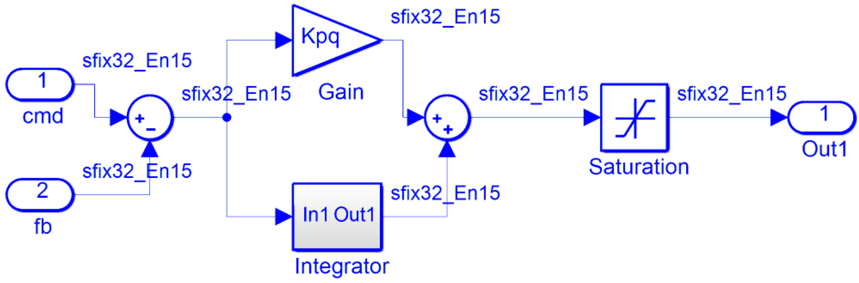
Figure 4.
The SVPWM module.

Figure 5.
The generation of by SVPWM. (a) A vector voltage in Sector 1; and (b) the switching pattern.
Figure 5.
The generation of by SVPWM. (a) A vector voltage in Sector 1; and (b) the switching pattern.

Figure 6.
The vector control system to show the propagation delay.

Figure 7.
The equivalent block diagram of the q-axis closed-loop current control.
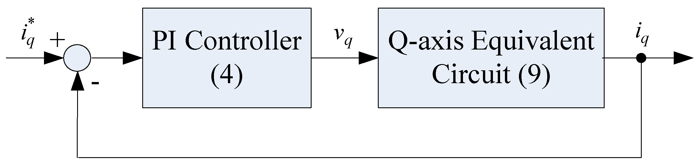
Figure 8.
The frequency response of Equation (14).

Figure 9.
The frequency response of Equation (12).

Figure 10.
The simulated result with 100 Hz sinusoidal command. (a) q-axis current command and response; and (b) d-axis current command and response.
Figure 10.
The simulated result with 100 Hz sinusoidal command. (a) q-axis current command and response; and (b) d-axis current command and response.


Figure 11.
The simulated result with 1 kHz sinusoidal command. (a) q-axis current command and feedback; and (b) d-axis current command and feedback.
Figure 11.
The simulated result with 1 kHz sinusoidal command. (a) q-axis current command and feedback; and (b) d-axis current command and feedback.

Figure 12.
The setup of the experimental system.

Figure 13.
The experimental result with a 100 Hz sinusoidal input.

Figure 14.
The experimental result with a 1 kHz sinusoidal input.

Figure 15.
The experimental result with a 2 kHz sinusoidal command.


Table 1.
The parameters of PMSM motor (FRLS 4020506A).
| Pole | 10 |
|---|---|
| 3.5 | |
| 13 | |
| 0.270 | |
| 0 | |
| 0.0707 | |
| 1.27 |
© 2017 by the authors. Licensee MDPI, Basel, Switzerland. This article is an open access article distributed under the terms and conditions of the Creative Commons Attribution (CC BY) license (http://creativecommons.org/licenses/by/4.0/).
Share and Cite
MDPI and ACS Style
Lai, C.-K.; Tsao, Y.-T.; Tsai, C.-C. Modeling, Analysis, and Realization of Permanent Magnet Synchronous Motor Current Vector Control by MATLAB/Simulink and FPGA. Machines 2017, 5, 26. https://doi.org/10.3390/machines5040026
AMA Style
Lai C-K, Tsao Y-T, Tsai C-C. Modeling, Analysis, and Realization of Permanent Magnet Synchronous Motor Current Vector Control by MATLAB/Simulink and FPGA. Machines. 2017; 5(4):26. https://doi.org/10.3390/machines5040026
Chicago/Turabian StyleLai, Chiu-Keng, Yao-Ting Tsao, and Chia-Che Tsai. 2017. "Modeling, Analysis, and Realization of Permanent Magnet Synchronous Motor Current Vector Control by MATLAB/Simulink and FPGA" Machines 5, no. 4: 26. https://doi.org/10.3390/machines5040026
Note that from the first issue of 2016, this journal uses article numbers instead of page numbers. See further details here.