Size Effect and Deformation Mechanism in Twinned Copper Nanowires
by
 , ,
, ,
Jiapeng Sun
1,* ,
,
Cheng Li
1,
Jing Han
2,
Xiaoyan Shao
3,
Xiaowei Yang
1,
Huan Liu
1,
Dan Song
1 and
Aibin Ma
1,* 1
College of Mechanics and Materials, Hohai University, Nanjing 210098, China
2
School of Mechanical and Electrical Engineering, China University of Mining and Technology, Xuzhou 221116, China
3
School of Engineering and Technology, China University of Geosciences, Beijing 100083, China
*
Authors to whom correspondence should be addressed.
Metals 2017, 7(10), 438; https://doi.org/10.3390/met7100438
Submission received: 30 August 2017
/
Revised: 5 October 2017
/
Accepted: 16 October 2017
/
Published: 18 October 2017
Abstract
:Molecular dynamics simulations were performed to demonstrate the synergistic effects of the extrinsic size (nanowire length) and intrinsic size (twin boundary spacing) on the failure manner, yield strength, ductility and deformation mechanism of the twinned nanowires containing high density coherent twin boundaries CTBs paralleled to the nanowires’ axis. The twinned nanowires show an intense extrinsic size effect, i.e., shorter is stronger and more ductile, and an intense intrinsic size effect, i.e., thinner is stronger. Notably, the strengthening effect degradation of CTBs in the twinned nanowires is observed with an increase in nanowire length: remarkable strengthening effect can be obtained for the short nanowires, but the strengthening effect becomes less pronounced for the long nanowires. The twinned nanowires fail via a ductile manner or via a brittle manner depending on the synergistic effect of the nanowire length and twin boundary spacing. By atomic-level observation of the plastic deformation, we found that the emission of a trailing 30° partial from the free surface controls the yield behavior of the twinned nanowires. We also found that the special zigzag extended dislocations are formed by the dislocation–CTBs interactions, and propagate to sustain the plastic deformation.
1. Introduction
Nanotwinned metallic materials, comprised of coherent twin boundaries (CTBs) with nanometer-scale spacing, have been paid special attention since firstly reported by Lu et al. [1] because of the unusual combination of ultra-high strength (on the order of 1 GPa for the nanotwinned Cu vs. 0.25 GPa for the coarse-grained Cu) and high tensile ductility (up to 14% for the nanotwinned Cu) [2,3,4], along with considerable work hardening [4,5,6]. Both experiments [7,8,9] and molecular dynamics (MD) simulations [2,10,11,12,13] revealed that the novel mechanical properties of the nanotwinned metals originate from the size-dependent dislocation–CTB interactions. Hence, engineering CTBs into the metals has become an attractive strategy of simultaneously strengthening and toughening metal.
Likewise, when the abundant CTBs are engineered into the face-centered cubic (FCC) metals nanowires or nanopillars, the extreme-high strength and even the ideal strength can be achieved [14,15]. Interestingly, the desired strain-hardening capability in low stacking-fault energy metals such as Au and Ag [16,17,18] also can be obtained by the CTBs, which is always missing in single crystal metal nanowires or nanopillars [19,20,21]. The twinned nanowires containing orthogonally oriented CTBs have received much research attention during the last decade. The experiments and MD simulations revealed that the tensile strength of twinned Cu nanopillars is up to 2.5 GPa, as about 1.5 times higher as the single crystal counterpart [14]. The twinned Au nanowires containing angstrom-scaled twins (0.7 nm in thickness) exhibit tensile strength up to 3.12 GPa, near the ideal strength [15]. The extremely high strength of the twinned nanowires is due to the additional repulsive force exerted by CTBs on the dislocation nucleation and glide [22,23,24,25]. The strength of the twinned nanowires is observed to scale with the twin boundary spacing, indicating a remarkable intrinsic size effect [23,25,26,27], and is also linked to the geometry size of the nanowires, showing an extrinsic size effect [14]. The failure manner, ductile or brittle manner, is proved to depend on twin boundary spacing and geometry size [12,14]. The twinned nanowires containing orthogonally oriented CTBs yield via the emission of dislocation from CTB–surface intersection sites [23], which is very different from the twin free nanowires. Moreover, the novel mechanical properties and deformation mechanism can be linked to the dislocation–CTB interactions, and the different dislocation–CTB interactions lead to remarkable or missing strain-hardening behavior in different metals’ nanowires [17].
Compared with the rich investigations on the twinned nanowires containing orthogonally oriented CTBs, little attention has been paid on the twinned nanowires containing parallel-oriented CTBs and slant-oriented CTBs. Recently, Lu et al. [28] explored the correlation between CTB orientation, active slip systems and dislocation structure examined by TEM. The result revealed that the dislocation slip mode and dislocation–CTB interactions are significantly related to the CTB orientation. The MD simulations demonstrated that the dominant deformation mechanism transits dynamically from slip transfer to twin boundary migration to slip-twin interactions as the twin boundary orientation changes from horizontal to slant, and then to a vertical direction [29]. Therefore, the CTB orientation-dependent mechanical behavior and deformation mechanism have not been fully understudied, which are crucial in advancing the understanding of plastic anisotropy of twinned nanowires, and helpful to develop the polycrystalline nanotwinned metals with randomly oriented CTBs. Moreover, the twinned nanowires provide an ideal model system in which the elaborate control of nanostructure processing and characterization facilitates a direct coupling between experiments and modeling [13].
In this work, we applied MD simulations to investigate the mechanical behavior of the twinned Cu nanowires containing high density CTBs parallel to the nanowires axis under uniaxial tensile load, which is different from the commonly reported twinned nanowires containing orthogonally oriented CTBs [12,14,18,25,30]. We focused on the synergistic effects of the extrinsic size and intrinsic size on the failure manner, yield strength, ductility and deformation mechanism of the twinned nanowires, as well as the single crystal nanowires. The dislocation emission and dislocation–CTB interactions during plastic deformation were analyzed by the atomic-level observation to reveal the yield mechanism and the special zigzag extended dislocation.
2. Simulation Methodology
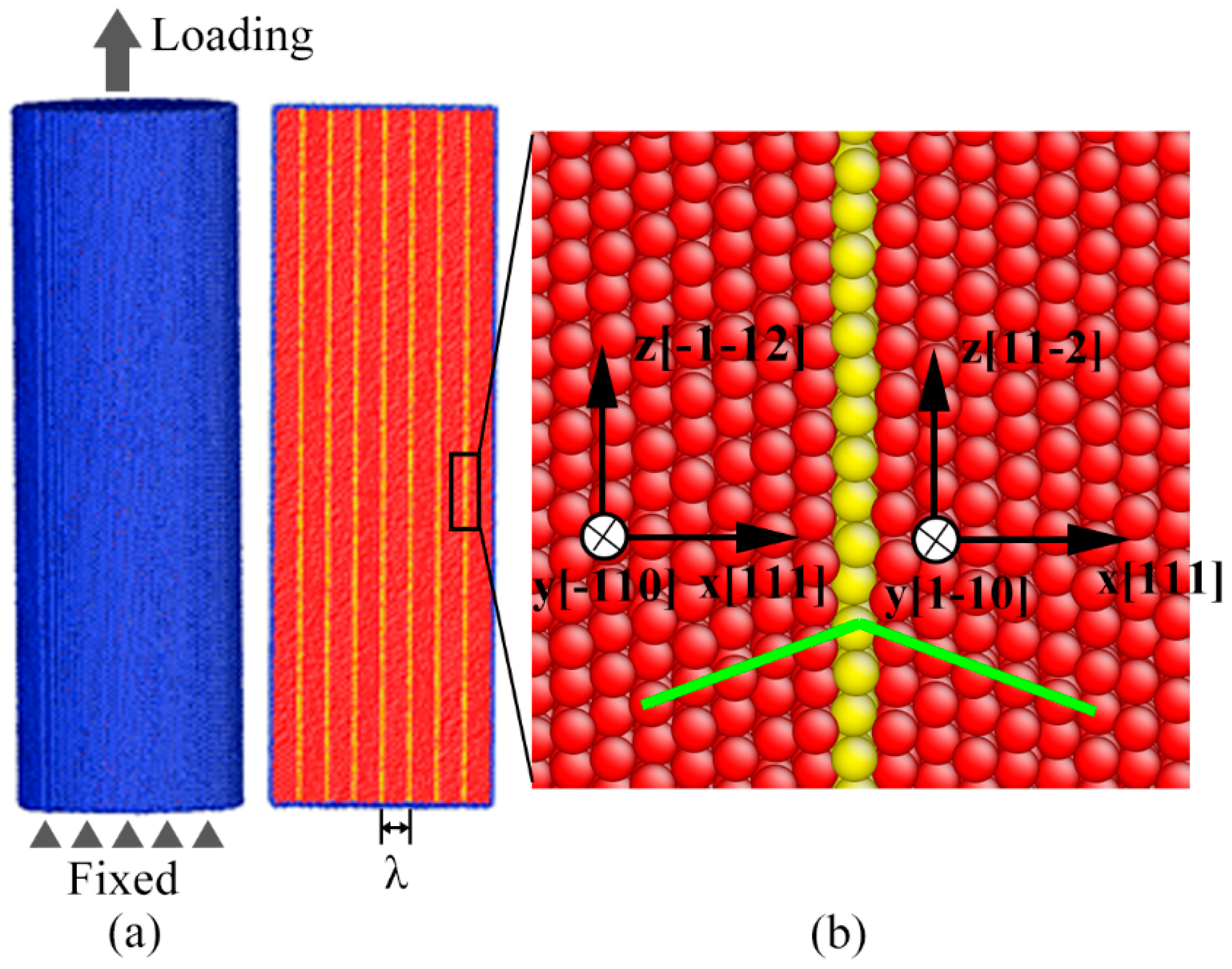
Large-scale molecular dynamics (MD) simulations were performed with an embedded atom-method potential [31]. The cylindrical nanowires were constructed by periodically repeating ∑3 CTBs with their long axis oriented in the [-1-12] direction in the matrix or the [11-2] direction in twin, as illustrated in Figure 1. The nanowire diameter d was 15 nm, and their initial lengths L0 ranged from 15 nm to 450 nm. The nanowires maximally consisted of ~6,900,000 atoms. The twin boundary spacing λ (i.e., the spacing between adjacent CTBs) was chosen from a range between 0.63 nm and 2.5 nm. The free boundary conditions were imposed along all directions, indicating the finite length nanowires. The atoms in a layer with a thickness of 1 nm at one end of the nanowires were frozen to provide structural stability. The uniaxial tension was simulated by displacing the atoms in a layer with thickness of 1 nm at the other end of the nanowires at a constant velocity.
To suppress the oscillation of the axial stress led by the low frequency but long-lived oscillations associated with the free boundary, a meticulous heat treatment process was performed. The initial nanowires were firstly heated from 0 K to 300 K over 100 ps, and then annealed at 300 K for 200 ps under the NVT ensemble using a Nosé–Hoover temperature thermostat [32,33]. After the nanowires were equilibrated, the uniaxial tensile loading was applied by stretching the nanowires in the axial direction at a constant strain rate of 0.5 ns−1 and at a temperature of 300 K. The Viral theorem and deformed atomic volume were used to calculate the axial stress. Common neighbor analysis (CNA) [34] and slip vector analysis (SVA) [35] were used to identify defects during deformation. All of the MD simulations were performed utilizing the Verlet integration algorithm with a time step of 1 fs by large-scale atomic/molecular massively parallel simulator (LAMMPS) [36].
3. Results and Discussion
3.1. Length Dependent Stress–Strain Behavior
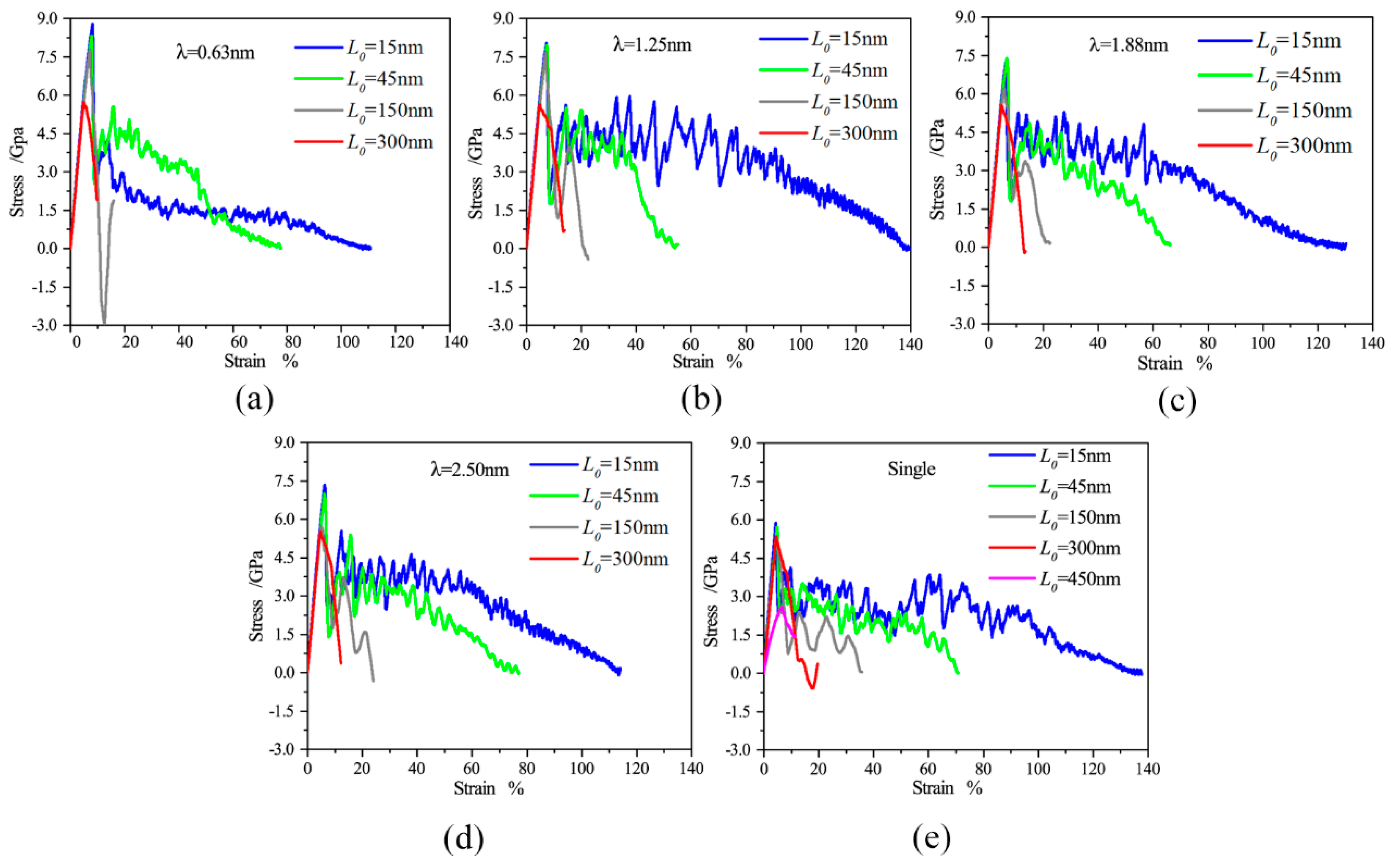
Figure 2a–d show the length dependent stress–strain curves of the twinned Cu nanowires with λ = 0.63 nm, 1.25 nm, 1.88 nm, and 2.5 nm. For comparison, the stress–strain curves of the <11-2> oriented single crystal Cu nanowires are also shown in Figure 2e. A key result is that all of the nanowires fall into two modes fracture, ductile and brittle manner. In the ductile manner, the nanowires with small L0 (L0 < 300 nm for twinned Cu nanowires and L0 < 450 nm for single crystal Cu nanowires) exhibit significant serrated stress–strain curves, indicating extensive plasticity. The ductility, indexed by elongation to failure, dramatically increases with decreasing nanowire length, accompanying with the increasing serrations in the stress–strain curves. In a brittle manner, the twinned nanowires with L0 = 300 nm and the single crystal nanowires with L0 = 450 nm fracture at the first stress drop, suggesting small elongation to failure. More work demonstrates that the longer nanowires all fail via a brittle manner. This result indicates that the twinned Cu nanowires undergo a ductile-to-brittle transition with an increase in the nanowire length regardless of the twin boundary spacing, as well as single crystal Cu nanowires. In other words, the short nanowires fail via a ductile manner with extensive ductility, while long nanowires fail via a brittle manner with seldom ductility. The length dependent ductile-to-brittle transition has been reported for the [111] oriented single crystal Cu, Au nanowires [37,38] and the twinned Cu nanowires containing orthogonally oriented CTBs [12].
As commonly reported in literature [17,18,38,39,40], the serrations in the stress–strain curve are the typical characteristic of the metal nanowires, and are resulted by the sequential occurrences of dislocations bursts activated on different slip systems. Moreover, we found that the flow stress of the ductile nanowires slowly decreases in the initial stage of plastic deformation reflected by sparse and large amplitude serrations, and subsequently rapidly decreases until failure reflected by dense and small amplitude serrations in stress–strain curves, as shown in Figure 2.
3.2. Twin Boundary Spacing Dependent Stress–Strain Behavior
Compared the Figure 2a–d, it is found that twin boundary spacing also has strong impacts on the plastic deformation and the failure mode of the twinned nanowires. The stress–strain behaviors of the twinned nanowires with L0 = 45 nm, 200 nm, 300 nm are illustrated in Figure 3, as related to twin boundary spacing. As shown in this figure, the short twinned Cu nanowires (L0 = 45 nm) all fail via a ductile manner, and the long nanowires with L0 = 300 nm fail via brittle manner, no matter what the twin boundary spacing is. In contrast, the intermediate-long nanowires with L0 = 200 nm undergo a ductile-to-brittle transition with a decrease in twin boundary spacing. This demonstrates that the failure mode transition depending on the twin boundary spacing can be found just for the intermediate-long twinned nanowires rather than the short nanowires or the long nanowires.
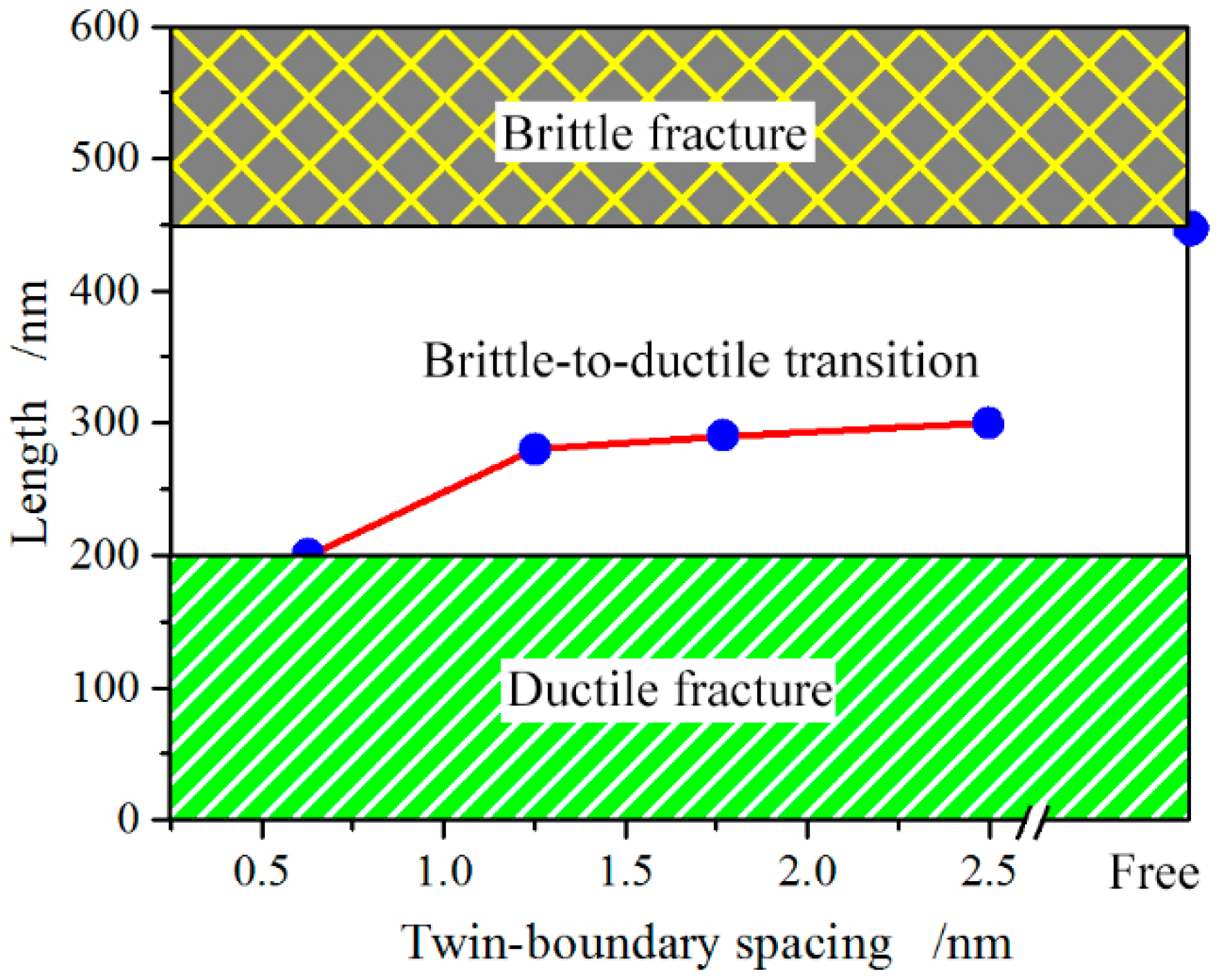
The present results emphasize that the mechanical behavior and the ductile-to-brittle transition of the twinned Cu nanowires not only depend on their extrinsic characteristic size (i.e., the length of nanowires), but also intensely relate to their intrinsic characteristic size (i.e., twin boundary spacing). To address this issue, additional MD simulations were performed to find the critical length for the failure mode transition. The resulted failure modes related to both nanowire length and twin boundary spacing are illustrated in Figure 4, which is called the fracture map of the twinned Cu nanowires. This figure can be separated into three regions according to the nanowires’ length. While we check the twin boundary spacing effect on the failure mode, the long nanowires (L0 > 450 nm) always show brittle failure (brittle fracture region), and the short nanowires (L0 < 200 nm) invariably fail in a ductile manner (ductile fracture region) regardless of the twin boundary spacing. In contrary, the ductile-to-brittle transition depending on the twin boundary spacing, labeled as ductile-to-brittle transition in Figure 4, can just be detected in a length range of 200 nm to 450 nm. In other words, if we examine the role of the twin boundary spacing in the fracture behavior at a given length that is just in the range of 200 nm to 450 nm, a ductile-to-brittle transition will be detected with a decrease in the twin boundary spacing, while only brittle failure for the long nanowires and ductile failure for the short nanowires can be observed beyond this range. On the contrary, while we check the length effect on the failure mode, the ductile-to-brittle transition is always observed and is independent of the twin boundary spacing.
The critical length for the failure mode transition increases with an increase in the twin boundary spacing, as shown in Figure 4. When the twin boundary spacing decreases from 2.5 nm to 1.25 nm, the critical length slightly shrinks from 300 nm to 280 nm. However, sudden reduction in critical length occurs when the twin boundary spacing approaches its minimum of 0.63 nm in which just single atomic layer lies between two CTBs. The sudden reduction and subsequent slow decrease in the critical length were observed for the twinned Cu nanowires containing orthogonally oriented CTBs, in which the sudden reduction occurs when the twin boundary spacing decreases blow to 3.76 nm [12]. We thus conclude that the high density CTBs facilitate the brittle failure for the nanowires.
3.3. Intrinsic and Extrinsic Size Effect
The small-scale metallic material exhibits now-commonly-known “intrinsic size effect” and “extrinsic size effect” [21], i.e., “smaller is stronger”. The intrinsic size is generally regarded as the internal characteristic microstructural length scale, such as, grain or precipitate size, twin boundary spacing, or dislocation density. As the name implies, the extrinsic size refers to the test sample size, such as the nanowire length and diameter, the thickness of thin film, and the diameter of the nanopillar. For the present twinned Cu nanowires, the only intrinsic size is the twin boundary spacing, and the extrinsic size includes the diameter and length of the nanowires.
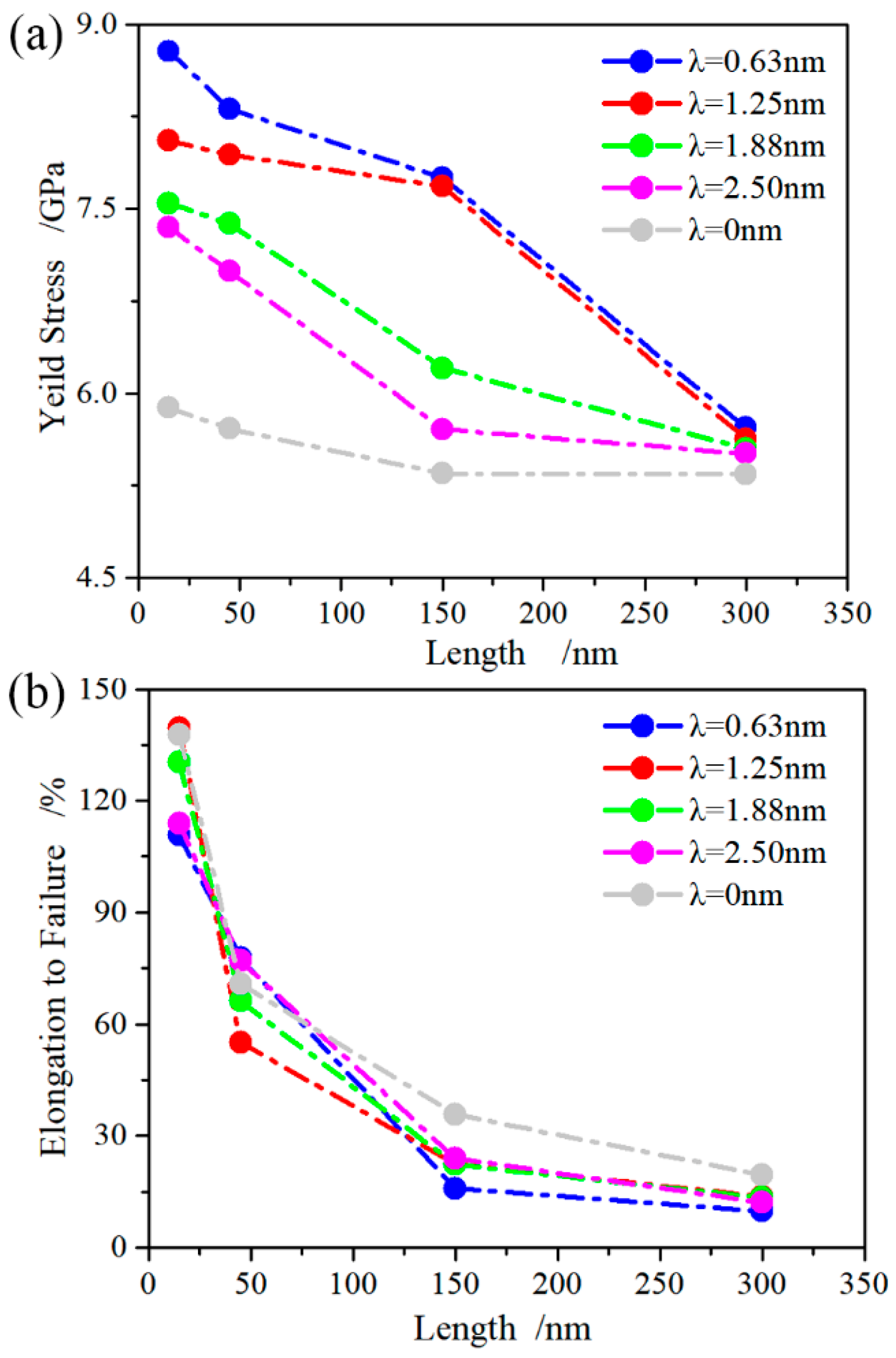
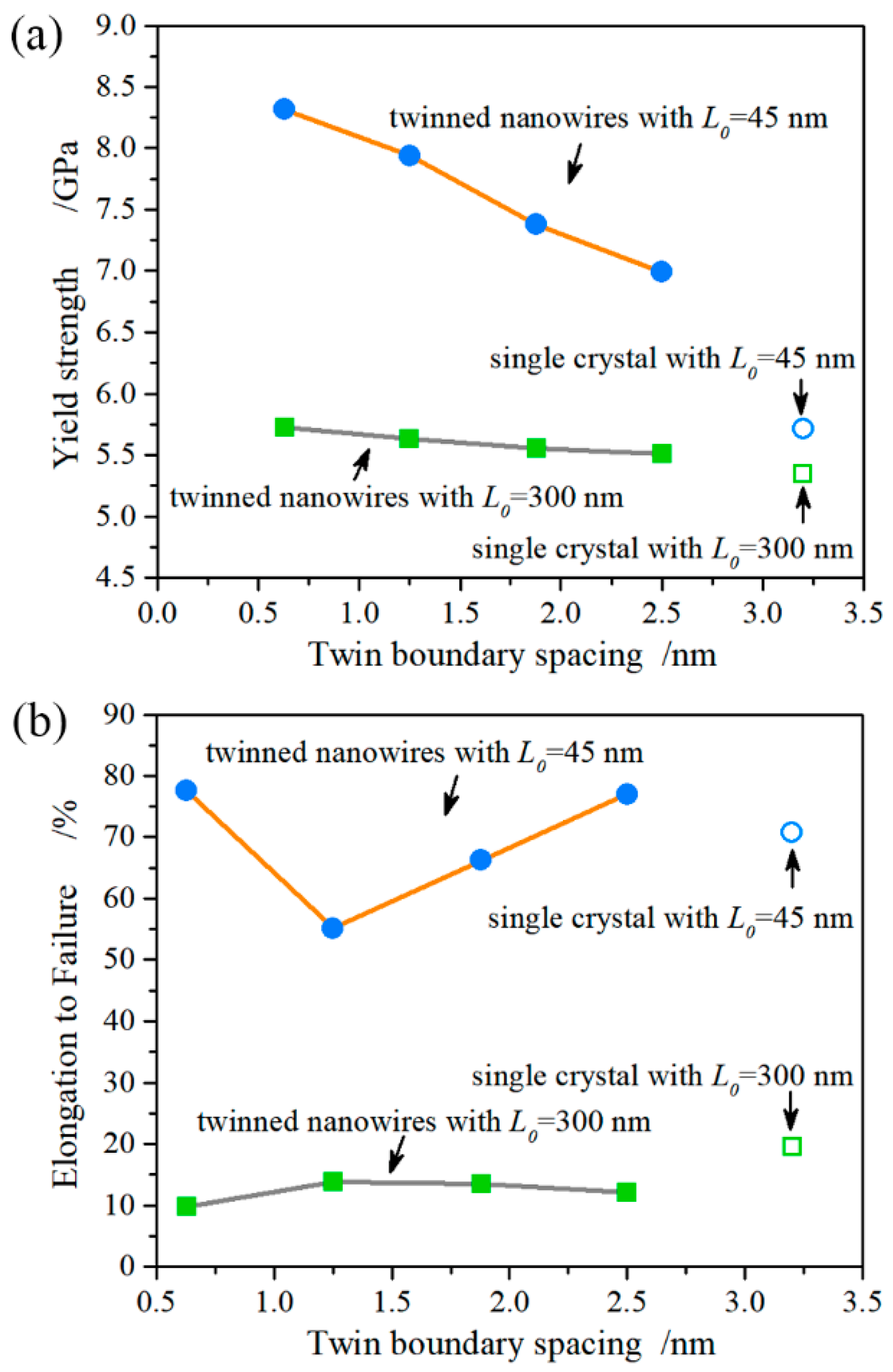
We firstly focus on an extrinsic size effect. The yield strength and elongation to failure of the twinned Cu nanowires rapidly increase with a decrease in nanowire length, indicating “shorter is stronger and more ductile”, as well as single crystal nanowires, as shown in Figure 5. Compared with the single crystal nanowires, the twinned nanowires show a relatively high degree of yield stress decrease, as shown in Figure 5a. Taking the twinned Cu nanowire with λ = 1.88 nm as an example, the yield strength decreases from 8.78 GPa to 5.72 GPa (34.85% reduction), compared with the insignificant decrease from 5.88 GPa to 5.34 GPa (9.18% reduction) for the single crystal nanowires, when the nanowire length increases from 15 nm to 300 nm. This indicates that the twinned nanowires exhibit stronger length-dependent size effect than the single crystal nanowires.
Turning to the intrinsic size effect, Figure 6a shows clear evidence that the yield strength of the twinned nanowires increases with a reduction in twin boundary spacing, indicating strong intrinsic size effect, i.e., thinner is stronger. The linear dependence of the yield strength on the twin boundary spacing is observed: σs∝-0.73λ for the short nanowires with L0 = 45 nm, and σs∝-0.12λ for the long nanowires with L0 = 300 nm. This indicates that the short nanowires exhibit a relatively strong intrinsic size effect compared with the long nanowires. A 45.51% increase in yield strength is obtained for the twinned nanowires with L0 = 45 nm, but just a small increase of 7.10% for the long twinned nanowires with L0 = 300 nm is shown relative to the single crystal nanowires. We thus concluded that the strengthening effect of high density CTBs is significantly modulated by the nanowire length: remarkable strengthening effect can be obtained for the short nanowires, but the strengthening effect becomes less pronounced for the long nanowires. The significant strengthening effect of CTBs has been ubiquitously found for the FCC metallic nanowires or nanopillars with a small length both in experiments and MD simulations [12,14,15,25,40,41,42]. To the authors’ knowledge, the strengthening effect degradation of CTBs with an increase in the nanowire length has never been reported, which should be paid special attention to for developing the nanotwinned metal and designing nanoscale mechanical systems.
Compared with the strengthening effect of CTBs, the CTBs have a weak influence on the elongation to failure of the nanowires, as shown in Figure 6b. For the short nanowires with L0 = 45 nm, the statistical relationship between elongation to failure and the twin boundary spacing is not found. For the nanowires with L0 = 300 nm, the elongation to failure is smaller than that for the single crystal nanowires, indicating the unfavorable effect of CTBs on the ductility. Additional MD simulations indicate that the CTBs have an unfavorable effect on the ductility when the nanowire length is larger than 100 nm.
3.4. Atomic-Level Observations of Yield and Deformation Mechanism
The yield and deformation mechanism of the twinned Cu nanowires were investigated by the atomistic snapshots. Taking the twinned Cu nanowires with L0 = 45 nm and λ = 1.88 nm as an example, the first plasticity event is facilitated by the emission of a 30° partial Cβ associated with the formation of a stacking fault at the strain of 6.40%, as shown in Figure 7a. The first dislocation nucleates from the site between adjacent CTBs on the free surface. For twinned nanowires containing orthogonally oriented CTBs, dislocation nucleation from the intersection sites between the free surface and CTBs, where the high stress gradient is achieved, is believed to be responsible for the yield behavior [14,23,25]. This result highlights the CTB orientation dependent plasticity mechanism.
Notably, the onset of the first dislocation at the strain of 6.40% is not accompanied by the occurrence of the yield in the stress–strain curves at the strain of 6.60%. Due to the small twin boundary spacing, the first 30° partial Cβ glides on the ACD plane and is immediately blocked by the CTBs after nucleation. Increasing the strain, the partial dislocation transmits across the CTB, having the following dislocation reaction to release another partial in the twin:
where CβT is a partial that can slip away in the twin from the CTB on the ACDT plane. βTβ is a stair-rod dislocation. After the dislocation reaction, the dislocation configuration is shown in Figure 7b, which displays two stacking faults from the two sides of the CTB meeting at the CTB and connected by the dislocation βTβ.
Cβ → CβT + βTβ,
When the strain increases to 6.60%, a trailing 30° partial βA nucleates following the 30° partial Cβ on the free surface, accompanied by the occurrence of yield. The dislocation glide of the partial βA on the ACD plane eliminates the stacking faults through the following dislocation reaction:
where CA is a perfect dislocation. After this dislocation reaction, an extended dislocation is formed, as shown in Figure 7c.
βA + Cβ → CA,
The trailing partial βA can also transmit across the CTB by the dislocation reaction:
where βTA is a partial that can slip away in the twin from the CTB on the ACDT plane. ββT is a stair-rod dislocation, which is the opposite sign dislocation of βTβ. In the twin, the glide of the partial βTA on the ACDT plane eliminates the stacking fault by the dislocation reaction:
and the stair-rod dislocation βTβ formed by reaction (1) is removed by the dislocation ββT. The overall dislocation reaction processes at the CTBs can be obtained by adding the Reactions (1) and (3):
βA → βTA + ββT,
βTA + CβT → CA,
CA → CTAT.
It means that a perfect screw dislocation CA transmits across CTB, and further glides on the ACDT plane in the twin leaving nothing on the CTB.
As a result, dislocation configurations are displayed in Figure 7c, which show two extended dislocations from the two sides of the CTB meeting at the CTB. Similar dislocation reactions continually process with an increase in strain. Thus, the zigzag extended dislocations connected by the CTBs are formed, as displayed in Figure 7d. The propagation of the zigzag extended dislocations is responsible for the further plastic deformation of the twinned nanowires, which is very different from the activation and sliding of the leading partial and subsequent trailing partial in the single crystal nanowires [37,38,43].
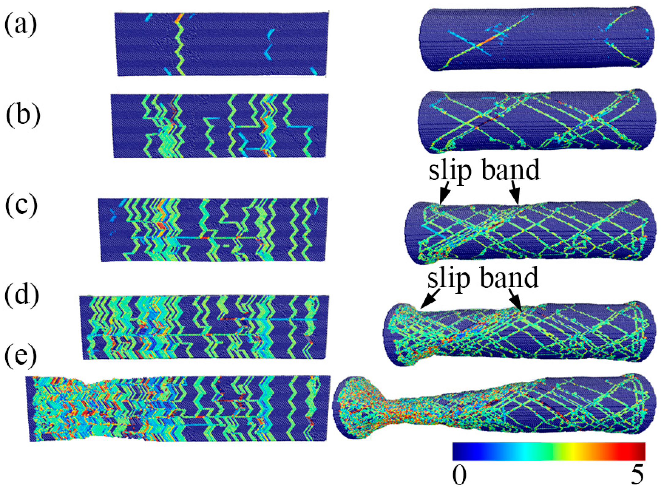
As an increase in the strain, the initial zigzag extended dislocation continually propagates and traverses the nanowires, leaving a corrugated pattern in the cross-section view and a slip line in the full view of the twinned nanowires, as shown in Figure 8a. Simultaneously, the other slip system is activated, which is reflected by the intersected slip lines, as shown in Figure 8a,b. By calculating the Schmid factor, two slip systems, (-11-1) <-2-11> and (1-1-1) <-1-21>, can operate in the twinned nanowires and its single crystal counterpart. The later active 30° partial Cα can also transmit across the CTBs and generates the zigzag extended dislocations due to the dislocation–CTB interactions similar to 30° partial Cβ as discussed previously. Increasing the strain, dislocations homogeneously nucleate at different location on the surface, and move along the two slip systems, creating many shear facets over a large region of the nanowires, as shown in Figure 8b. The intersection of the two slip lines along different slip systems generates large steps on the surface, causing large stress concentration. Thus, dislocations preferentially nucleate at the intersection sites, and subsequently two slip bands on the surface are observed as the tension processes, as shown in Figure 8c. The developing of the slip bands facilitates the localized deformation, which results in the failure of the nanowires, as shown in Figure 8d,e. The localized deformation is further demonstrated by the continually increased dislocation slip concentrated on the left part of the nanowires when the strain increases from 8.25% to 49.5%, as shown in Figure 8b–e.
3.5. Mechanism of Intrinsic and Extrinsic Size Effects
The present results show that the yield strength of the twinned nanowires increases with a reduction in twin boundary spacing, and is always higher than its single crystal counterpart, indicating significantly strengthening effect of CTBs. We demonstrated that the onset of plastic deformation is facilitated by the emission of a trailing 30° partial βA from the site between adjacent CTBs on the free surface for the present twinned nanowires containing parallelly oriented CTBs. It is well known that CTBs can serve as barriers, hindering the dislocation nucleation and glide in nanometals. The hindering effect can be quantitatively described by the image repulsive force exerted by CTBs on the dislocation nucleation and glide [22,23,24,25]. Therefore, the intrinsic size effect observed in the twinned nanowires containing parallel-oriented CTBs can be interpreted by the additional image repulsive force. This repulsive force is helpful for increasing the yield strength of the twinned nanowires, and increases with a decrease in the twin boundary spacing. For twinned nanowires containing orthogonally oriented CTBs, dislocation nucleation at the intersection sites between the free surface and CTBs is responsible for the yield behavior [14,23,25]. Therefore, the strengthening to softening transition exists when the twin boundary spacing is above a critical value because of the competition between the repulsive force and dislocation source number [25]. On the contrary, the source number is not changed with the twinned boundary spacing for the present twinned nanowires containing parallel-oriented CTBs. Hence, only the strengthening effect can be observed for the present twinned nanowires.
With the nanowire length increasing, the dislocation source number increases linearly. If all of the sources are equivalent and share the same probability of nucleating dislocations, the yield strength will increase with a decrease in the nanowire length. The reason for the increase in the yield strength is that, when the number of nucleation sources is small, it is less likely that atomic clusters with enough energy to initiate plastic deformation will be present. Therefore, the change in dislocation source number is responsible for the present observed extrinsic size effect of the twinned nanowires containing parallel-oriented CTBs. This source controlled size effect was observed in twinned nanowires containing orthogonal-oriented CTBs [25]. It is noted that the source controlled size effect is also applicable to the single crystal nanowires. The difference between the twinned nanowires and single crystal nanowires lies in the source number depending on the nanowires length, which is responsible for the relatively weak extrinsic size effect of the single crystal nanowires. In a word, the image repulsive force caused by CTBs is responsible for the intrinsic size effect, and the change in dislocation source number accounts for the extrinsic size effect of the twinned nanowires containing parallel-oriented CTBs. In further work, the quantitative mode of intrinsic and extrinsic size effects will be inferred and discussed in detail.
4. Conclusions
In this paper, the synergistic effects of the extrinsic size and intrinsic size on the failure manner, strength, ductility, and the deformation mechanism of the twinned Cu nanowires were addressed by MD simulations. The cylindric twinned Cu nanowires were constructed containing high density CTBs paralleled to the nanowires’ axis. Our simulation results reveal that the mechanical behaviors of the twinned Cu nanowires are significantly related to the synergistic effects of the nanowire length and twin boundary spacing, indicating strong intrinsic and extrinsic size effects on strength, ductility and failure manner. The twinned nanowires fail via a ductile manner or via a brittle manner, which depends on the synergistic effect of the nanowire length and twin boundary spacing. With increasing the twin boundary spacing, the critical length for the ductile-to-brittle transition increases from 200 nm to 300 nm, which is much smaller than that of 450 nm for the single crystal nanowires. The twinned nanowires show an intense extrinsic size effect, i.e., shorter is stronger and more ductile, and an intense intrinsic size effect, i.e., thinner is stronger. Notably, a strengthening effect degradation of CTBs in the twinned nanowires is observed with an increase in nanowire length: a remarkable strengthening effect can be obtained for the short nanowires, but the strengthening effect becomes less pronounced for the long nanowires. By atomic-level observation of the initial stages of plastic deformation, we found that the emission of a trailing 30° partial from the free surface between adjacent CTBs controls the yield behavior of the twinned Cu nanowires, while a leading 30° partial nucleated ahead of the yield. Subsequently, the zigzag extended dislocations are formed by the dislocation–CTB interactions and propagate to sustain the plastic deformation. This work provides a fundamental understanding of the mechanical behavior and deformation mechanism of the twinned nanowires containing high density CTBs parallel to the nanowires’ axis, and emphasizes the synergistic effect of the extrinsic and intrinsic size.
Acknowledgments
The authors acknowledge financial support received from the National Natural Science Foundation of China (Grant No. 51605139 and 51505479), the Natural Science Foundation of Jiangsu Province (Grant No. BK20160867, BK20150184, and BK20140856), the Fundamental Research Funds for the Central Universities (Grant No. 2017B12814), the China Postdoctoral Science Foundation (2016M591752) and the Jiangsu Planned Projects for Postdoctoral Research Funds (Grant No. 1501041A). We are also grateful to the support of the High Performance Computing platform of Hohai University.
Author Contributions
Jiapeng Sun, Song Dan and Aibin Ma designed the project and guided the research. Jiapeng Sun and Cheng Li prepared the manuscript. Cheng Li, Jing Han, Xiaoyan Shao, Xiaowei Yang and Huan Liu performed the simulation. Jing Han analyzed the data. Xiaoyan Shao, Xiaowei Yang and Huan Liu prepared the figures. Song Dan and Aibin Ma reviewed the manuscript.
Conflicts of Interest
The authors declare no conflict of interest.
References
- Zhu, Y.T.; Liao, X.Z.; Wu, X.L. Deformation twinning in nanocrystalline materials. Prog. Mater. Sci. 2012, 57, 1–62. [Google Scholar] [CrossRef]
- Li, X.Y.; Wei, Y.J.; Lu, L.; Lu, K.; Gao, H.J. Dislocation nucleation governed softening and maximum strength in nano-twinned metals. Nature 2010, 464, 877–880. [Google Scholar] [CrossRef] [PubMed]
- Lu, L.; Chen, X.; Huang, X.; Lu, K. Revealing the maximum strength in nanotwinned copper. Science 2009, 323, 607–610. [Google Scholar] [CrossRef] [PubMed]
- Lu, K.; Lu, L.; Suresh, S. Strengthening materials by engineering coherent internal boundaries at the nanoscale. Science 2009, 324, 349–352. [Google Scholar] [CrossRef] [PubMed]
- Chen, X.H.; Lu, L. Work hardening of ultrafine-grained copper with nanoscale twins. Scr. Mater. 2007, 57, 133–136. [Google Scholar] [CrossRef]
- Lu, L.; You, Z.S.; Lu, K. Work hardening of polycrystalline Cu with nanoscale twins. Scr. Mater. 2012, 66, 837–842. [Google Scholar] [CrossRef]
- Shen, Y.F.; Lu, L.; Lu, Q.H.; Jin, Z.H.; Lu, K. Tensile properties of copper with nano-scale twins. Scr. Mater. 2005, 52, 989–994. [Google Scholar] [CrossRef]
- Hodge, A.M.; Wang, Y.M.; Barbee, T.W., Jr. Mechanical deformation of high-purity sputter-deposited nano-twinned copper. Scr. Mater. 2008, 59, 163–166. [Google Scholar] [CrossRef]
- Li, N.; Wang, J.; Mao, S.; Wang, H. In situ nanomechanical testing of twinned metals in a transmission electron microscope. MRS Bull. 2016, 41, 305–313. [Google Scholar] [CrossRef]
- Zhu, L.L.; Ruan, H.H.; Li, X.Y.; Dao, M.; Gao, H.J.; Lu, J. Modeling grain size dependent optimal twin spacing for achieving ultimate high strength and related high ductility in nanotwinned metals. Acta Mater. 2011, 59, 5544–5557. [Google Scholar] [CrossRef]
- Sun, J.; Fang, L.; Sun, K.; Han, J. Direct observation of dislocations originating from perfect twin boundaries. Scr. Mater. 2011, 65, 501–504. [Google Scholar] [CrossRef]
- Sun, J.; Fang, L.; Ma, A.; Jiang, J.; Han, Y.; Chen, H. The fracture behavior of twinned Cu nanowires: A molecular dynamics simulation. Mater. Sci. Eng. A 2015, 634, 86–90. [Google Scholar] [CrossRef]
- Zhu, T.; Gao, H. Plastic deformation mechanism in nano-twinned metals: Insight from molecular dynamics and mechanistic modeling. Scr. Mater. 2012, 66, 843–848. [Google Scholar] [CrossRef]
- Jang, D.C.; Li, X.Y.; Gao, H.J.; Greer, J.R. Deformation mechanisms in nanotwinned metal nanopillars. Nat. Nanotechnol. 2012, 7, 594–601. [Google Scholar] [CrossRef] [PubMed]
- Wang, J.; Sansoz, F.; Huang, J.; Liu, Y.; Sun, S.; Zhang, Z. Near-ideal theoretical strength in gold nanowires containing angstrom scale twins. Nat. Commun. 2013, 4, 1742. [Google Scholar] [CrossRef] [PubMed]
- Narayanan, S.; Cheng, G.; Zeng, Z.; Zhu, Y.; Zhu, T. Strain hardening and size effect in five-fold twinned ag nanowires. Nano Lett. 2015, 15, 4037–4044. [Google Scholar] [CrossRef] [PubMed]
- Deng, C.; Sansoz, F. Fundamental differences in the plasticity of periodically twinned nanowires in Au, Ag, Al, Cu, Pb and Ni. Acta Mater. 2009, 57, 6090–6101. [Google Scholar] [CrossRef]
- Deng, C.; Sansoz, F. Enabling ultrahigh plastic flow and work hardening in twinned gold nanowires. Nano Lett. 2009, 9, 1517–1522. [Google Scholar] [CrossRef] [PubMed]
- Zhu, T.; Li, J.; Ogata, S.; Yip, S. Mechanics of ultra-strength materials. MRS Bull. 2009, 34, 167–172. [Google Scholar] [CrossRef]
- Zhu, T.; Li, J. Ultra-strength materials. Prog. Mater. Sci. 2010, 55, 710–757. [Google Scholar] [CrossRef]
- Greer, J.R.; De Hosson, J.T.M. Plasticity in small-sized metallic systems: Intrinsic versus extrinsic size effect. Prog. Mater. Sci. 2011, 56, 654–724. [Google Scholar] [CrossRef]
- Deng, C.; Sansoz, F. Repulsive force of twin boundary on curved dislocations and its role on the yielding of twinned nanowires. Scr. Mater. 2010, 63, 50–53. [Google Scholar] [CrossRef]
- Deng, C.; Sansoz, F. Size-dependent yield stress in twinned gold nanowires mediated by site-specific surface dislocation emission. Appl. Phys. Lett. 2009, 95, 79. [Google Scholar] [CrossRef]
- Chen, Z.M.; Jin, Z.H.; Gao, H.J. Repulsive force between screw dislocation and coherent twin boundary in aluminum and copper. Phys. Rev. B 2007, 75, 2288. [Google Scholar] [CrossRef]
- Guo, X.; Xia, Y.Z. Repulsive force vs. Source number: Competing mechanisms in the yield of twinned gold nanowires of finite length. Acta Mater. 2011, 59, 2350–2357. [Google Scholar] [CrossRef]
- Song, H.Y.; Sun, Y. Effect of coherent twin boundary and stacking fault on deformation behaviors of copper nanowires. Comput. Mater. Sci. 2015, 104, 46–51. [Google Scholar] [CrossRef]
- Wang, J.; Sansoz, F.; Deng, C.; Xu, G.; Han, G.; Mao, S.X. Strong hall–petch type behavior in the elastic strain limit of nanotwinned gold nanowires. Nano Lett. 2015, 15, 3865–3870. [Google Scholar] [CrossRef] [PubMed]
- Lu, Q.; You, Z.; Huang, X.; Hansen, N.; Lu, L. Dependence of dislocation structure on orientation and slip systems in highly oriented nanotwinned Cu. Acta Mater. 2017, 127, 85–97. [Google Scholar] [CrossRef]
- Zhao, X.; Lu, C.; Tieu, A.K.; Pei, L.; Zhang, L.; Su, L. Deformation mechanisms in nanotwinned copper by molecular dynamics simulation. Mater. Sci. Eng. A 2017, 687, 343–351. [Google Scholar] [CrossRef]
- Deng, C.; Sansoz, F. Effects of twin and surface facet on strain-rate sensitivity of gold nanowires at different temperatures. Phys. Rev. B 2010, 81, 155430. [Google Scholar] [CrossRef]
- Mishin, Y.; Mehl, M.J.; Papaconstantopoulos, D.A.; Voter, A.F.; Kress, J.D. Structural stability and lattice defects in copper: Ab initio, tight-binding, and embedded-atom calculations. Phys. Rev. B 2001, 63, 224106. [Google Scholar] [CrossRef]
- Hoover, W.G. Constant-pressure equations of motion. Phys. Rev. A 1986, 34, 2499–2500. [Google Scholar] [CrossRef]
- Nose, S. A unified formulation of the constant temperature molecular-dynamics methods. J. Chem. Phys. 1984, 81, 511–519. [Google Scholar] [CrossRef]
- Tsuzuki, H.; Branicio, P.S.; Rino, J.P. Structural characterization of deformed crystals by analysis of common atomic neighborhood. Comput. Phys. Commun. 2007, 177, 518–523. [Google Scholar] [CrossRef]
- Zimmerman, J.A.; Kelchner, C.L.; Klein, P.A.; Hamilton, J.C.; Foiles, S.M. Surface step effects on nanoindentation. Phys. Rev. Lett. 2001, 87, 165507. [Google Scholar] [CrossRef] [PubMed]
- Plimpton, S. Fast parallel algorithms for short-range molecular-dynamics. J. Comput. Phys. 1995, 117, 1–19. [Google Scholar] [CrossRef]
- Wu, Z.X.; Zhang, Y.W.; Jhon, M.H.; Gao, H.J.; Srolovitz, D.J. Nanowire failure: Long = brittle and short = ductile. Nano Lett. 2012, 12, 910–914. [Google Scholar] [CrossRef] [PubMed]
- Han, J.; Fang, L.; Sun, J.P.; Han, Y.; Sun, K. Length-dependent mechanical properties of gold nanowires. J. Appl. Phys. 2012, 112, 114314. [Google Scholar] [CrossRef] [PubMed]
- Jang, D.; Cai, C.; Greer, J.R. Influence of homogeneous interfaces on the strength of 500 nm diameter Cu nanopillars. Nano Lett. 2011, 11, 1743–1746. [Google Scholar] [CrossRef] [PubMed]
- Afanasyev, K.A.; Sansoz, F. Strengthening in gold nanopillars with nanoscale twins. Nano Lett. 2007, 7, 2056–2062. [Google Scholar] [CrossRef]
- Deng, C.; Sansoz, F. Near-Ideal strength in gold nanowires achieved through microstructural design. ACS Nano 2009, 3, 3001–3008. [Google Scholar] [CrossRef] [PubMed]
- Cao, A.J.; Wei, Y.G.; Mao, S.X. Deformation mechanisms of face-centered-cubic metal nanowires with twin boundaries. Appl. Phys. Lett. 2007, 90, 151909. [Google Scholar] [CrossRef]
- Wu, Z.X.; Zhang, Y.W.; Jhon, M.H.; Greer, J.R.; Srolovitz, D.J. Nanostructure and surface effects on yield in Cu nanowires. Acta Mater. 2013, 61, 1831–1842. [Google Scholar] [CrossRef]
Figure 1.
Atomistic model of twinned Cu nanowires with parallel CTBs. (a) full atomistic view; (b) close-up view of the CTBs.
Figure 1.
Atomistic model of twinned Cu nanowires with parallel CTBs. (a) full atomistic view; (b) close-up view of the CTBs.

Figure 2.
Engineering stress–strain curves of the twinned Cu nanowires with (a) λ = 0.63 nm; (b) λ = 1.25 nm; (c) λ = 1.88 nm; (d) λ = 2.50 nm; and (e) single crystal Cu nanowires.
Figure 2.
Engineering stress–strain curves of the twinned Cu nanowires with (a) λ = 0.63 nm; (b) λ = 1.25 nm; (c) λ = 1.88 nm; (d) λ = 2.50 nm; and (e) single crystal Cu nanowires.

Figure 3.
Engineering stress–strain curves of the twinned Cu nanowires with (a) L0 = 45 nm; (b) L0 = 200 nm; (c) L0 = 300 nm.
Figure 3.
Engineering stress–strain curves of the twinned Cu nanowires with (a) L0 = 45 nm; (b) L0 = 200 nm; (c) L0 = 300 nm.
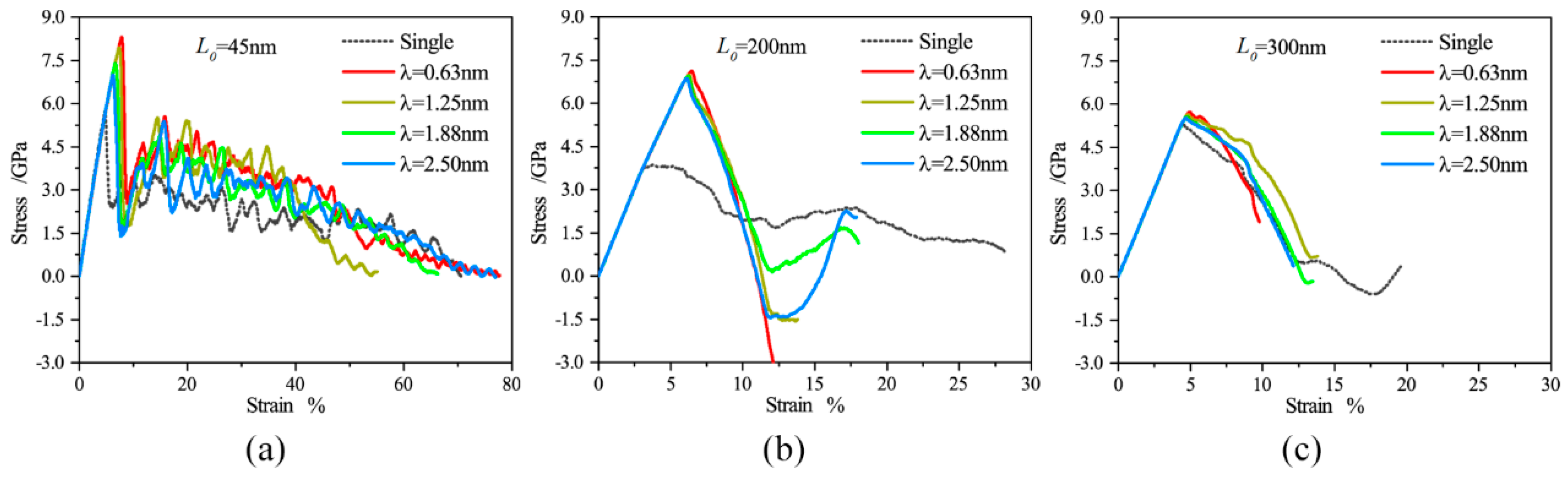
Figure 4.
Fracture map of the twinned Cu nanowires.

Figure 5.
(a) yield stress and (b) elongation to failure of twinned Cu nanowires as a function of nanowire length, showing the size-dependent mechanical properties.
Figure 5.
(a) yield stress and (b) elongation to failure of twinned Cu nanowires as a function of nanowire length, showing the size-dependent mechanical properties.

Figure 6.
(a) yield stress and (b) elongation-to-failure of the twinned Cu nanowires as a function of twin boundary spacing.
Figure 6.
(a) yield stress and (b) elongation-to-failure of the twinned Cu nanowires as a function of twin boundary spacing.

Figure 7.
Snapshot of the twinned Cu nanowires with L0 = 45 nm and λ = 1.88 nm during stretching at stain of (a) 6.40%; (b) 6.48; (c) 6.60%; (d) 6.65%. On the left panel, the atoms are colored according to the SVA. On the right panel, the atoms are colored according to the CNA, where the atoms with face-centered cubic (FCC) lattice are hid. The inserts show the magnification of the positions highlighted by the yellow rectangle box.
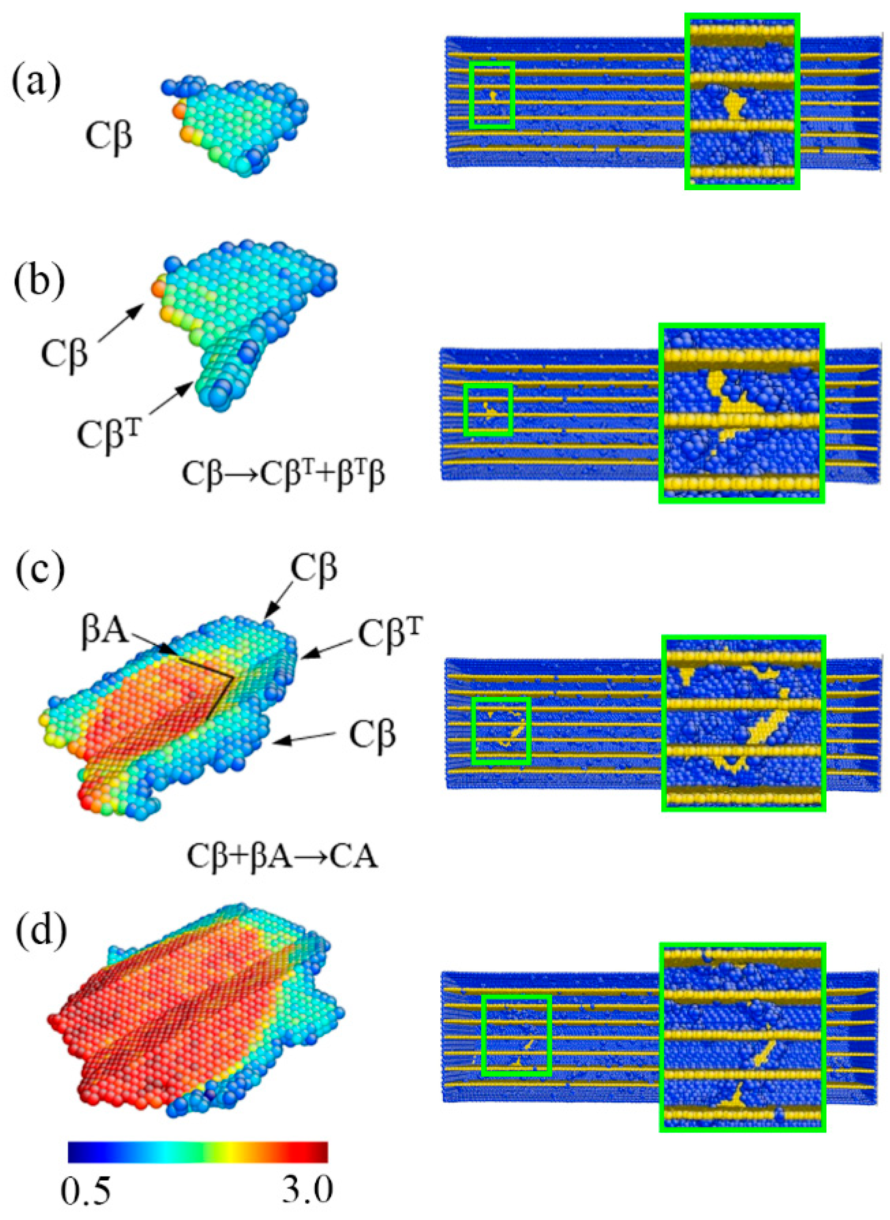
Figure 8.
The cross-section view (left panel) and full view (right panel) of atomic snapshot of the twinned Cu nanowires with L0 = 45 nm and λ = 1.88 nm during stretching at stain of (a) 7.00%; (b) 8.25%; (c) 14.90%; (d) 25.10%; (e) 49.50%. The atoms are colored according to the SVA.
Figure 8.
The cross-section view (left panel) and full view (right panel) of atomic snapshot of the twinned Cu nanowires with L0 = 45 nm and λ = 1.88 nm during stretching at stain of (a) 7.00%; (b) 8.25%; (c) 14.90%; (d) 25.10%; (e) 49.50%. The atoms are colored according to the SVA.
© 2017 by the authors. Licensee MDPI, Basel, Switzerland. This article is an open access article distributed under the terms and conditions of the Creative Commons Attribution (CC BY) license (http://creativecommons.org/licenses/by/4.0/).
Share and Cite
MDPI and ACS Style
Sun, J.; Li, C.; Han, J.; Shao, X.; Yang, X.; Liu, H.; Song, D.; Ma, A. Size Effect and Deformation Mechanism in Twinned Copper Nanowires. Metals 2017, 7, 438. https://doi.org/10.3390/met7100438
AMA Style
Sun J, Li C, Han J, Shao X, Yang X, Liu H, Song D, Ma A. Size Effect and Deformation Mechanism in Twinned Copper Nanowires. Metals. 2017; 7(10):438. https://doi.org/10.3390/met7100438
Chicago/Turabian StyleSun, Jiapeng, Cheng Li, Jing Han, Xiaoyan Shao, Xiaowei Yang, Huan Liu, Dan Song, and Aibin Ma. 2017. "Size Effect and Deformation Mechanism in Twinned Copper Nanowires" Metals 7, no. 10: 438. https://doi.org/10.3390/met7100438
Note that from the first issue of 2016, this journal uses article numbers instead of page numbers. See further details here.