Experimental Analysis on the Molten-Phase Dewetting Characteristics of AuPd Alloy Films on Topographically-Structured Substrates


Dipartimento di Fisica e Astronomia, Università di Catania and MATIS CNR-IMM, via S. Sofia 64, 95123 Catania, Italy
Metals 2017, 7(9), 327; https://doi.org/10.3390/met7090327
Submission received: 14 July 2017
/
Revised: 21 August 2017
/
Accepted: 22 August 2017
/
Published: 25 August 2017
(This article belongs to the Special Issue Metallic Films: From Nanofabrication and Nanostructuration to Characterizations and Applications)
Abstract
:AuPd nanoparticles are formed on fluorine-doped tin oxide (FTO) by a nanosecond laser irradiation-induced dewetting process of deposited AuPd films. In particular, we analyze the effect of the surface topography of the substrate on the dewetting process and, so, on the final mean size of the formed nanoparticles. In fact, we used two supporting FTO substrates differing in the surface topography: we used a FTO layer which is un-intentionally patterned since it is formed by FTO pyramids randomly distributed on the glass slide as result of the deposition process of the same FTO layer, namely substrate A. We used, also, a further FTO substrate, namely substrate B, presenting, as a result of a chemical etching process, a higher roughness and higher mean distance between nearest-neighbor pyramids with respect to substrate A. The results concerning the size of the obtained AuPd NPs by the laser irradiations with the laser fluence fixed shows that the substrate topography impacts on the dewetting process. In particular, we found that below a critical thickness of the deposited AuPd film, the NPs formed on substrates A and B have similar size and a similar trend for the evolution of their size versus the film thickness (i.e., the dewetting process is not influenced by the substrate topography since the film does not interact with the substrate topography). On the other hand, however, above a critical thickness of the deposited AuPd film, the AuPd NPs show a higher mean size (versus the film thickness) on substrate B than on substrate A, indicating that the AuPd film interacts with the substrate topography during the dewetting process. These results are quantified and discussed by the description of the substrate topography effect on the excess of chemical potential driving the dewetting process.
1. Introduction
The generation of metallic nanostructures on surfaces is a thrust in materials science from the scientific viewpoint and technological applications in areas such as catalysis, photonics, plasmonics, solar cells, single electron, and quantum devices, etc. [1,2,3,4,5,6,7,8,9,10,11,12,13,14,15,16]. For example, metal nanoparticles (NPs), such as Au and Ag, on conductive transparent substrates show interesting optical properties exhibiting structure-dependent transmission/absorption spectra due to localized surface plasmon resonances [8,9,10,11,12]. On the other hand, for example, Pd and Pt NPs on functional substrates, are particularly interesting due to their catalytic activity in several important chemical reactions on surfaces [17,18,19,20,21]. In addition, bimetallic NPs are attracting a large interest due to the possibility to largely tune their properties by the control of the relative composition, in addition to their size and shape [22,23,24]. For example, bimetallic catalysts have attracted considerable attention because their properties often differ markedly from either of the constituent metals, with the mixtures frequently exhibiting enhanced catalytic stabilities, activities, or selectivities [25,26]. In this framework, AuPd alloys are frequently used as catalysts, for example, in CO oxidation, synthesis of vinyl-acetate monomer, etc. [27,28]. Pd is an excellent catalyst for many catalytic reactions and, recently, it has been shown that its activity and selectivity can be significantly enhanced by the addition of Au. Therefore, AuPd alloy catalysts have been the subject of several investigations. In addition, bimetallic AuPd NPs have important applications in various domains, showing enhanced properties with respect to bimetallic surfaces [29]. On the other hand, chemically- and physically-synthesized AuPd NPs are attracting a great deal of interest due to the synergic effect of the two combined metals, Au being an excellent plasmonic material, and Pd an excellent catalytic material [22,23,24,29]. In addition to catalytic applications, these systems can exploit their functional properties in sensor applications [30,31,32], plasmonics [30,33], photocatalysis [34], hydrogen storage [35], etc. In general, the properties of NPs bridge those of bulk and atomic systems (size effects), and such properties are wide-range modifiable by the manipulation of the structural ones. In addition to size and shape, in bimetallic NPs, the control of the chemical composition (relative concentration of the two components) also allows further manipulation of the NPs properties.
Concerning the specific case of the AuPd alloy, this system shows no miscibility gap (above 300 K) for the whole range of concentrations, forming continuous and homogeneous solid solutions across the entire range of composition [36]. Thus, it can be seen as a model system in view of the formation of bimetallic functional NPs from a continuous and homogeneous alloy. In this framework, however, the real exploitation of bimetallic AuPd NPs in technological devices is conditioned to the development of simple, versatile, low-cost, high-throughput methods for the fabrication of the bimetallic nanoparticles, which allow the fine control of their structural properties (such as size).
Starting from these considerations, in this work we propose and analyze a method to produce AuPd NPs directly on surfaces. In particular, we deposited AuPd composite films on a transparent conductive oxide (fluorine-doped tin oxide (SnO2:F) on glass (soda-lime), i.e., FTO)/glass) and we observed that after nanosecond laser irradiations a molten-phase dewetting process of the films occurs leading to the formation of NPs on the FTO surface. FTO was chosen as a model substrate: nowadays, it is routinely used as a transparent coating for solar cell energy heat mirrors for its high electrical conductivity and high transparency at the visible and near-IR region of the electromagnetic spectrum.
Thus, after the deposition of the AuPd film with various thickness d on the FTO surface, we performed the nanosecond laser irradiations. From a general point of view, the application of ultrafast lasers for material nano-processing allows for obtaining a wide variety of nanostructures as a result of laser induced melting and solidification dynamics [37,38,39,40,41,42,43]. The main advantages of laser-based approaches include: local processing down to the micrometer and sub-micrometer range; minimized thermal damage to substrate and neighboring regions; non-contact nature and non-planar processing. The breakup of deposited metal films into NPs is observed under laser irradiation as a consequence of the films’ melting and solidification processes, known as a dewetting process of the molten metal films [39,40,41,42,43,44,45,46,47,48,49,50,51].
We studied the evolution of the mean diameter <D> of the formed AuPd NPs versus the starting thickness of the deposited AuPd film onto the FTO surface. As predicted, <D> increases with the increase of d. However, we highlight a further result: the dependence of the NPs size on the topography of the substrate. In fact, generally, the dewetting of deposited thin metal films is analyzed on flat substrates [39,40,41,42,43,44,45,46,47]. However, some works demonstrated that specific intentional patterning of substrate Affects the spatial distribution and size of the NPs formed by the dewetting process of a deposited film [48,49,50,51]. The FTO layer that we use as substrate is un-intentionally patterned since it is formed by FTO pyramids randomly distributed on the glass slide as result of the deposition process of the same FTO layer [52,53], namely substrate A. We characterized the topography of this substrate by measuring its roughness and mean distance between nearest-neighbor pyramids. Thus, in order to study the effect of the substrate topography we used a further FTO substrate, namely substrate B, presenting a higher roughness and higher mean distance between nearest-neighbor pyramids with respect to substrate A. The results concerning the size of the AuPd NPs produced by the laser irradiations when the laser fluence was fixed show that the substrate topography impacts on the dewetting process. In particular, we found that below a critical thickness of the deposited AuPd film, the NPs formed on substrates A and B have similar size and a similar trends for the evolution of their size versus the film thickness (i.e., the dewetting process is not influenced by the substrate topography since the film does not interact with it). On the other hand, however, above a critical thickness of the deposited AuPd film, the AuPd NPs show higher mean size (versus the film thickness) on substrate B than on substrate A, indicating that the AuPd film interacts with the substrate topography during the dewetting process. These results are quantified and discussed by the description of the substrate topography effect on the excess of chemical potential driving the dewetting process [48,49,50].
We point out that some previous works exploited the dewetting process of bimetallic films or of bilayers of two deposited metals to produce arrays of bimetallic NPs on surfaces [54,55,56,57,58,59,60,61,62]. In particular, in these works, bimetallic films (CoPd, CoAu, NiCu, AuPt) [54,55,59,62] or bilayers of different metals (Au/W, Au/Ag, Pt/Ni, Ag/Co, Au/Fe) [56,57,58,60,61] were deposited on flat oxide surfaces and their mixing and dewetting processes were induced exploiting standard furnace annealing at temperatures lower than the melting temperatures of the two metals (i.e., solid-state dewetting) [54,55,56,58,59,61,62] or by nanosecond laser irradiation (i.e., liquid-state dewetting) [57,60]. As a consequence, arrays of homogeneous alloy NPs were obtained if the two metals were miscible (as in the case, for example, of CoPd and Au/Ag) or arrays of heterogeneous alloy NPs were obtained if the two metals were immiscible (as in the case, for example, of CoAu and Ag/Co).
2. Materials and Methods
For the experiments presented in this work, we used two types of fluorine-doped tin oxide (SnO2:F, FTO)/glass (soda-lime) substrates differing by the surface roughness RMS (root mean square). We used an as-grown FTO layer on glass slides which we name substrate A. These slides were purchased from KINTEC (Hung Hom, Kowloon, Hong Kong) [63]. They present a 73.2% average transmittance in the 400–1100 nm radiation wavelength range [64] (and RMS = 19.4 nm). We also used an FTO layer on glass slides, which was chemically textured to enhance the surface RMS (to 32.4 nm) and we name it substrate B. This substrate was furnished by 3SUN industry (Catania, Italy). 3SUN uses this type of substrate as a transparent conductive oxide on which commercial Si-based thin film solar cells are grown [65]. The chemical etching of the FTO layer is performed to increase its surface texturing and, so, to maximize the light diffusion within the active region of the cell. Substrate B presents an 82.9% average transmittance in the 400–1100 nm radiation wavelength range [65]. Since substrate A and substrate B present different surface topographies (as we will show in the next section), they will serve to study the effect of the topography on the molten-state dewetting process of deposited AuPd films.
AuPd films (Au64Pd36 atomic %) depositions were carried out onto the FTO/glass slides (i.e., onto the FTO surface) using an RF Emitech K550X sputter coater (Quorum Technologies, East Sussex, UK), using Ar flow in the chamber at pressure of 0.02 mbar and 40 mm of target-substrate distance. Tuning the emission current and deposition time, the effective thickness d of the deposited AuPd film can be tuned. In particular, the effective thickness of the deposited films were checked ex-situ by Rutherford backscattering analysis (performed on reference samples produced by the deposition of the AuPd films on Si substrates). These analyses were performed by using 2-MeV 4He+ backscattered ions with a scattering angle of 165° and indicated the following thicknesses for the deposited AuPd films: d = 4.3 nm, 5.8 nm, 7.5 nm, 9.8 nm, 19.8 nm, 29.2 nm, 38.3 nm, and 48.6 nm. The error in the film thickness measurement is 5%.
Laser irradiation was performed by a pulsed (12 ns) Nd:yttrium aluminum garnet YAG laser operating at 532 nm (Quanta-ray PRO-Series pulsed Nd:YAG laser) (Spectra Physics, Santa Clara, CA, USA). The spot laser has a circular shape of 4 mm in diameter. The laser intensity profile is Gaussian and is characterized by a full width at half maximum of 1 mm. 97% of the highest laser intensity is maintained within a circular area of 600 μm in diameter centered at the maximum of the laser intensity. The error in the fluence measurement is 0.025 J/cm2. Concerning the laser irradiations of the samples, we performed one pulse per sample fixing the 0.50 J/cm2 fluence.
Atomic force microscopy (AFM) analyses were performed using a Bruker-Innova microscope (Bruker, Santa Barbara, CA, USA) operating in high-amplitude mode and ultra-sharpened Si tips were used (MSNL-10 from Bruker Instruments, with anisotropic geometry, radius of curvature ~2 nm, tip height ~2.5 μm, front angle ~15°, back angle ~25°, side angle 22.5°). The Si tips were substituted as soon as a resolution loss was observed during the AFM image acquisition. The AFM images were analyzed by using the SPMLABANALYSES V7.00 software (version 7.00, Bruker, Santa Barbara, CA, USA).
Scanning electron microscopy (SEM) analyses were performed using a Zeiss FEG-SEM Supra 25 Microscope (Carl Zeiss Microscopy, New York, NY, USA) operating at 5 kV. The SEM images were analyzed by Gatan Digital Micrograph software (version 3.0, GATAN Inc., Pleasanton, CA, USA). In particular, to extract the mean diameter <D> of the particles from the SEM images, several SEM images per sample were considered, each containing several particles. Then, for each image we set a threshold on the brightness of the image, so that the bright regions in the images, with intensity value 1, represent the metal particles and the dark regions, with intensity value 0, represent the supporting substrate. The diameter D of a particle is evaluated as the diameter of the smaller circle inscribing the particle. The mean value <D> of the particles for each sample has been calculated on a statistical population of 200 particles per sample, with the error the standard deviation on the mean value.
3. Results and Discussion
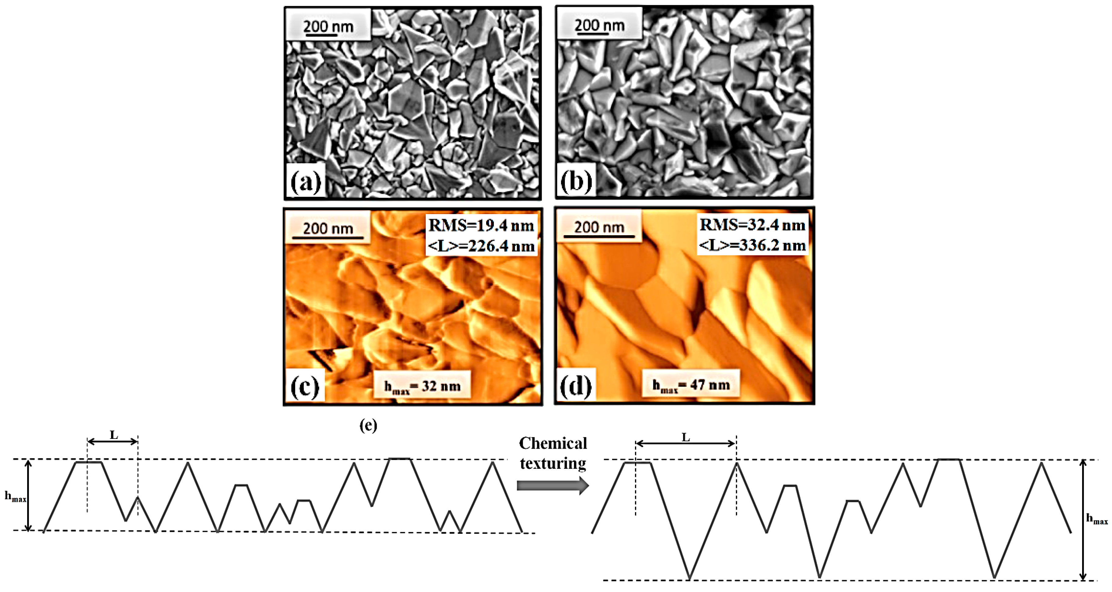
Firstly, we proceeded to the morphological analysis of the bare FTO/glass substrates (substrate A and B) which we then used as supporting substrates for the following AuPd films depositions. Thus, we performed SEM and AFM analysis to study the surface morphological characteristics of the FTO layers. Figure 1 shows representative SEM images of the FTO namely substrate A ((a), FTO on glass as purchased), and of the FTO namely substrate B ((b), FTO chemically textured on glass).
As evident, the FTO layers are formed by structures that, by the plan-view images, remember pyramids which are randomly distributed on the glass slide. This morphology is typical as a result of the deposition process of the FTO layer [52,53]. Similarly, Figure 1 shows representative AFM images of substrate A ((c), FTO on glass as purchased), and of substrate B ((d), FTO chemically textured on glass). In particular, the AFM analysis allowed to extract the surface roughness of the FTO surface for substrate A and B. The surface roughness is quantified by the RMS parameter. It is defined by RMS = <z(x, y)2>1/2 being z(x, y) = h(x, y)-<h(x, y)> with h(x, y) being the height function and <…> being the spatial average over a planar reference surface [66,67]. We found RMS = 19.4 nm for substrate A and RMS = 32.4 nm for substrate B, indicating a higher surface roughness for substrate B. This is in agreement with the fact the FTO layer in substrate B, differently from the FTO layer in substrate A, was chemically textured in view of its standard application as transparent and conductive component for thin-film Si-based solar devices (the texturing enhance the forward incident scattered radiation). In addition, we used the plan-view SEM images to estimate the mean top-to-top distance <L> between the nearest neighbour pyramids forming the FTO layer. We obtained <L> = 226.4 nm for substrate A (non-textured FTO layer) and <L> = 336.2 nm for substrate B (textured FTO layer). Thus, on the basis of the RMS and <L> values we can sketch the representative cross-line profile for the FTO layer in the substrates A and B in order to highlight the main morphological differences: Figure 1e presents these pictorial representations, substrate A on the left and substrate B on the right. According to the different values of RMS and <L>, these representation summarizes the fact that: (i) the chemical etching process of the FTO layer leads to an increase of the mean bottom-to-top distance between the base and the apex of the pyramids (i.e., height of the pyramids), as indicated by the increase of the RMS value. Additionally, the maximum height (the distance from the lower point and the higher point measured by the AFM tip) recognized by the AFM measurement increases from 32 nm in the sample A to 47 nm in the sample B; (ii) the chemical etching process of the FTO layer leads to an increase of the mean top-to-top distance between the nearest neighbour pyramids forming the FTO layer. We can conclude, therefore, that sample A and B, even if they are formed by an FTO layer deposited on glass, present different surface topographies.
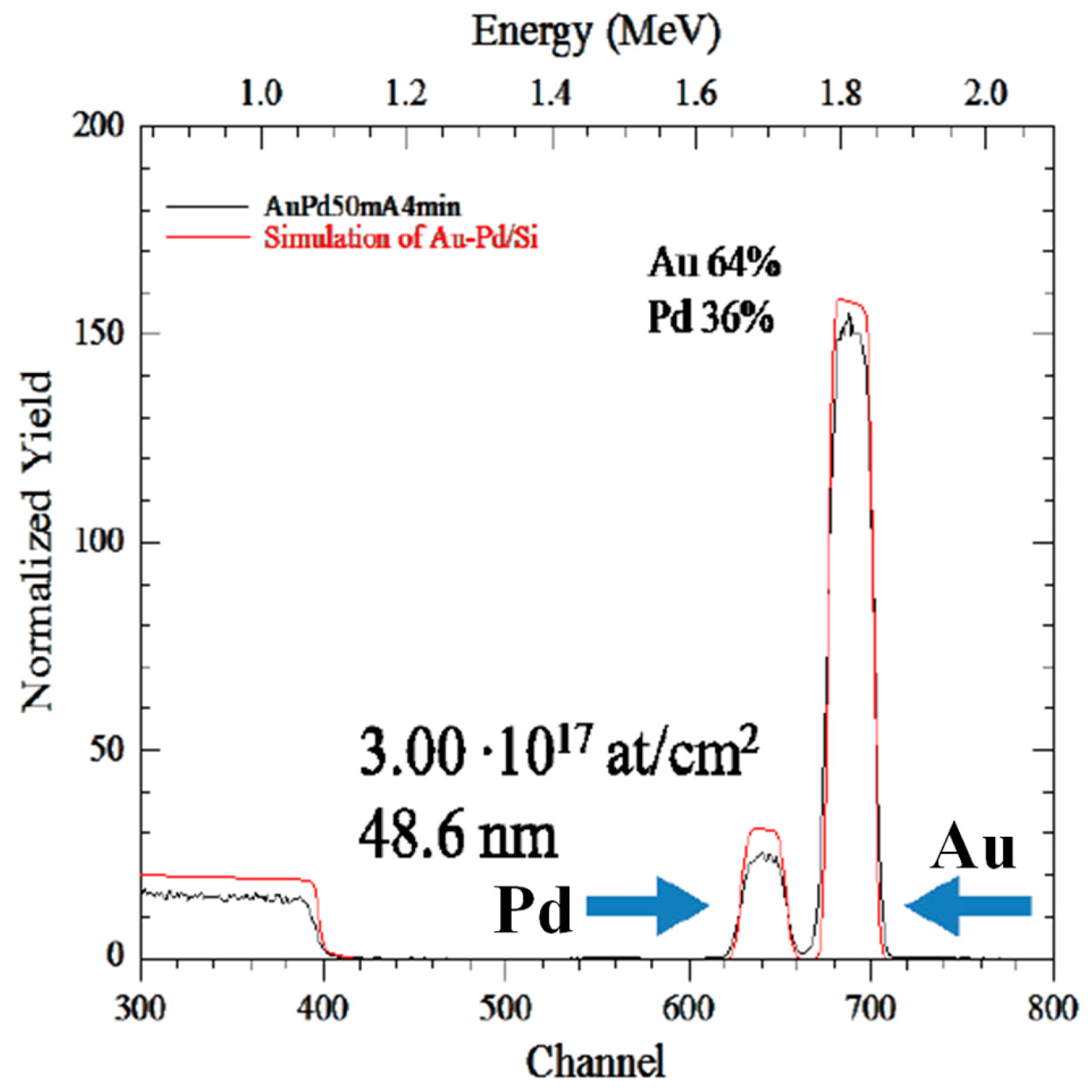
Then we proceeded to the AuPd depositions. The thickness of the deposited AuPd films were calibrated by depositing them on Si slides and by performing ex situ Rutherford Backscattering Spectrometry (RBS) analysis. Thus, we chose to deposit AuPd films of effective thicknesses d = 4.3 nm, 5.8 nm, 7.5 nm, 9.8 nm, 19.8 nm, 29.2 nm, 38.3 nm, 48.6 nm on substrates A and B. The RBS analysis confirmed, also, the Au64Pd36 atomic % composition of the films. For example, Figure 2 reports the experimental RBS spectrum (black line) for the AuPd film deposited on a Si slide (to easily proceed to the RBS analysis) and the corresponding simulation (red line) from which the total thickness of 48.6 nm for the film is derived so as the Au64Pd36 atomic % composition. In the spectrum, the two peaks corresponding to the presence of Au and Pd are clearly recognizable.
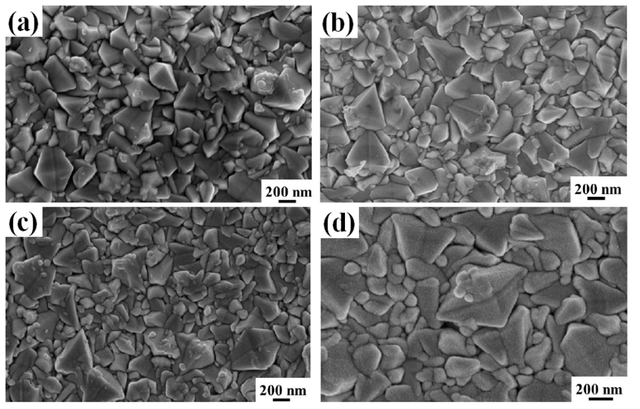
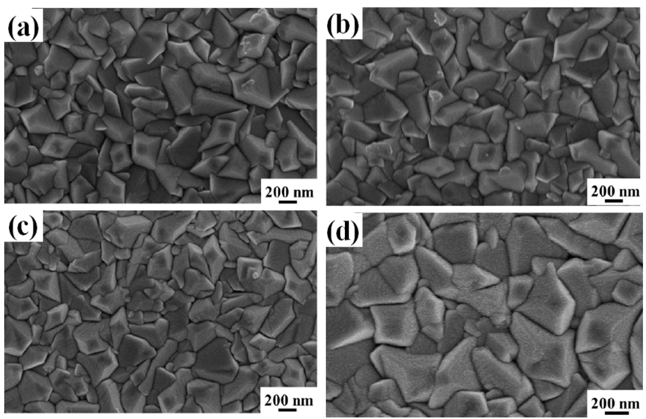
Then we proceeded to perform a surface morphological inspection of the as-deposited AuPd films by SEM analysis. As examples, Figure 3 reports representative SEM images of the surface of the FTO layer in substrate A after deposition of the AuPd film with d = 4.3 nm (a), d = 7.5 nm (b), d = 29.2 nm (c), and d = 48.6 nm (d). Similarly, Figure 4 reports representative SEM images of the surface of the FTO layer in substrate B after deposition of the AuPd film with d = 4.3 nm (a), d = 7.5 nm (b), d = 29.2 nm (c), and d = 48.6 nm (d). The increase in the amount of deposited AuPd can be recognized in the appearence of a nano-granular morphology over the FTO pyramids: this is typical for a Volmer-Weber growth mode of metal films on non-metal substrate [6,42,43,47,68]. In this case, at the early stages of growth, metal particles may grow on the surface through homogeneous nucleation (i.e., island formation due to nucleation on defect-free terraces) and heterogeneous nucleation (island formation at steps and other defects) [68].
In order for islands to form on the substrate, atoms deposited from the vapor phase undergo a series of kinetic processes, including thermal accommodation onto the substrate, surface diffusion of the adatoms on the surface, dimer formation to initiate nucleation, then island formation and growth. As more and more atoms are deposited, small islands may grow, contact each other, and then fully coalesce (i.e., two islands merge) into larger, but still compact, three-dimensional nano-islands, which are those recognizable in Figure 3d and Figure 4d.
Then, we proceeded to the laser irradiations (1 pulse, 0.50 J/cm2) and to the SEM analysis to study the effect of the irradiations on the AuPd films. In general, after exposure to 0.50 J/cm2 laser irradiation the film is observed to melt and broken up into NPs of circular sections (see Figure 5).
The characteristics of the molten-phase dewetting process [39,40,41,42,43,44,45] can be inferred by Figure 5 where we report, as an example, the plan-view SEM images of the AuPd bilayer irradiated by 0.5 J/cm2 and acquired at different distances from the center of the spot. In particular, Figure 5a shows an optical photo reporting an example of the laser spot as obtained by irradiating the 29.2 nm-thick AuPd film deposited on the textured FTO (substrate B). As pictured in Figure 5b, roughly three anular regions can be identified close to the center of the spot and corresponding to an increase of the laser fluence from region 1 to region 3, whereas the maximum laser fluence of 0.5 J/cm2 is obtained in region 3. Thus, Figure 5c–e reports representative SEM images of the sample surface acquired in region 1 ((c), at a distance >600 µm from the spot center), region 2 ((d), at a distance between 300 μm and 600 µm from the spot center), and region 3 ((e), at a distance lower than 300 µm from the spot center): this sequence of images clearly shows the dewetting process of the AuPd film. Figure 5c shows that in region 1, the film perforate and the molten film around these perforations is observed to have drawn away from the center of the hole. These perforations occur at thickness inhomogeneities in the film, as the fluence required for melting is lower for thinner films [41]. However, the dewetting process is, only in the initial phase evolution: the break-up into discrete droplets was incomplete. The forming holes in the film leave an exposed FTO surface and some NPs in these holes (see Figure 6 for a higher magnification image). The other zones of the film are unaltered by the laser irradiation. In region 2 of the spot (Figure 5d), where the fluence is higher, the density of perforations is increased so that the retreating molten film between two holes can coalesce into filaments. Some of these filaments are clearly visible and they extend from the unaltered regions to the holes. These filaments, or liquid metal nanowires, can then split into droplets due to the Rayleigh instability [41,42]. Finally, in region 3, where the laser fluence is maximum (0.5 J/cm2), the dewetting process is complete: all the filaments were decomposed in NPs resulting with the formation of an array of NPs distributed over the entire region within a radius of about 300 µm from the center of the laser spot.
In metals such as Au and Pd, the equilibrium between hot electrons and the lattice takes place with a time limit of up to t* = 50 ps [39,40,41,42,43,44,45]. However, in the present experiments, the pulse time is τ = 12 ns >> t* so that in our experiments the AuPd melt dynamics is the dominant process, as is typical for such metals under nanosecond laser irradiation [39,40,41,42,43,44,45]. The observed dewetting process occurs, therefore, with the AuPd alloy films in the molten state.
Regarding the following quantitative analyses, the relevant parameters are extracted by considering, for each sample, the NPs formed within a region of radius of 300 µm from the center of the laser spot so that we are sure to analyze and compare NPs formed all at the same laser fluence of 0.5 J/cm2. These SEM studies are summarized in Figure 7, Figure 8 and Figure 9: as examples, Figure 7 reports representative SEM images, of the NPs formed by irradiating the AuPd film with thickness 4.3 nm (a), 7.5 nm (b), 29.2 nm (c), 48.6 nm (d) deposited on the untreated FTO substrate (substrate A); similarly, Figure 8 reports SEM images of the NPs formed by irradiating the AuPd film with thickness 4.3 nm (a), 7.5 nm (b), 29.2 nm (c), and 48.6 nm (d) deposited on the textured FTO substrate (substrate B); finally, Figure 9 reports enlarged SEM images of the NPs formed by irradiating the AuPd film with thickness 9.8 nm ((a) and (d)), 19.8 nm ((b) and (e)), 48.6 nm ((c) and (f)) deposited on the untreated FTO ((a), (b), and (c)) and on the textured FTO ((d), (e), and (f)).
From a quantitative point of view, the SEM images were analyzed to extract the distributions of the NP diameter D, as described in the experimental section. Using these distributions, each sample the mean diameter <D> (and the corresponding standard deviation ΔD) of the NPs produced by the 0.5 J/cm2 laser irradiation can be evaluated.
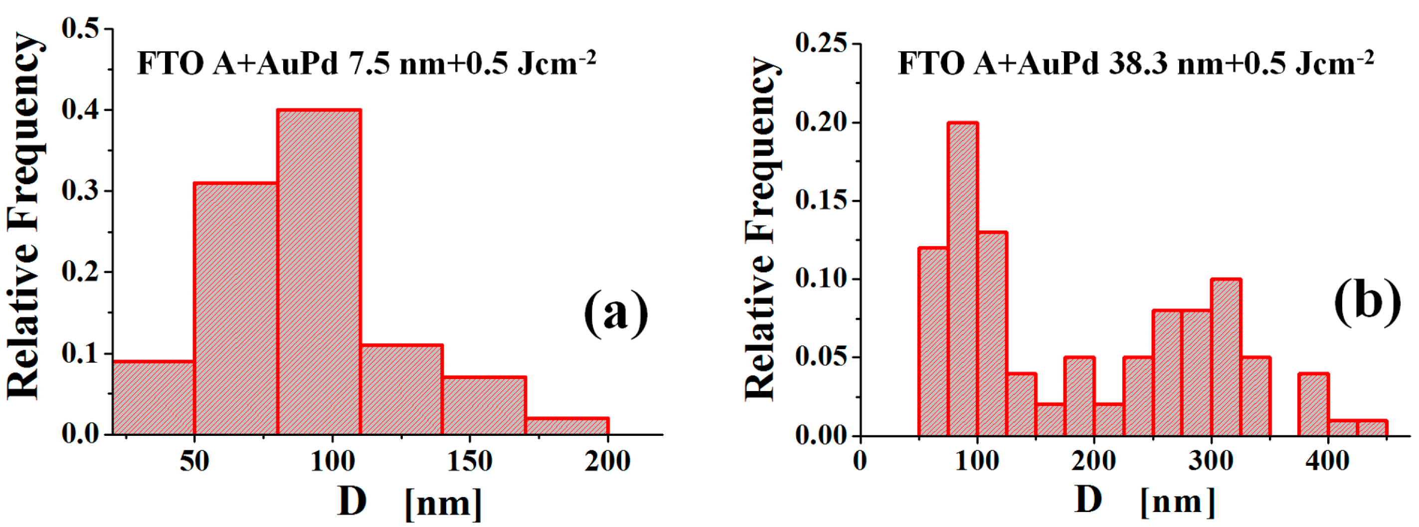
Extracting these distributions, we noted that the distributions corresponding to NPs obtained from the irradiations of the AuPd films with tichkness d = 38.3 nm and d = 48.6 nm (the highest ones) were bimodal distributions (two peaks in the distributions) whereas the distributions corresponding to the NPs obtained from the irradiations of the AuPd films of lower thickness resulted in monomodal distributions (one peak in the distributions). The appearing of a double-sized distribution for the NPs is, for example, evident from observing Figure 9c,f. Quantitatively, Figure 10 reports some examples of the extracted distributions: (a) shows the distribution of diameters D for the NPs obtained, on substrate FTO A, by the laser irradiation of the 7.5 nm-thick AuPd film, while (b) shows the distribution of diameters D for the NPs obtained, on substrate FTO A, by the laser irradiation of the 38.3 nm-thick AuPd film. The difference between these size distributions is clearly evident: in (a) all the NPs belong to an unique population characterized by an unique peak in the distribution; in (b) the NPs belong to two different subpopulations each with a proper peak in the distribution. The reason for this evolution of the NPs size distribution when increasing the film thickness is, reasonably, the following [69,70]: until a critical metal film thickness (which is material-dependent) the temperature of a metal film irradiated by the nanosecond laser increases when the film thickness increases [71]. Thus, at a high enough thickness, the metal film can reach a temperature higher than the metal boiling temperature.
The consequence is photo-fragmentation of the NPs, which are formed by the dewetting process [69,70]. This fragmentation can occur, for example, but not only, by metal atoms which evaporate from large formed metal clusters. These evaporate atoms re-condensate on the substrate surface forming smaller clusters. The final result is the formation of larger NPs surrounded by smaller NPs, i.e., the two NPs subpopulations observed by us for the arrays originated from the irradiations of the 38.3 nm and 48.6 nm thick AuPd films. However, for all the samples, independently on the starting thickness of the deposited film, we calculated the mean diameter <D> of the obtained NPs on the entire population constituting the NPs arrays. Figure 11 summarizes the results of these quantitative analysis: (a) reports, in log-log plot, the NPs mean diameter <D> versus the starting thickness d of the deposited AuPd film on the untreated FTO substrate (substrate A); similarly, (b) reports, in log-log plot, the NPs mean diameter <D> versus the starting thickness d of the deposited AuPd film on the textured FTO substrate (substrate B).
The comparison of these plots clearly indicate an effect of the substrate topography on the dewetting process, i.e., in the resulting <D>. In particular the following conclusions and discussions can be drawn:
(a) A critical thickness d = dc can be identified from the plots in Figure 11. It is 9.8 nm < dc < 19.8 nm. Roughly, below dc the experimental points <D> versus d follow a specific behavior (a straight line in the log-log plot), while above d’ the experimental points follow a different behavior (in the log-log plot, a straight line with decreased rate). This occurs both on substrates A and B. Thus, fixing the substrate, the critical thickness dc identifies a change in the dewetting characteristics of the AuPd film.
(b) Below the critical thickness dc, the NPs obtained on substrates A and B present very similar values of <D> for each fixed d. On the contrary, above d’, the mean diameter <D> is higher, at each fixed d, for the NPs obtained on substrate B (textured FTO) than for the NPs obtained on substrate A (untreated FTO). Thus, we have to conclude that below dc the substrate topography does not influence the AuPd film dewetting process, while above dc the topography of the substrate is crucial in determining the dewetting process and, so, the final mean size of the produced NPs. As evident, the effect of the substrate topography on the film dewetting is, therefore, conditioned to the thickness of the deposited film. Figure 12 and Figure 13 schematically visualize the effect of the dewetting process of the AuPd film for d < dc and d > dc on the untreated FTO (Figure 12) and on the textured FTO (Figure 13): dc could be thought to be related to some characteristic size of the features of the substrate (pyramids height or aspect ratio, i.e., pyramid height/pyramid planar size, etc.). Thus, when d < dc, the geometrical (i.e., topographic) features of the substrate do not influence the dewetting of the films (Figure 12a and Figure 13a). In other words, the film does not interact with the topographic features of the substrate since the substrate acts as a planar substrate for the film. As a result, the film dewets as on a planar substrate forming NPs uniformly dispersed over the entire surface of substrate and the size of the obtained NPs, being very low with respect to the size of the characteristic size of the features of the substrate, is not influenced by the substrate topography. Instead, when d > dc the geometrical (i.e., topographic) features of the substrate influence the dewetting of the films (Figure 12b and Figure 13b). In other words, the film interacts with the topographic features of the substrate since the substrate does not act as a planar substrate for the film. As a result, the film dewetting is driven, in addition to the surface energy minimization, in some way by the topography of the substrate, leading to a preferential formation of the NPs in-between, or over, the pyramids. It is evident that some characteristic size of the pyramids influences the final NPs mean size: we can observe from Figure 11 that, for each d > dc, we obtain larger NPs on the substrate where the mean distance <L> between neighboring pyramids is larger.
This qualitative discussion finds its quantitative explanation in the specific effect of the substrate topography on the film dewetting process as discussed, for example, firstly by Gierman and Thompson [48]. In their pioneering work, the authors studied the dewetting characteristics of Au film on intentionally-patterned SiO2 substrates. In particular, the authors used a litography approach to pattern the SiO2 substrate in arrays of inverted pyramid-shaped pits. However, even if the all the substrates were patterned in these inverted pyramid shaped pits, the topography was changed by changing the characteristic sizes of the pattern features: so, substrates in which the spatial period of the pits and the pit-to-mesa width ratio is different, were fabricated. Patterns with spatial periods of the pits of 377 nm and 175 nm were produced. For each of these spatial periods, in addition, patterns with the pit-to-mesa width ratios of 1.5, 1.9, and 5.3 were produced. In our case, this is similar to the change of the maximum height hmax and mean distance <L> between neighboring pyramids in the untreated and textured FTO substrates which we used. Then, Gierman and Thompson deposited Au films (16 nm, 21nm, and 32 nm in thickness) on these patterned substrate and induced the films’ dewetting by an 800 °C annealing process. On the basis of the combination of the specific topography of the substrate (i.e., the spatial period of the pits and pit-to-mesa width ratio) and Au film thickness, the authors observed or the preferential formation of one Au NP per pit with no NPs on the mesa, or the formation of one NP per pit with some other NPs on the mesa, or the formation of multiple NPs per pit with some other NPs on the mesa, or the formation of large NPs on the mesa (often covering the pits) with no NPs in the pits. These different behaviors arise from the effect of the topography on the dewetting process of the film.
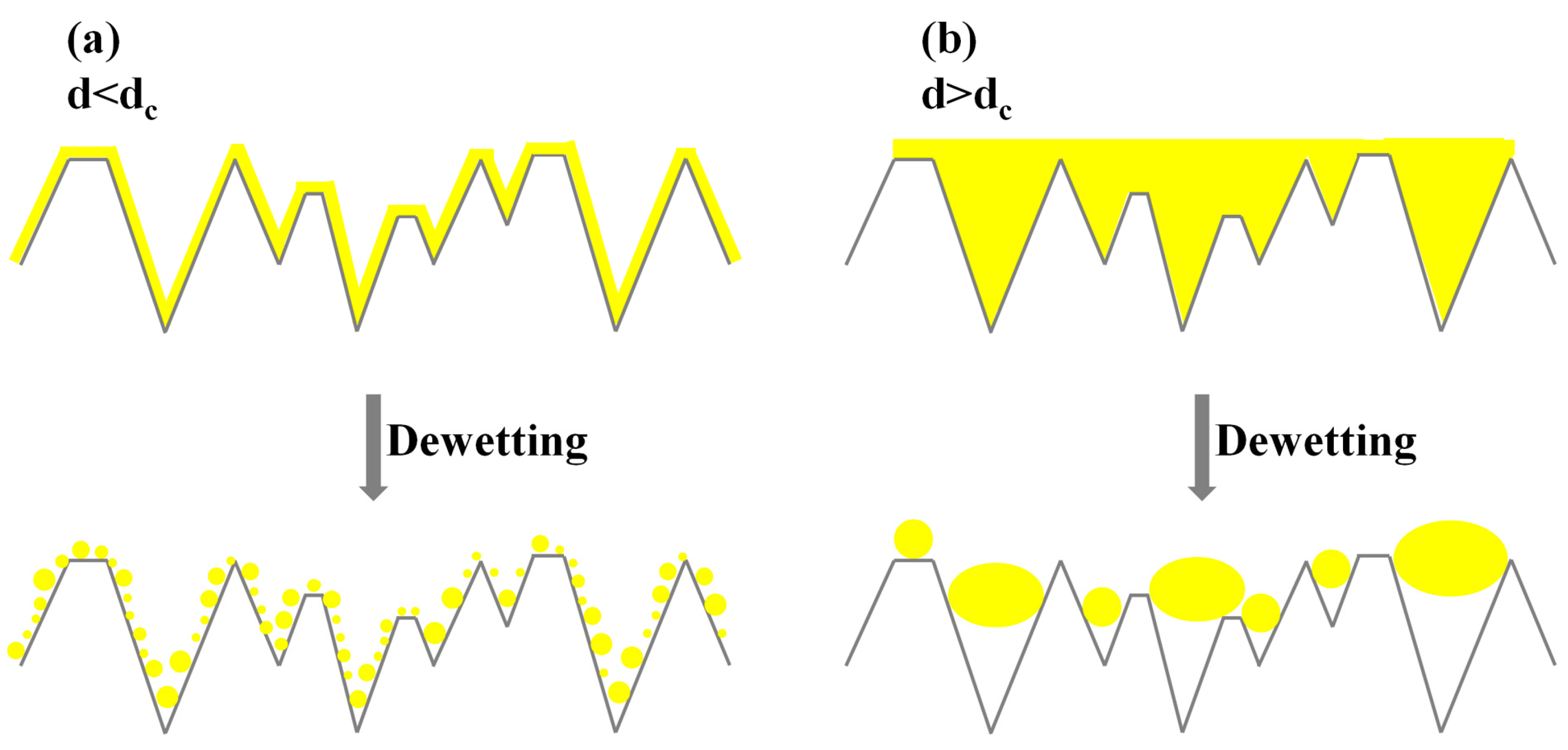
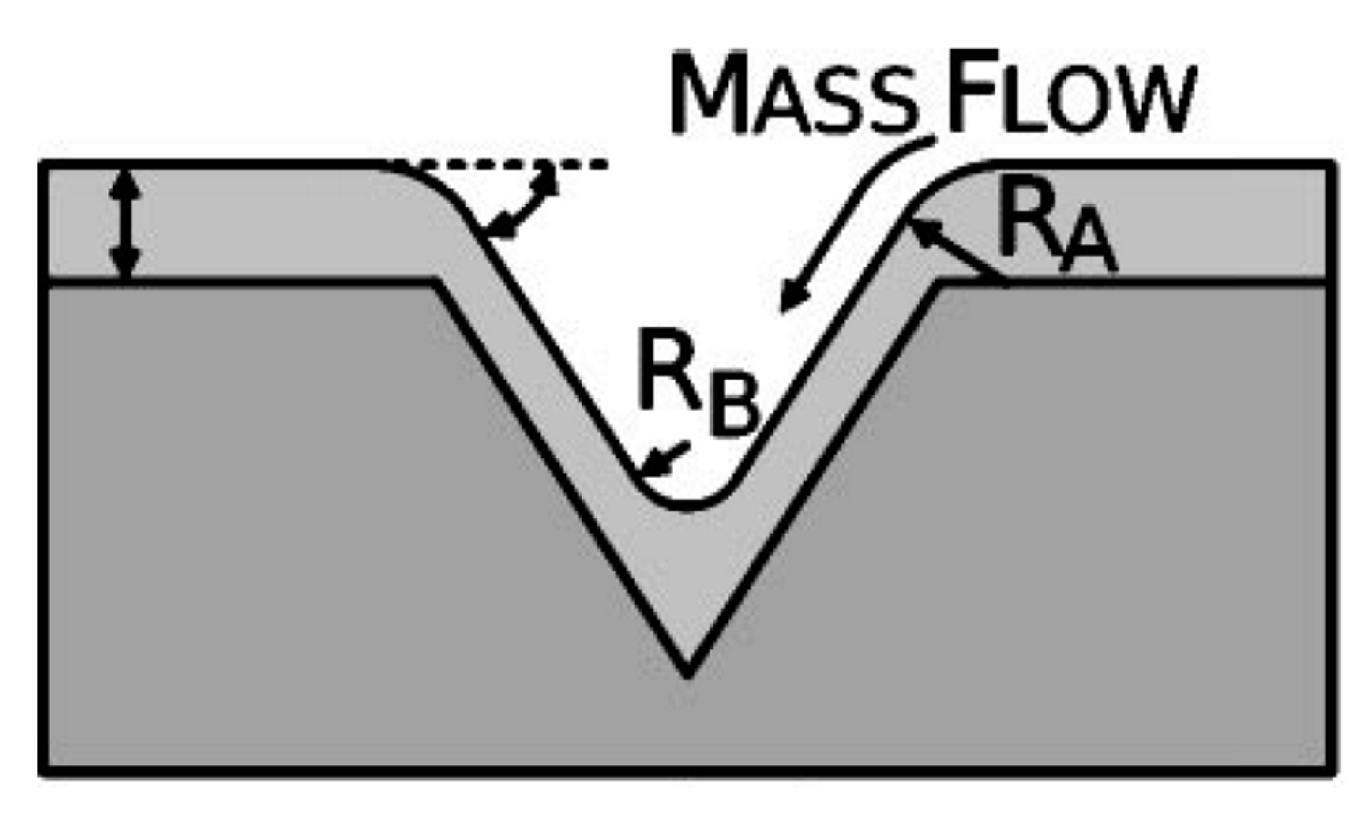
Following Giermann and Thompson, this effect can be described as follows: on a flat substrate, the dewetting process is purely driven by the minimization of the total energy of the system associated to the surfaces and interfaces. In this case, in each point of the substrate, the local curvature has no effect on the dewetting process of a deposited film. On the contrary, an excess of local chemical potential can be introduced by realizing finite local curvatures on the substrate, i.e., by pre-patterning the substrate. In fact, according to the Gibbs-Thomson relation, Δµ = κγΩ, the local excess chemical potential Δµ is dependent, in addition to the surface energy γ and atomic volume Ω of the film, on the local curvature κ where κ = 1/R with R the local radius of curvature.
For a flat substrate R → ∞ so that Δµ → 0 and, therefore, the surface topography has no effect on the film dewetting. Instead, in the case of finite R, the surface curvatures of substrate structures are associated with the chemical potential, introducing an additional driving force for the diffusion from the position with positive local curvature (peaks or ridges) to the position with negative local curvature (valleys) [50]. The result is that the surface curvature of the substrate drives the film material diffusion through modulation of the chemical potential by the substrate local curvature. For example, in the case reported by Giermann and Thompson [48], for which the substrate is patterned in inverted pyramids (see Figure 14), there will be a positive excess chemical potential at the edge of the pit proportional to κA = 1/RA and a negative excess chemical potential at the inverted apex proportional to κB = −1/|RB|. Thus, during the dewetting process, atoms of the film will diffuse away from the pit edge toward the pit apex in order to reduce the local excess chemical potentials by increasing the radius of curvature at these points. However, since the local curvature at the pit edge and the apex decreases with increasing film thickness, the driving force for flow from the edge to the apex also decreases with increasing film thickness. Thus, overall, the effect becomes dependent on the film thickness.
In synthesis, we can, at least qualitatively, describe the present experimental data on the basis of the previous considerations. Naming R the representative radius of curvature determined by the pyramidal structuration of the FTO surface, if d << R then the film dewets on the FTO substrates as supported on a flat substrate (Δµ ≈ 0, the substrate topography has no effect on the film dewetting). The resulting NPs are uniformly dispersed over the substrate surface and their mean diameter increases when the thickness of the deposited film is increased, as expected for NPs formed by dewetting of films deposited on flat substrates [46]. Increasing the film thickness d, a critical thickness dc is reached for which dc ≈ R. Thus, for film thicknesses d ≥ dc ≈ R, the surface topography influences the film dewetting by the local excess chemical potential Δµ. This is reflected, both on substrate A and B, in the change of the dependence of the mean diameter <D> of the formed NPs versus the starting thickness d of the deposited film, see Figure 11: at d < dc the experimental <D> follow the same behavior, at d > dc the experimental <D> follows the same behavior which is different from that followed at d < dc. However, it is interesting to note that, while the values of <D> for each fixed d < dc are substantially identical for the NPs formed on both substrates, at d > dc larger NPs are obtained on substrate B (the textured FTO): (<D>textured_FTO) > (<D>untreated_FTO). This is, also, coherent with the results and description by Giermann and Thompson [48]: in fact, in the condition for which the film and substrate interact by the substrate topography during the dewetting process and due to the topography-driven dewetting, the NPs are formed in the pits (in the valleys between neighboring pyramids in our case), the size of the NPs is dictated by the size of the pits (the distance between neighboring pyramids in our case). For our FTO substrates we obtained larger <L> (mean value of the distance between neighboring pyramids) for the textured FTO: so, the condition (<L>textured_FTO) > (<L>untreated_FTO) determines the (<D>textured_FTO) > (<D>untreated_FTO) result.
Two last points remain to be discussed for the sake of completeness:
(1) The linear dependence of the mean size <D> of the formed NPs versus the starting film thickness d of the deposited film. In general, the experimental analysis of the dewetting process of a metal film on a flat substrate leads to the conclusion that the size of the formed NPs increases when the film thickness increases [46]. In a general dewetting phenomenon, a thin film breaks up into particles via one of three mechanisms [46]: (1) heterogeneous nucleation (it is catalysed by a defect at the film surface or at the film-substrate interface); (2) homogeneous nucleation (caused by a thermal density fluctuation acting as a nucleus for hole formation); (3) spinodal dewetting (determined by the enhancement of periodical film thickness fluctuation). In general, however, the steps involved in a dewetting process of a film on the surface can be summarized as follows [46,47]: dewetting starts by the nucleation of holes in the film which reach the substrate surface. The holes grow with time and due to the mass-conservation and to a local curvature gradient at their edges, they develop a thickened rim. The rim increase its thickness with time so that its net curvature is reduced and edge retraction velocity reduces. The corners of the hole growing become thermodynamically unstable. Then, the rims break by a fingering instability with the consequent formation of material lines that subsequently decay into droplets through a Rayleigh-like instability [4,41,42,43,45,46]. The steady-state calculations [46,49] show that the film thickness dependence of the holes’ nucleation rate leads to a mean size <D> of the NPs which depends on the film thickness d by a power-law: <D> ∝ dα which the value of the characteristic exponent α determined by the dominant mass transport mechanism involved in the dewetting process. For example, the case of the spinodal dewetting can be exactly treated within the linear thin film hydrodynamic theory leading to α = 5/3 [41,46,49]. However, all these calculations are performed for a single component film and neglect the effect of the substrate on the dewetting process: they suppose flat surfaces and non-interacting films-substrates. In the present case of structured FTO surfaces, it is evident that the holes nucleation rate of the AuPd film during the dewetting process for d > dc must be influenced by the substrate topography by the excess of chemical potential Δµ. In our picture, however, we should expect, ideally, that for d < dc the substrate surface topography does not influence the film dewetting and, so, <D> ∝ dα. Experimentally, we obtain for d < dc, <D> = β1d, and for d > dc, <D> = β2d whereas the effect of the substrate topography is exhibited in β1 > β2 while α = 1 in both cases. We can obviously speculate that for d > dc the value of α is established, in addition, to the dominant mass transport mechanism, by the effect of the excess of chemical potential Δµ. For d < dc, in the hypothesis of a pure spinodal dewetting we should expect α = 5/3, so that the obtained value of α = 1 indicates the occurring of non-linear phenomena which could be associated to the Au and Pd interaction during dewetting or the occurring of further important mass transport mechanisms in addition to those related to a pure spinodal dewetting. This point requires further future specific theoretical calculations employing the effect of Δµ and of the Au-Pd interaction on the holes’ nucleation rate.
(2) The composition of the formed NPs. In general, the composition of bimetallic NPs formed by the dewetting process of bimetallic deposited films or bilayers of two metal films deposited on a substrate, is strictly dependent on the miscibility of the two metals [54,55]. A miscible system is a system where the constituent materials are mutually soluble in each other due to similar crystal structure, atomic radii, electronegativity, and valence. This is the case, for example, of AuPd, AuAg, CoPd, CoPt, AuPt, CoFe, AgCo, etc. In this case of miscible metals the obtained NPs are expected to be homogeneous alloy NPs [54,55,60], which is the expectation for the AuPd NPs produced in the present work. On the other hand, however, theoretical modeling studies have shown that nanomaterials may inherit a rich variety of compositional structures within the nanoparticles if the starting metals are immiscible [60], as in the case of NiAg, NiAu, AuFe, etc. In these cases, heterogeneous alloy NPs are, in general, expected by the dewetting process [54,55]. Both in the cases of miscible and immiscible metals, however, the specific amount of one metal with respect to the other has a great influences on the dewetting process by the effect on the holes’ nucleation rate. For example, in the AuPt system, the increase of the Pt content leads to a delay in the dewetting process at 500 °C [55]. This has consequences, also, on the morphology of the obtained NPs: in addition to spherical NPs, often polyhedral NPs can be obtained on the basis of the ratio amount of the two metals in the system. This is another point to be considered in the further future theoretical analyses to understand the dependence of <D> versus d that was observed in the present work. Thus, future experimental analysis on the AuPd NPs produced in the present work are needed to clarify, in detail, the structure and composition of the NPs. In this sense we will plan X-ray diffraction analysis, energy dispersive X-ray analysis, and X-ray photoelectron spectroscopy analysis to clarify this aspect. It will be interesting to analyze the composition and structure of the NPs by changing the atomic % of one of the two metals in the starting deposited AuPd film. In principle, we expect that the AuPd NPs, in particular, are homogeneous NPs with no segregation of one metal with respect to the other (i.e., we do not expect core-shell AuPd NPs), due to the AuPd miscibility. Despite this miscibility, for very small NPs (some nm in diameter) a segregation of the Pd atoms on the NPs surface is expected since Au is characterized by a slightly lower heat of sublimation and surface tension than Pd [72,73]. However, this should not be the case of the NPs produced in the present work, presenting mean diameters from about 50 nm to about 350 nm.
4. Conclusions
AuPd alloy NPs were produced on FTO substrate by inducing the molten-state dewetting process of a deposited alloy film. The AuPd films were deposited on two topographically different FTO surfaces: the first substrate is an untreated glass/FTO sample upon which the FTO is formed by microscopic pyramids presenting a mean value for the distance between neighboring pyramids of <L> = 226.4 nm, maximum height of hmax = 32 nm, and RMS = 19.4 nm; the second substrate is a glass/FTO sample upon which the FTO layer is chemically textured so that it results in being formed by microscopic pyramids presenting a mean value for the distance between neighboring pyramids of <L> = 336.2 nm, maximum height of hmax = 47 nm, and RMS = 32.4 nm. The molten-phase dewetting of the deposited films was induced by nanosecond laser irradiations at 0.5 J/cm2. The result is the formation of AuPd alloy NPs over the FTO surfaces. However, analyzing the mean diameter <D> of the formed NPs versus the thickness d of the deposited AuPd films, an effect of the substrate topography was found:
(a) Firstly, we considered that a structured substrate influences the dewetting process of a deposited film by the local surface curvature. This effect is absent when the film dewets on the flat substrate. This effect is taken into in account by considering that the local excess chemical potential Δµ is proportional to 1/R with R the local radius of curvature. In the case of finite R, the surface curvatures of substrate structures are associated with the chemical potential, introducing an additional driving force for diffusion from the position with positive local curvature (peaks or ridges) to the position with negative local curvature (valleys). Thus, as demonstrated by the experimental data <D> versus d, for the NPs produced on both substrates, a critical thickness dc of the deposited AuPd film exists: at d < dc the substrate topography does not influence the dewetting process (in fact on both substrates NPs with the same diameter are obtained). Instead, at d > dc the dewetting process is influenced by the substrate topography so that NPs with different mean diameters are obtained on the basis of the substrate.
(b) In particular, at d > dc, NPs with higher mean diameters are obtained on the textured substrate. Since the substrate topography drives the NPs formation in between the pyramids forming the FTO, and since the mean distance between neighboring pyramids is higher on the textured FTO substrate than on the untreated FTO substrate, this result on the NPs diameter arises as a consequence of this difference in the topography of the substrates.
Conflicts of Interest
The author declares no conflict of interest.
References
- Feldheim, D.L.; Foss, C.A. Metal Nanoparticles: Synthesis, Characterization, and Applications; Marcel Dekker Inc.: New York, NY, USA, 2002. [Google Scholar]
- Johnston, R.L.; Wilcoxon, J.P. Metal Nanoparticles and Nanoalloys; Elsevier: Amsterdam, The Netherlands, 2012. [Google Scholar]
- Ruffino, F.; De Bastiani, R.; Grimaldi, M.G.; Bongiorno, C.; Giannazzo, F.; Roccaforte, F.; Spinella, C.; Raineri, V. Self-organization of Au nanoclusters on the SiO2 surface induced by 200 keV-Ar+ irradiation. Nucl. Instr. Meth. Phys. Res. B 2007, 257, 810–814. [Google Scholar] [CrossRef]
- Ruffino, F.; Grimaldi, M.G. Self-organized patterned arrays of Au and Ag nanoparticles by thickness-dependent dewetting of template-confined films. J. Mater. Sci. 2014, 49, 5714–5729. [Google Scholar] [CrossRef]
- Ruffino, F.; Crupi, I.; Irrera, A.; Grimaldi, M.G. Pd/Au/SiC nanostructured diodes for nanoelectronics: Room temperature electrical properties. IEEE Trans. Nanotechnol. 2010, 9, 414–421. [Google Scholar] [CrossRef]
- Ruffino, F.; Torrisi, V.; Marletta, G.; Grimaldi, M.G. Effects of the embedding kinetics on the surface nano-morphology of nano-grained Au and Ag films on PS and PMMA layers annealed above the glass transition temperature. Appl. Phys. A 2012, 107, 669–683. [Google Scholar] [CrossRef]
- Torrisi, V.; Ruffino, F.; Licciardello, A.; Grimaldi, M.G.; Marletta, G. Memory effects in annealed hybrid gold nanoparticles/block copolymers bilayers. Nanoscale Res. Lett. 2011, 6, 167. [Google Scholar] [CrossRef] [PubMed]
- Ruffino, F.; Torrisi, V.; Marletta, G.; Grimaldi, M.G. Patterning of templated-confined nanoscale Au films by thermal-induced dewetting process of a poly (methylmethacrylate) underlying layer. J. Appl. Phys. 2012, 112, 124316. [Google Scholar] [CrossRef]
- Torrisi, V.; Ruffino, F. Metal-Polymer Nanocomposites: (Co-) Evaporation/(Co) Sputtering Approaches and Electrical Properties. Coatings 2015, 5, 378–424. [Google Scholar] [CrossRef]
- Li, T.; Somorjai, G.A. Nanoscale advances in catalysis and energy applications. Nano Lett. 2010, 10, 2289–2295. [Google Scholar] [CrossRef] [PubMed]
- Maier, S.A. Plasmonics: Fundamentals and Applications; Springer: New York, NY, USA, 2007. [Google Scholar]
- Stewart, M.E.; Anderton, C.R.; Thompson, L.B.; Maria, J.; Gray, S.K.; Rogers, J.A.; Nuzzo, R.G. Nanostructured plasmonic sensors. Chem. Rev. 2008, 108, 494–521. [Google Scholar] [CrossRef] [PubMed]
- Giljohann, D.A.; Seferos, D.S.; Daniel, W.L.; Massichn, M.D.; Patel, P.C.; Mirkin, C.A. Gold nanoparticles for biology and medicine. Angew. Chem. Int. Ed. 2010, 49, 3280–3294. [Google Scholar] [CrossRef] [PubMed]
- Akimov, Y.A.; Koh, W.S. Resonant and nonresonant plasmonic nanoparticle enhancement for thin-film silicon solar cells. Nanotechnology 2010, 21, 235201. [Google Scholar] [CrossRef] [PubMed]
- Ko, H.; Singamaneni, S.; Tsukruk, V.V. Nanostructured surfaces and assemblies as SERS media. Small 2008, 4, 1576–1599. [Google Scholar] [CrossRef] [PubMed]
- Paul, S.; Pearson, C.; Molloy, A.; Cousins, M.A.; Green, M.; Kalliopoulou, S.; Dimitrakis, P.; Normand, P.; Tsoukalas, D.; Petty, M.C. Langmuir-Blodgett film deposition of metallic nanoparticles and their application to electronic memory structures. Nano Lett. 2003, 3, 533–536. [Google Scholar] [CrossRef]
- Vendelbo, S.B.; Elkjær, C.F.; Falsig, H.; Puspitasari, I.; Dona, P.; Mele, L.; Morana, B.; Nelissen, B.J.; van Rijn, R.; Creemer, J.F.; et al. Visualization of oscillatory behaviour of Pt nanoparticles catalysing CO oxidation. Nat. Mater. 2014, 13, 884–890. [Google Scholar] [CrossRef] [PubMed]
- Kozlov, S.M.; Aleksandrov, H.A.; Neyman, K.M. Energetic stability of absorbed H in Pd and Pt nanoparticles in a more realistic environment. J. Phys. Chem. C 2015, 119, 5180–5186. [Google Scholar] [CrossRef] [Green Version]
- Crampton, A.S.; Rötzer, M.D.; Schweinberger, F.F.; Yoon, B.; Landman, U.; Heiz, U. Ethylene hydrogenation on supported Ni, Pd and Pt nanoparticles: Catalyst activity, deactivation and the d-band model. J. Catal. 2016, 333, 51–58. [Google Scholar] [CrossRef]
- Zhang, J.; Mo, Y.; Vukmirovic, M.B.; Klie, R.; Sasaki, K.; Adzic, R.R. Platinum monolayer electrocatalysts for O2 reduction: Pt monolayer on Pd(111) and on carbon-supported Pd nanoparticles. J. Phys. Chem. B 2004, 108, 10955–10964. [Google Scholar] [CrossRef]
- Park, J.Y. Current Trends of Surface Science and Catalysis; Springer: New York, NY, USA, 2014. [Google Scholar]
- Kumar, C. Mixed Metal Nanomaterials; Wiley-VCH: Weinheim, Germany, 2009. [Google Scholar]
- Alloyeau, D.; Mottet, C.; Ricolleau, C. (Eds.) Nanoalloys: Synthesis, Structure, and Properties; Springer: London, UK, 2012. [Google Scholar]
- Zaleska-Medynska, A.; Marchelek, M.; Diak, M.; Grabowska, E. Noble metal-based bimetallic nanoparticles: The effect of the structure on the optical, catalytic and photocatalytic properties. Adv. Colloid Interface Sci. 2016, 229, 80–107. [Google Scholar] [CrossRef] [PubMed]
- Chen, M.S.; Kumar, D.; Yi, C.W.; Goodman, D.W. The promotional effect of gold in catalysis by palladium-gold. Science 2005, 310, 291–293. [Google Scholar] [CrossRef] [PubMed]
- Chen, J.G.; Menning, C.A.; Zellner, M.B. Monolayer bimetallic surfaces: Experimental and theoretical studies of trends in electronic and chemical properties. Surf. Sci. Rep. 2008, 24, 201–254. [Google Scholar] [CrossRef]
- Han, Y.F.; Kumar, D.; Goodman, D.W. Particle size effects in vinyl acetate synthesis over Pd/SiO2. J. Catal. 2005, 230, 353–358. [Google Scholar] [CrossRef]
- Venezia, A.M.; La Parola, V.; Pawelec, B.; Fierro, J.L.G. Hydrogenation of aromatics over Au-Pd/SiO2-Al2O3 catalysts; support acidity effect. Appl. Catal. A 2004, 264, 43–51. [Google Scholar] [CrossRef]
- Toshima, N.; Yonezawa, T. Bimetallic nanoparticles novel materials for chemical and physical applications. New J. Chem. 1998, 1998, 1179–1201. [Google Scholar] [CrossRef]
- Zhang, C.; Chen, B.-Q.; Li, Z.-Y.; Xia, Y.; Chen, Y.-G. Surface plasmon resonance in bimetallic core-shell nanoparticles. J. Phys. Chem. C 2015, 119, 16836–16845. [Google Scholar] [CrossRef]
- Daneshvar, L.; Rounaghi, G.H.; Es’haghi, Z.; Chamsaz, M.; Tarahomi, S. Fabrication a new modified electrochemical sensor based on Au-Pd bimetallic nanoparticle decorated graphene for citalopram determination. Mater. Sci. Eng. C 2016, 69, 653–660. [Google Scholar] [CrossRef] [PubMed]
- Chen, X.; Pan, H.; Liu, H.; Du, M. Nonenzymatic glucose sensor based on flower-shaped Au@Pd core–shell nanoparticles-ionic liquids composite film modified glassy carbon electrodes. Electrochim. Acta 2010, 56, 636–643. [Google Scholar] [CrossRef]
- Major, K.J.; De, C.; Obare, S.O. Recent advances in the synthesis of plasmonic bimetallic nanoparticles. Plasmonics 2009, 4, 61–78. [Google Scholar] [CrossRef]
- Mizukoshi, Y.; Sato, K.; Konno, T.J.; Masahashi, N. Dependence of photocatalytic activities upon the structures of Au/Pd bimetallic nanoparticles immobilized on TiO2 surface. Appl. Catal. B 2010, 94, 248–253. [Google Scholar] [CrossRef]
- Sandoval, M.G.; Luna, R.; Brizuela, G.; Pereira, A.O.; Miranda, C.R.; Jasen, P. Theoretical study of hydrogen adsorption on Au@Pd icosahedral nanoparticle. J. Phys. Chem. C 2017, 121, 8613–8622. [Google Scholar] [CrossRef]
- Okamoto, H.; Massalski, T.B. The Au-Pd (gold-palladium) system. Bull. Alloy Ph. Diagr. 1985, 6, 229–235. [Google Scholar] [CrossRef]
- Forte, K.; Serbin, J.; Koch, J.; Egbert, A.; Fallnich, C.; Ostendorf, A.; Chichkov, B.N. Towards nanostructuring with femtosecond laser pulse. Appl. Phys. A 2003, 77, 229–235. [Google Scholar] [CrossRef]
- Moening, J.P.; Thanawala, S.S.; Georgiev, D.G. Formation of high-aspect-ratio protrusions on gold films by localized pulsed laser irradiation. Appl. Phys. A 2009, 95, 635–638. [Google Scholar] [CrossRef]
- Favazza, C.; Kalayanaraman, R.; Sureshkumar, R. Dynamics of ultrathin metal films on amorphous substrates under fast thermal processing. J. Appl. Phys. 2007, 102, 104308. [Google Scholar] [CrossRef]
- Henley, S.J.; Carrey, J.D.; Silva, S.R.P. Metal nanoparticle production by pulsed laser nanostructuring of thin metal films. Appl. Surf. Sci. 2007, 253, 8080–8085. [Google Scholar] [CrossRef]
- Trice, J.; Thomas, D.; Favazza, C.; Sureshkumar, R.; Kalyanaraman, R. Pulsed-laser induced dewetting in nanoscopic metal films: Theory and experiments. Phys. Rev. B 2007, 75, 235439. [Google Scholar] [CrossRef]
- Ruffino, F.; Pugliara, A.; Carria, E.; Bongiorno, C.; Spinella, C.; Grimaldi, M.G. Formation of nanoparticles from laser irradiated Au thin films on SiO2/Si: Elucidating the Rayleigh-instability role. Mater. Lett. 2012, 84, 27–30. [Google Scholar] [CrossRef]
- Ruffino, F.; Carria, E.; Kimiagar, S.; Crupi, I.; Simone, F.; Grimaldi, M.G. Formation and evolution of nanoscale metal structures on ITO surface by nanosecond laser irradiations of thin Au and Ag films. Sci. Adv. Mater. 2012, 4, 708–718. [Google Scholar] [CrossRef]
- González, A.G.; Diez, J.A.; Wu, Y.; Fowlkes, J.D.; Rack, P.D.; Kondic, L. Instability of liquid Cu films on a SiO2 substrate. Langmuir 2013, 29, 9378–9387. [Google Scholar] [CrossRef] [PubMed]
- Fowlkes, J.D.; Kondic, L.; Diez, J.; Rack, P.D. Self-assembly versus directed assembly of nanoparticles via pulsed laser induced dewetting of patterned metal films. Nano Lett. 2011, 11, 2478–2485. [Google Scholar] [CrossRef] [PubMed]
- Thompson, C.V. Solid-state dewetting of thin films. Annu. Rev. Mater. Res. 2012, 42, 399–434. [Google Scholar] [CrossRef]
- Kwon, J.-Y.; Yoon, T.-S.; Kim, K.-B.; Min, S.-H. Comparison of the agglomeration behavior of Au and Cu films sputter deposited on silicon dioxide. J. Appl. Phys. 2003, 93, 3270–3278. [Google Scholar] [CrossRef]
- Giermann, A.L.; Thompson, C.V. Solid-state dewetting for ordered arrays of crystallographically oriented metal particles. Appl. Phys. Lett. 2005, 86, 121903. [Google Scholar] [CrossRef]
- Wang, D.; Ji, R.; Schaaf, P. Formation of precise 2D Au particle arrays via thermally induced dewetting on pre-patterned substrates. Beilstein J. Nanotechnol. 2011, 2, 318–326. [Google Scholar] [CrossRef] [PubMed]
- Wang, D.; Schaaf, P. Solid-state dewetting for fabrication of metallic nanoparticles and influences of nanostructured substrates and dealloying. Phys. Status Solidi A 2013, 210, 1544–1551. [Google Scholar] [CrossRef]
- Yang, S.; Xu, F.; Ostendorp, S.; Wilde, G.; Zhao, H.; Lei, Y. Template-confined dewetting process to surface nanopatterns: Fabrication, structural tunability, and structure-related properties. Adv. Funct. Mater. 2011, 21, 2446–2455. [Google Scholar] [CrossRef]
- Wang, J.T.; Shi, X.L.; Liu, W.W.; Zhong, X.H.; Wang, J.N.; Pyrah, L.; Sanderson, K.D.; Ramsey, P.M.; Hirata, M.; Tsuri, K. Influence of preferred orientation on the electrical conductivity of fluorine-doped tin oxide films. Sci. Rep. 2014, 4, 3679. [Google Scholar] [CrossRef] [PubMed]
- Wang, J.T.; Shi, X.L.; Zhong, X.H.; Wang, J.N.; Pyrah, L.; Sanderson, K.D.; Ramsey, P.M.; Hirata, M.; Tsuri, K. Morphology control of fluorine-doped tin oxide thin films for enhanced light trapping. Sol. Energy Mater. Sol. Cells 2015, 132, 578–588. [Google Scholar] [CrossRef]
- Esterina, R.; Liu, X.M.; Adeyeye, A.O.; Ross, C.A.; Choi, W.K. Solid-state dewetting of magnetic binary multilayer thin films. J. Appl. Phys. 2015, 118, 144902. [Google Scholar] [CrossRef]
- Esterina, R. Solid-State Dewetting of Magnetic Binary Alloythin Films and Application as Nanowire and Nanotube Growth Catalysts. Ph.D. Thesis, Massachusetts Institute of Technology, Cambridge, MA, USA, 2014. [Google Scholar]
- Herz, A.; Franz, A.; Theska, F.; Hentschel, M.; Kups, T.; Wang, D.; Schaaf, P. Solid-state dewetting of single- and bilayer Au-W thin films: Unraveling the role of individual layer thickness, stacking sequence and oxidation on morphology evolution. AIP Adv. 2016, 6, 035109. [Google Scholar] [CrossRef]
- Peláez, R.J.; Rodríguez, C.E.; Afonso, C.N.; Škereň, M. Tuning the plasmonic response of bimetallic films by laser irradiation. Surf. Coat. Technol. 2016, 295, 54–59. [Google Scholar] [CrossRef]
- Seo, O.; Oh, S.A.; Lee, J.Y.; Ha, S.S.; Kim, J.M.; Choi, J.W.; Kim, J.-W.; Kang, H.C.; Noh, D.Y. Controlling the alloy composition of PtNi nanocrystals using solid-state dewetting of bilayers films. J. Alloy Compd. 2016, 667, 141–145. [Google Scholar] [CrossRef]
- Fowlkes, J.D.; Wu, Y.; Rack, P.D. Direct assembly of bimetallic nanoparticles by pulsed-laser-induced dewetting: A unique time and length scale regime. ACS Appl. Mater. Interf. 2010, 2, 2153–2161. [Google Scholar] [CrossRef]
- Sachan, R.; Yadavali, S.; Shirato, N.; Krishna, H.; Ramos, V.; Duscher, G.; Pennycook, S.J.; Gangopadhyay, A.K.; Garcia, H.; Kalyanaraman, R. Self-organized bimetallic Ag-Co nanoparticles with tunable localized surface plasmons showing high environmental stability and sensitivity. Nanotechnology 2012, 23, 275604. [Google Scholar] [CrossRef] [PubMed]
- Amram, D.; Klinger, L.; Rabkin, E. Phase transformation in Au(Fe) nano- and microparticles obtained by solid state dewetting of thin Au-Fe bilayer films. Acta Mater. 2013, 61, 5130–5143. [Google Scholar] [CrossRef]
- Müller, C.M.; Spolenak, R. Dewetting of Au and AuPt alloy films: A dewetting zone model. J. Appl. Phys. 2013, 113, 094301. [Google Scholar] [CrossRef]
- KINTEC, Solutions for Future. Available online: http://www.kintec.hk/ (accessed on 24 August 2017).
- Ruffino, F.; Gentile, A.; Zimbone, M.; Piccitto, G.; Reitano, R.; Grimaldi, M.G. Size-selected Au nanoparticles on FTO substrate: Controlled synthesis by the Rayleigh-Taylor instability and optical properties. Superlatt. Microstruct. 2016, 100, 418–430. [Google Scholar] [CrossRef]
- Gentile, A.; Cacciato, G.; Ruffino, F.; Reitano, R.; Scapellato, G.; Zimbone, M.; Lombardo, S.; Battaglia, A.; Gerardi, C.; Foti, M.; et al. Nanoscale structuration and optical properties of thin gold films on textured FTO. J. Mater. Sci. 2014, 49, 8498–8507. [Google Scholar] [CrossRef]
- Ruffino, F.; Grimaldi, M.G.; Giannazzo, F.; Roccaforte, F.; Raineri, V. Atomic force microscopy study of the kinetic roughening in nanostructured gold films on SiO2. Nanoscale Res. Lett. 2009, 4, 262–268. [Google Scholar] [CrossRef] [PubMed]
- Barabasi, A.-L.; Stanley, H.E. Fractal Concepts in Surface Growth; Cambridge University Press: Cambridge, UK, 1995. [Google Scholar]
- Venables, J.A.; Spiller, G.D.; Hanbücken, M. Nucleation and growth of thin films. Rep. Prog. Phys. 1984, 47, 399–459. [Google Scholar] [CrossRef]
- Ruffino, F.; Maugeri, P.; Cacciato, G.; Zimbone, M.; Grimaldi, M.G. Metal nanostructures with complex surface morphology: The case of supported lumpy Pd and Pt nanoparticles produced by laser processing of metal films. Physica E 2016, 83, 215–226. [Google Scholar] [CrossRef]
- Setoura, K.; Okada, Y.; Hashimoto, S. CW-laser-induced morphological changes of a single gold nanoparticle on glass: Observation of surface evaporation. Phys. Chem. Chem. Phys. 2014, 16, 26938–26945. [Google Scholar] [CrossRef] [PubMed]
- Krishna, H.; Shirato, N.; Favazza, C.; Kalyanaraman, R. Energy driven self-organization in nanoscale metallic liquid films. Phys. Chem. Chem. Phys. 2009, 11, 8136–8143. [Google Scholar] [CrossRef] [PubMed]
- Wang, D.; Villa, A.; Porta, F.; Prati, L.; Su, D. Bimetallic gold/palladium catalysts: Correlation between nanostructure and synergistic effects. J. Phys. Chem. C 2008, 112, 8617–8622. [Google Scholar] [CrossRef]
- Liu, H.B.; Pal, U.; Perez, R.; Ascencio, J.A. Structural transformation of Au-Pd bimetallic nanoclusters on thermal heating and cooling: A dynamic analysis. J. Phys. Chem. B 2006, 110, 5191–5195. [Google Scholar] [CrossRef] [PubMed]
Figure 1.
Surface topographic characteristics of the starting FTO susbtrates: (a) representative SEM image of the surface of the standard as deposited FTO layer (substrate A); (b) representative SEM image of the surface of a as deposited FTO layer after a chemical texturing (substrate B); (c) representative AFM image of the surface of the standard as deposited FTO layer with the indication of the RMS value (19.4 nm) as obtained by the AFM analyses and of the mean top-to-top distance <L> between the nearest neighbour pyramids forming the FTO layer (226.4 nm); (d) representative AFM image of the surface of the chemically-textured FTO layer with the indication of the RMS value (32.4 nm) as obtained by the AFM analyses and of the mean top-to-top distance <L> between the nearest neighbour pyramids forming the FTO layer (336.2 nm); and (e) schematic images of the cross-section morphology of the as-deposited FTO layer (e left) and of the chemically-textured FTO layer (e right) to highlight the effect of the texturing process: it leads to an increase of the surface depth (i.e., increase of the mean height of the pyramids) and to an increase of the mean top-to-top distance between the nearest-neighbour pyramids.

Figure 2.
Experimental (black line) RBS spectrum for the AuPd film deposited on a Si slide. The peaks corresponding to the presence of Au and Pd are clearly visible. The spectrum simulation (red line) allows quantifying the number of Au atoms per cm2, the number of Pd atoms per cm2, the total thickness of the AuPd layer (48.6 nm in this case) and, so, the atomic % of Au and Pd.

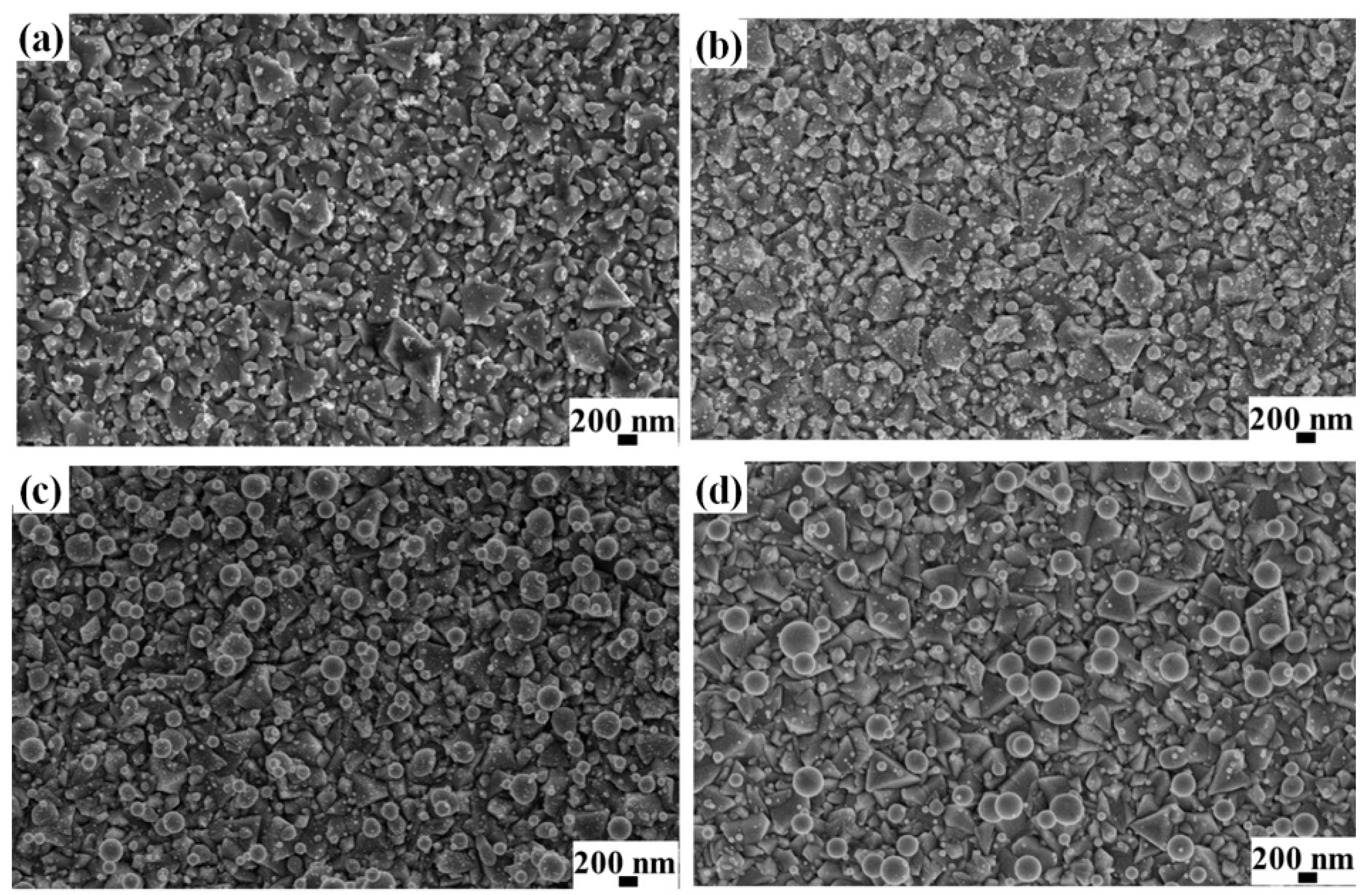
Figure 3.
Representative SEM images of the surface of the as-deposited FTO (substrate A) on which the AuPd film is deposited with increasing the amount of deposited AuPd: (a) 4.3 nm; (b) 7.5 nm; (c) 29.2 nm; and (d) 48.6 nm.
Figure 3.
Representative SEM images of the surface of the as-deposited FTO (substrate A) on which the AuPd film is deposited with increasing the amount of deposited AuPd: (a) 4.3 nm; (b) 7.5 nm; (c) 29.2 nm; and (d) 48.6 nm.

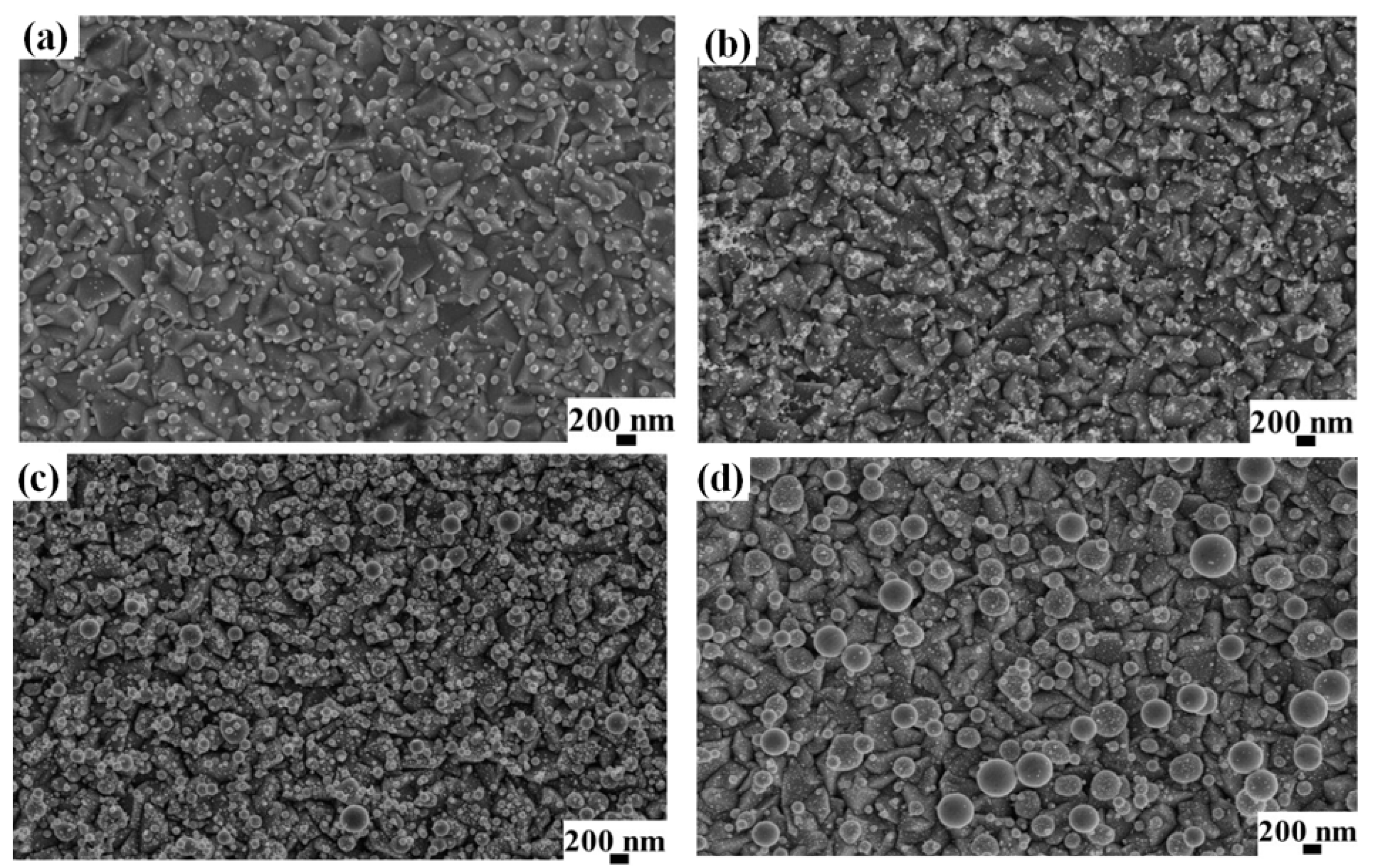
Figure 4.
Representative SEM images of the surface of the textured FTO (substrate B) on which the AuPd film is deposited with increasing the amount of deposited AuPd: (a) 4.3 nm; (b) 7.5 nm; (c) 29.2 nm; and (d) 48.6 nm.
Figure 4.
Representative SEM images of the surface of the textured FTO (substrate B) on which the AuPd film is deposited with increasing the amount of deposited AuPd: (a) 4.3 nm; (b) 7.5 nm; (c) 29.2 nm; and (d) 48.6 nm.

Figure 5.
(a) Optical photo reporting an example of the laser spot as obtained by irradiating the 29.2 nm-thick AuPd film deposited on the textured FTO (substrate B). As pictured in (b), roughly three anular regions can be identified close to the center of the spot and corresponding to an increase of the laser fluence from region 1 to region 3, whereas the maximum laser fluence of 0.5 J/cm2 is obtained in region 3. (c–e) report representative SEM images of the sample surface acquired in region 1 ((c), at a distance >600 µm from the spot center), region 2 ((d), at a distance between 300 and 600 µm from the spot center), and region 3 ((e), at a distance lower than 300 µm from the spot center): this sequence of images clearly shows the dewetting process of the AuPd film.
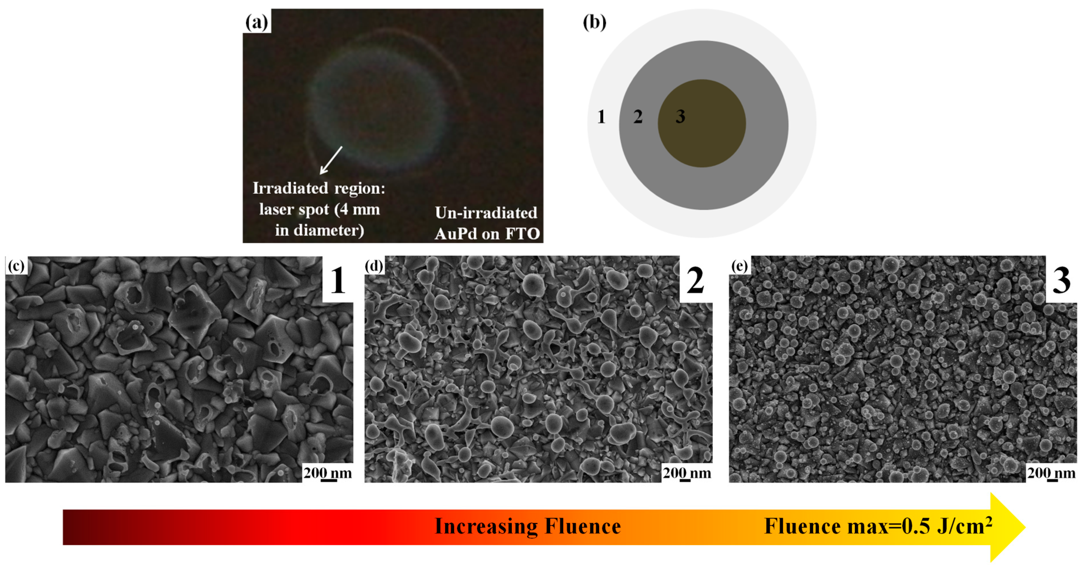
Figure 6.
Enlarged SEM image acquired in on of the spots shown in Figure 5a: the dewetting process is clear by the formation of the spherical nanoparticles from filaments originating from the retreating AuPd film.
Figure 6.
Enlarged SEM image acquired in on of the spots shown in Figure 5a: the dewetting process is clear by the formation of the spherical nanoparticles from filaments originating from the retreating AuPd film.
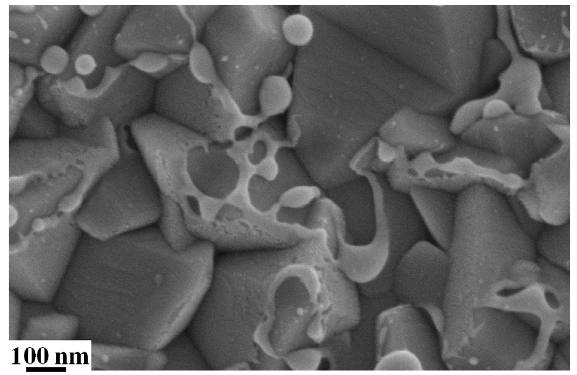
Figure 7.
Representative SEM images, acquired near the laser spot center (i.e., region 3), of the nanoparticles formed by irradiating the AuPd film with thickness 4.3 nm (a), 7.5 nm (b), 29.2 nm (c), and 48.6 nm (d) deposited on the untreated FTO substrate (substrate A).
Figure 7.
Representative SEM images, acquired near the laser spot center (i.e., region 3), of the nanoparticles formed by irradiating the AuPd film with thickness 4.3 nm (a), 7.5 nm (b), 29.2 nm (c), and 48.6 nm (d) deposited on the untreated FTO substrate (substrate A).

Figure 8.
Representative SEM images, acquired near the laser spot center (i.e., region 3), of the nanoparticles formed by irradiating the AuPd film with thickness 4.3 nm (a), 7.5 nm (b), 29.2 nm (c), and 48.6 nm (d) deposited on the textured FTO substrate (substrate B).
Figure 8.
Representative SEM images, acquired near the laser spot center (i.e., region 3), of the nanoparticles formed by irradiating the AuPd film with thickness 4.3 nm (a), 7.5 nm (b), 29.2 nm (c), and 48.6 nm (d) deposited on the textured FTO substrate (substrate B).

Figure 9.
Enlarged SEM images, acquired near the laser spot center (i.e., region 3), of the nanoparticles formed by irradiating the AuPd film with thickness 9.8 nm (a,d), 19.8 nm (b,e), and 48.6 nm (c,f) deposited on the untreated FTO (a–c) and on the textured FTO (d–f).
Figure 9.
Enlarged SEM images, acquired near the laser spot center (i.e., region 3), of the nanoparticles formed by irradiating the AuPd film with thickness 9.8 nm (a,d), 19.8 nm (b,e), and 48.6 nm (c,f) deposited on the untreated FTO (a–c) and on the textured FTO (d–f).
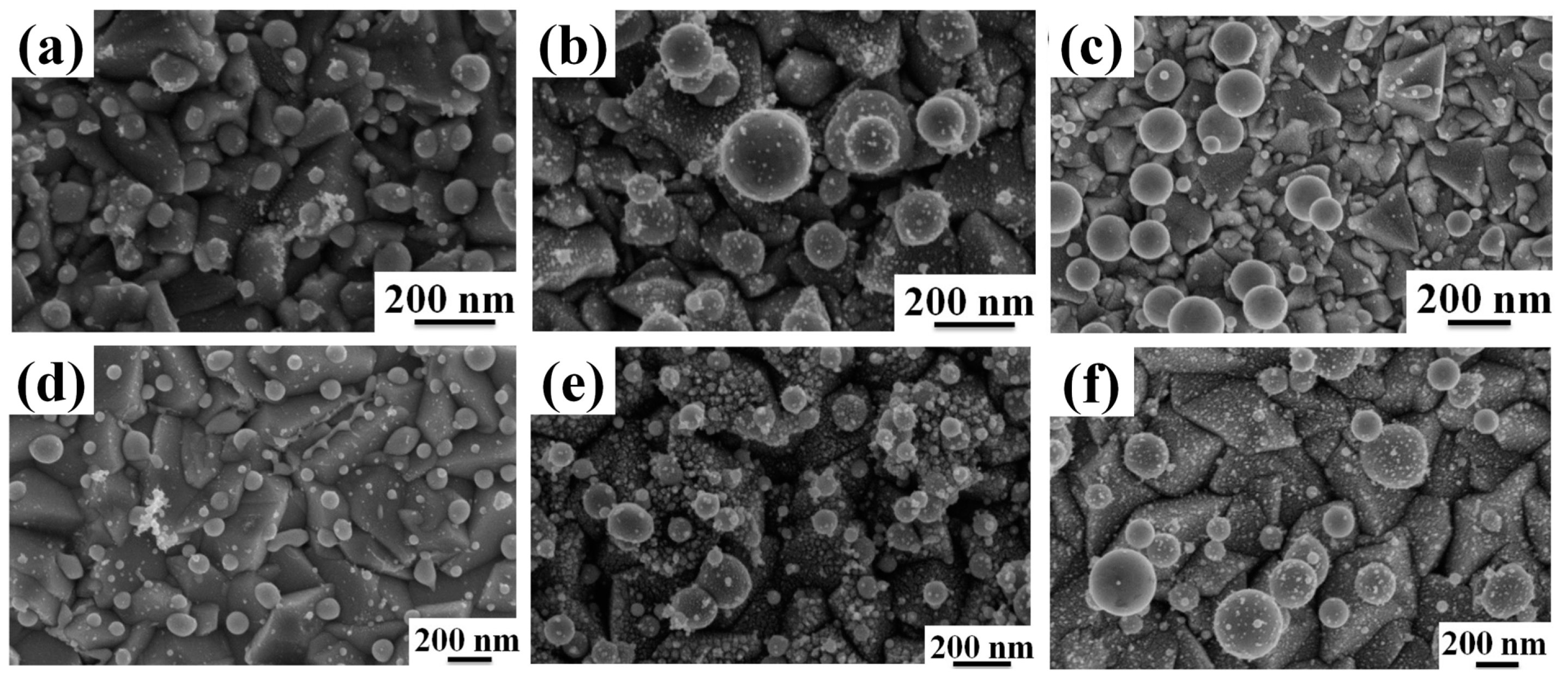
Figure 10.
Log-Log plots of the nanoparticles mean diameter <D> as a function of the starting thickness d of deposited AuPd film on the untreated FTO (substrate A, (a)) and on the textured FTO (substrate B, (b)).
Figure 10.
Log-Log plots of the nanoparticles mean diameter <D> as a function of the starting thickness d of deposited AuPd film on the untreated FTO (substrate A, (a)) and on the textured FTO (substrate B, (b)).

Figure 11.
Log-Log plots of the nanoparticles mean diameter <D> as a function of the starting thickness d of deposited AuPd film on the untreated FTO (substrate A, (a)) and on the textured FTO (substrate B, (b)).
Figure 11.
Log-Log plots of the nanoparticles mean diameter <D> as a function of the starting thickness d of deposited AuPd film on the untreated FTO (substrate A, (a)) and on the textured FTO (substrate B, (b)).
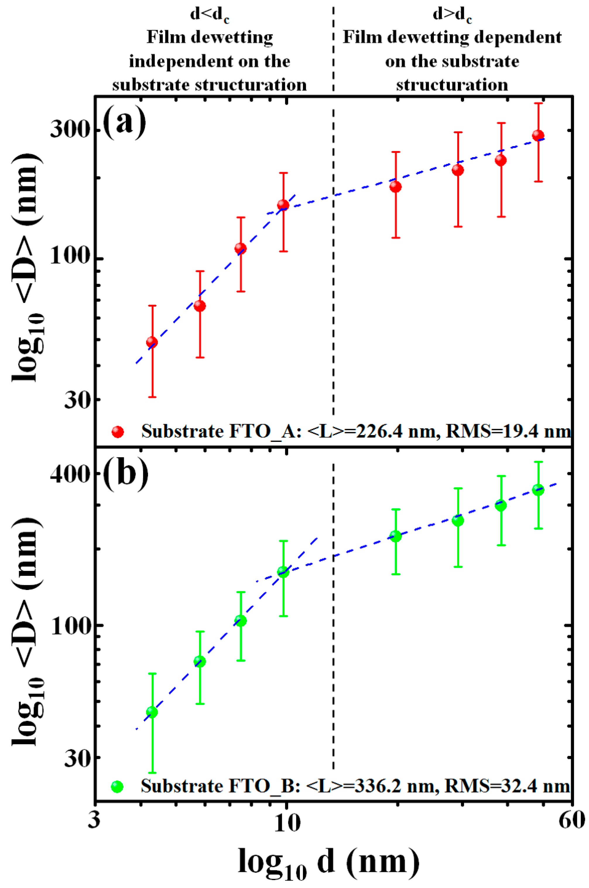
Figure 12.
Pictures of the result of the AuPd dewetting process on the untreated FTO: (a) nanoparticle formation from the dewetting process of the Au film having a thickness d lower than a critical value dc; and (b) nanoparticle formation from the dewetting process of the Au film having a thickness d higher than a critical value dc.
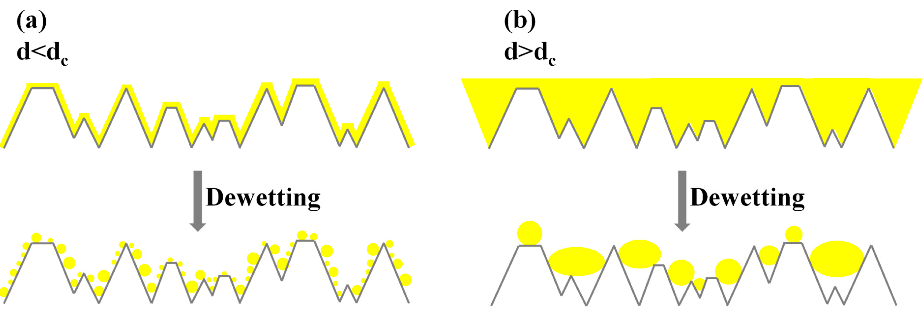
Figure 13.
Pictures of the result of the AuPd dewetting process on the textured FTO: (a) nanoparticle formation from the dewetting process of the Au film having a thickness d lower than a critical value dc; and (b) nanoparticle formation from the dewetting process of the Au film having a thickness d higher than a critical value dc.

Figure 14.
Schematic picture of a conformal film of thickness d deposited on a patterned substrate. The scheme indicates the curvature at the pit edge, RA, and at the inverted apex, RB. The film will evolve to minimize these local curvatures by atomic diffusion from A to B. Reproduced from [48] with permission from the American Institute of Physics.

© 2017 by the author. Licensee MDPI, Basel, Switzerland. This article is an open access article distributed under the terms and conditions of the Creative Commons Attribution (CC BY) license (http://creativecommons.org/licenses/by/4.0/).
Share and Cite
MDPI and ACS Style
Ruffino, F. Experimental Analysis on the Molten-Phase Dewetting Characteristics of AuPd Alloy Films on Topographically-Structured Substrates. Metals 2017, 7, 327. https://doi.org/10.3390/met7090327
AMA Style
Ruffino F. Experimental Analysis on the Molten-Phase Dewetting Characteristics of AuPd Alloy Films on Topographically-Structured Substrates. Metals. 2017; 7(9):327. https://doi.org/10.3390/met7090327
Chicago/Turabian StyleRuffino, Francesco. 2017. "Experimental Analysis on the Molten-Phase Dewetting Characteristics of AuPd Alloy Films on Topographically-Structured Substrates" Metals 7, no. 9: 327. https://doi.org/10.3390/met7090327
Note that from the first issue of 2016, this journal uses article numbers instead of page numbers. See further details here.