Template-Assisted Fabrication of Nanostructured Tin (β-Sn) Arrays for Bulk Microelectronic Packaging Devices


1
Department of Materials Science and Engineering and Department of Energy Systems Research, Ajou University, Suwon 16499, Korea
2
Department of Metallurgical and Materials Engineering, SOE, OP Jindal University, Raigarh 496109, India
3
Department of Mechanical Engineering, Ajou University, Suwon 16499, Korea
*
Author to whom correspondence should be addressed.
Metals 2018, 8(5), 347; https://doi.org/10.3390/met8050347
Submission received: 23 March 2018
/
Revised: 8 May 2018
/
Accepted: 8 May 2018
/
Published: 11 May 2018
(This article belongs to the Special Issue Synthesis and Properties of Bulk Nanostructured Metallic Materials)
Abstract
:In this study, uniform and ordered nanostructured arrays of pure tin (Sn) were produced by the chemical pulse plating method in potentiostatic mode. Bottom metalized anodic aluminium oxide templates were used as the substrates for holding nanostructures during deposition. The plating bath consists of stannous sulfate (SnSO4), sulfuric acid (H2SO4), polyethylene glycol (PEG), and glutaraldehyde as a surfactant. The effect of potentiostatic potential ranging from −0.5 to −3.2 V vs. Ag/AgCl electrode was studied on the growth morphology of nanostructures that were formed. The characterization studies were accomplished by X-ray diffraction (XRD), field emission electron microscopy, and energy dispersive spectroscopy. It was found that several nanostructures were of different shapes and size when the potential was varied. Nanorods were prominent at the deposition potentials of −0.5 and −1.1 V, while a combination of nanostructures (nanorods, nanoplates, and nanoparticles) was predominant at −3.2 V. XRD results show that the nanostructures that were obtained consisted of tetragonal (Sn) structure with a crystallite size of about 20 nm. This process is economically viable and it can be scaled to produce various nanostructures through a careful control of deposition parameters.
1. Introduction
Materials that were prepared on the nanoscale often exhibit many different properties as compared to the same material in their bulk-state. As a result, there has been a tremendous amount of research activities on nanocrystalline materials among engineers and scientists in the past few decades, and the synthesis of bulk nanocrystalline materials is an important topic of recent research on nanocrystalline materials. For example, wire-shaped one-dimensional (1D) nanostructures in microelectronics as chip interconnections as well as fundamental units in functional devices. Especially, the excellent magnetic properties of metallic (Ni-, Fe-, and Co-based) nanostructures have opened new dimensions for next-generation memory devices with a high information storage capacity [1,2,3,4]. The production and the development of metallic or nonmetallic nanostructures are of significant interests due to their advanced application areas, such as microelectronics, optics, sensors, catalysis, fuel cells, solar cells, water purification, thermoelectrics, and bio-implants [5,6,7,8,9,10]. Various nanostructures, 1D or two-dimensional (2D) are synthesized by different routes, such as physical evaporation methods, atomic layer deposition, sonochemical treatment, chemical precipitation methods, polyol methods, ion implantation, and template assisted chemical plating methods [11,12,13,14,15,16,17,18,19,20]. Chemical plating methods where nanostructures are grown in a supporting membrane kind of structure, called templates, are the most popular and simplest methods. The size of the nanowires is generally predetermined by the diameter of the pores inside the templates. In addition, the template-based approach is one of the direct and quick methods to produce nanostructures at the industrial scale [21,22,23]. When compared to chemical methods, physical methods require a great deal of care and handling because they are operated at a fixed temperature and sensitive environment [24,25,26,27]. They are, therefore, not suitable to fill the channels of the templates. In addition, the top-down approach, like physical evaporation or chemical vapor deposition and physical vapor deposition are not desirable to fill up the template pores. This is because of the fact that as soon as the thickness of sputtered atoms rises over the channel openings, most of the pores of the template get blocked. Therefore, a chemical plating method where the nucleation and growth occur from inside the pore walls and bottom is the most suitable for the template based techniques to avoid any kind of pore blockage and high filling efficiency. Among the chemical method, and pulse plating offers many advantages. The pulse plating method is most suitable in view of its various benefits, such as simple and economic procedure as compared to other popular precipitation and sol-gel methods that require processing at high temperatures. The efficiency of plating process can be achieved up to more than 95–99% [12,23]. However, there is a scarcity of literature on Sn nanostructure formation by template-assisted pulse deposition. This may be due to the lack of database and understanding of the various roles of pulse and bath parameters inside the template pores. In addition, high aspect ratio nanostructures can be achieved by changing the template-assisted plating parameters at our will [10,21,22,23,24,25]. Among nanostructures, a more convincing impact of wire-shaped 1D nanosystems is in microelectronics, especially, in chip interconnections and as elemental building blocks in advanced functional devices. Particularly, the remarkable properties of Sn-based nanowires have opened new perspectives to fabricate the next generation of packaging devices [4,5,26,27,28]. For example, the optical transparency of Sn nanowires lies in the range 85–90% and it can be applied as transparent electrodes in electronic devices [28]. Double side tin nanowire arrays have already been tried as advanced thermal interface materials and have possibility for use in future electronic packaging materials [29]. Nanowire-based Sn and Sn-3.5Ag solders have been shown to have better joining characteristics at the nanoscale [30,31]. Therefore, in this work, we have fabricated Sn nanostructures (nanowires, nanorods, nanoplatelets, nanoparticles) in view of their potential applications in recent microelectronic packaging devices. We have used the pulse plating method for nanostructure fabrication using aqueous sulfate bath and an anodic aluminium oxide (AAO) template membrane as cathodic substrate. Further, the effect of varying potential from −0.5 to −3.2 V vs. Ag/AgCl on Sn nanostructure morphology during potentiosatic deposition has been also addressed.
2. Experimental Details
2.1. AAO Template Preparation
Anodic aluminium oxide (AAO) templates (Anodiscs, 60 µm height, Whatmann, Sigma Aldrich, St. Louis, MO, USA) having average pore diameter of 100 nm were used as templates. Prior to deposition, the template was cleaned with distilled water and ethyl alcohol to remove any dirt and grease that is present in the pores, and dried in open air.
2.2. Bath Preparation
The plating bath was prepared for the deposition process by adding the following chemicals procured from Sigma Aldrich (St. Louis, MO, USA) in the composition:
- Stannous Sulfate, SnSO4 (50 g/L, 99.9% pure);
- Sulfuric Acid, H2SO4 (170 g/L, 99.999% pure);
- Polyethylene glycol (PEG), H–(O–CH2–CH2)n–OH, n = 10,000 (g/L, 99.99% pure);
- Glutaraldehyde, OCH(CH2)3CHO (0.025 g/L, 99.99% pure).
The sulfuric acid acts as a supporting electrolyte in the plating bath, while PEG acts as a bath stabilizer. The glutaraldehyde acts as a surfactant additive to provide uniform current distribution and deposition throughout the channels. The surfactant also minimizes the internal stresses in the nanostructures inside the template pores. The bath pH was determined by using a digital pH meter. The bath pH value was around 0.6 ± 0.1 and was operated at room temperature (~26 °C) using an infra-red (IR, ST652, Qingdao Tlead International Co, Ltd., Qingdao, China) thermometer. The plating bath was also kept on stirring at 200 rpm during deposition to have a more uniform distribution of ions in the solution by a SPINOT magnetic stirrer.
2.3. The Plating Cell
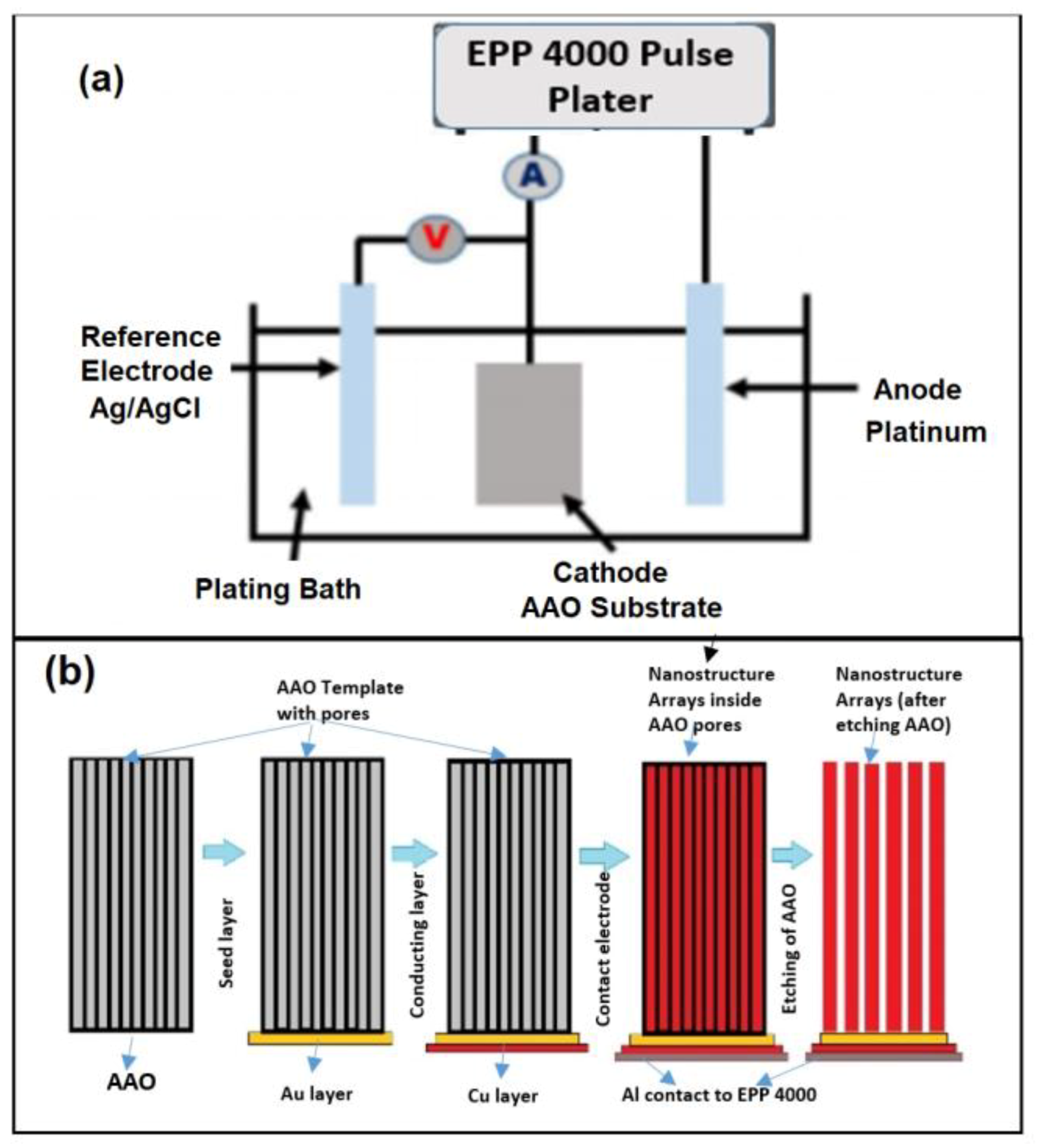
The plating cell was composed three-electrode cell configuration (Figure 1a). AAO template was used as a cathode substrate. Platinum rod was used as a non-consumable anode and an Ag/AgCl that was stabilized with 1 M KCl was used as a standard reference electrode in the plating cell. AAO template was metallized with a thin Au seed layer (150 nm) followed by a Cu layer (500 nm) by a magnetron sputtering inside the channels of the template on one side, as shown in Figure 1b.
The electrode contacts were made by using an Al foil (10 mm) and a conducting silver paste through the template Cu layer. A small area of the Al foil (20 mm × 20 mm) was exposed to the bath solution to complete the circuit among the three-electrode cell.
2.4. The Pulse Plating Experiment
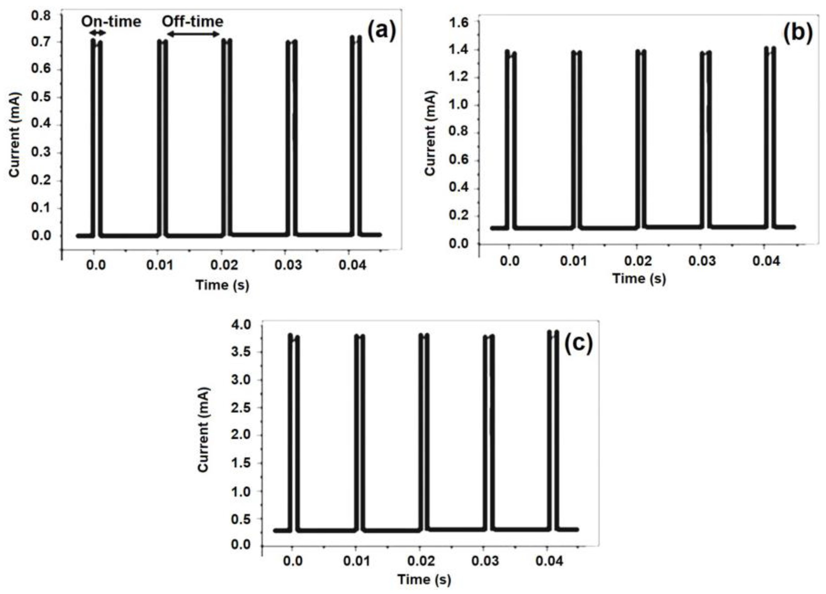
Pulse plating experiment was carried out using the plating bath and immersing the electrodes in it. The electric potential was supplied through Pulse Plater (EPP-4000, Biologic Science Instruments, Seyssinet-Pariset, France). The deposition was carried out under varying potential from −0.5 to −3.2 V vs. Ag/AgCl electrode for a duration of 3 h. Typical current profiles at various potentiostatic potentials are shown in Figure 2, and the corresponding electrical parameters are presented in Table 1. The non-vanishing current at 0 V is due to the side reactions, like hydrogen evolution and/or dissolution of the nanostructures, the current may not reach exactly zero during the off-cycle.
2.5. Recovery of Nanostructures
The AAO template was taken out of the plating bath and was rinsed with distilled water and alcohol and dried. After that, the AAO template was immediately immersed into a 6 M hot solution of KOH for a few minutes. In due course of time, the AAO template was preferentially etched and dissolved out, leaving behind the free-standing array of nanostructures.
3. Microstructural Characterization
3.1. Phase Analysis
The phase analysis of nanostructure arrays was done by X-ray diffraction (XRD) instrument (D2 Phaser Benchtop XRD System, Bruker AXS GmbH, Karlsruhe, Germany) with Co-target operating at 40 kV and 40 mA current. The various peaks obtained in the XRD spectrum were identified by comparison of the peaks with the International Center for Diffraction Data (ICDD) database using TOPAS software module (Version 6, Bruker-AXS, Karlsruhe, Germany) under Pseudo-Voigt profile fitting.
3.2. Nanostructure Morphology
The structure and evolution of Sn nanostructures inside the AAO template were examined using field emission scanning electron microscope (FESEM) (Hitachi 4800, Tokyo, Japan). The compositional analysis was accomplished by using energy dispersive X-ray spectrometer (EDS) that was attached to the FESEM instrument, which was used to identify the elemental compositions that were present in the sample.
4. Results and Discussion
4.1. Phase Evolution
The various phases that are present in the Sn nanostructure arrays after the deposition was analyzed from the XRD spectrum, as shown in Figure 3. The intense peak was noticed at 37.4°, which matches with the (200) plane of the β-Sn lattice. There is another peak at 65.2°, which corresponds to the (301) β-Sn plane. No other peaks of any impurity elements were found in the XRD spectrum, further indicating no contamination from either contact electrodes (Cu, Au, or Al) of the AAO templates.
4.2. Compositional Analysis
The elemental composition of the nanostructures was estimated by the EDS analysis, as shown in Figure 4.
The EDS analysis shows that un-etched sample contains O, Al, and Sn in the spectrum. Al and O are coming from the adhering AAO template while Sn is from the nanostructures inside and on the walls of the AAO (Figure 3a,c,d). The presence of Au is also noticed, which may be from the metalized layer at the bottom that is used as a seed layer. After etching of the AAO template in KOH, there was no trace of elements from metallization layer Cu or Al (Figure 3b,e). This confirms the purity of the obtained free-standing nanostructures by template deposition.
4.3. Morphology of Nanostructures
We divided the range of potential investigated into three categories: (−0.5, −1.1, and −3.2 V), and observed the change in the shape and size of the nanostructures formed. Figure 5 shows the SEM image of the surface morphology of Sn nanostructures that were formed at different potentiostatic potentials. Various types of nanostructures of different shapes and sizes were formed, as shown.
4.3.1. Formation of Short Nanorods (−0.5 V)
Following SEM images show the type and morphology of the Sn nanostructures that were plated at very low potential −0.5 V (Figure 5). The bright nanostructures are visible inside the template pores (Figure 5a–d).
Most of the pores were not filled completely and uneven filing was noticed (Figure 5a). Some of the template pores were half filled and random filling was observed. It can be easily correlated to the very small amount of potential that was fed to the template channels, causing a weaker deposition rate. As a consequence, poor filling of the pores and non-uniform nanorods were produced into the pores. The network of short and fine nanorods was obtained, being aligned along the large axis (Figure 5b). After etching, most of the template material was dissolved, leaving behind few standing nanorods, as shown in (Figure 5c,d). The average diameter of these rod-shaped nanostructures lie within 140–160 nm and the length is rather short in the range of 1–2 µm. This may be due to the poor deposition at this condition rate, as most of the pores are not utilized [21,22,23,24].
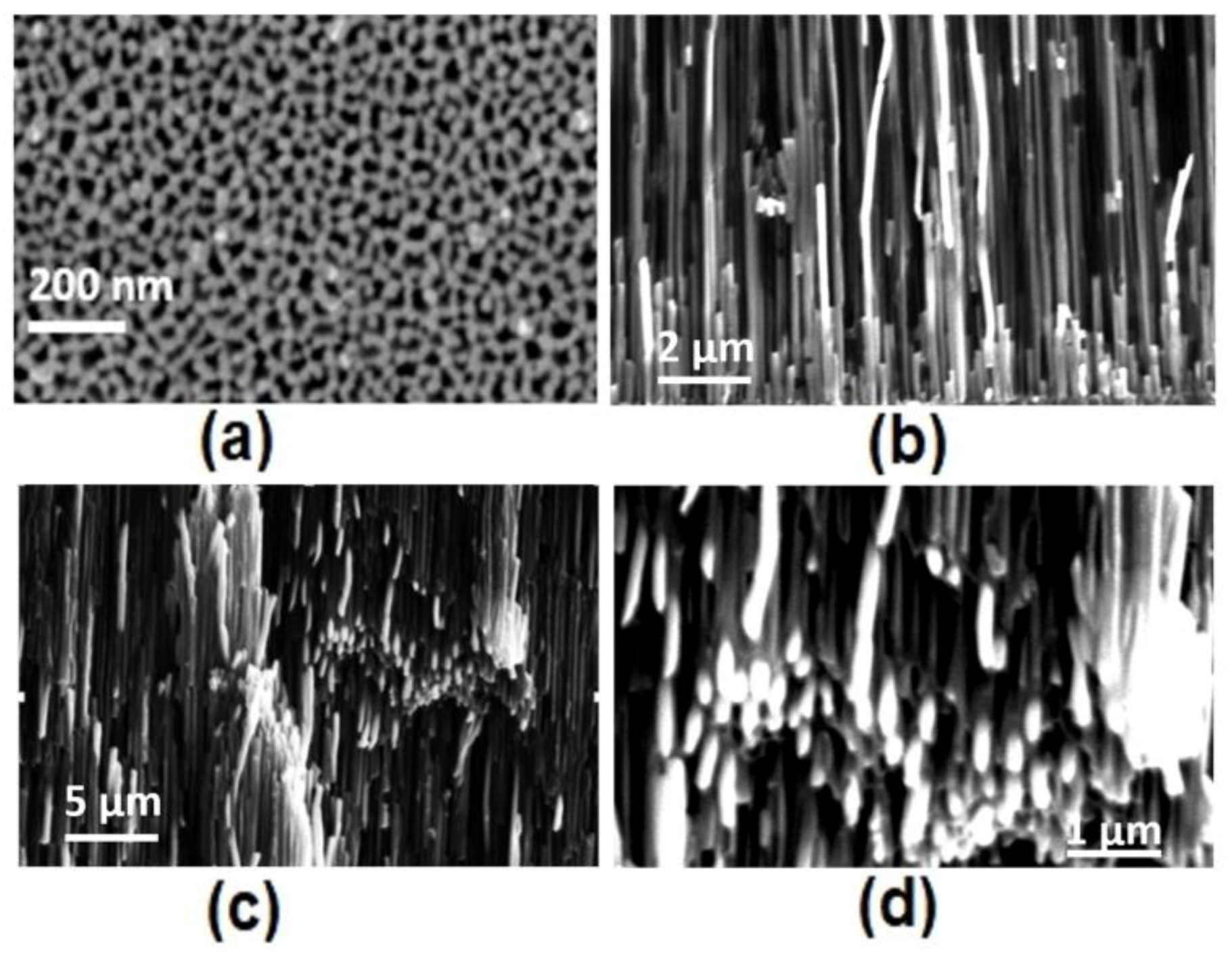
4.3.2. Formation of Large Nanorods/Nanowires (−1.1 V)
The formation of thicker and larger nanorods was noticed when the potential was −1.1 V. Figure 6 shows the well-defined nanorods, which are fully occupied within template pores (Figure 6a,b). A top view of the templates shows the maximum filling of the pores, the white region represents the filled up pores and black spots show the empty pores (Figure 6a). The diameter and length of the nanorods lie in the range of 200 nm and 4–7 µm (Figure 6b–d). The pores are densely filled in most of the cases. The mean diameters of nanorods are larger than the pore diameters of the AAO. This may be due to the fact that these AAO membranes can be slightly dissolved in highly acidic or basic medium solutions [32,33]. Most of the plating baths are highly acidic or basic; the walls of the AAO can be slightly dissolved at higher potentials that are used by electroplating baths.
In addition, the population density of nanostructures also rises with an increase of potential from −0.5 to −1.1 V. The full-fledged nanorods obtained in this potential region are due to the fact that the deposition thickness is enhanced at higher potentials [21]. The nucleation density and the growth rate of nanorods are in proper balance.
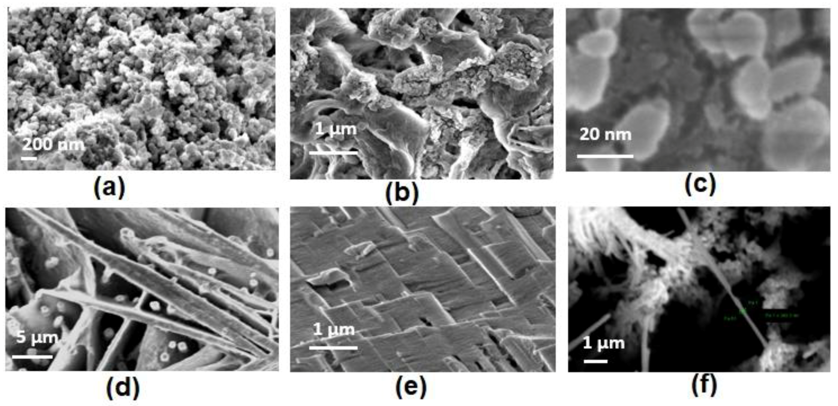
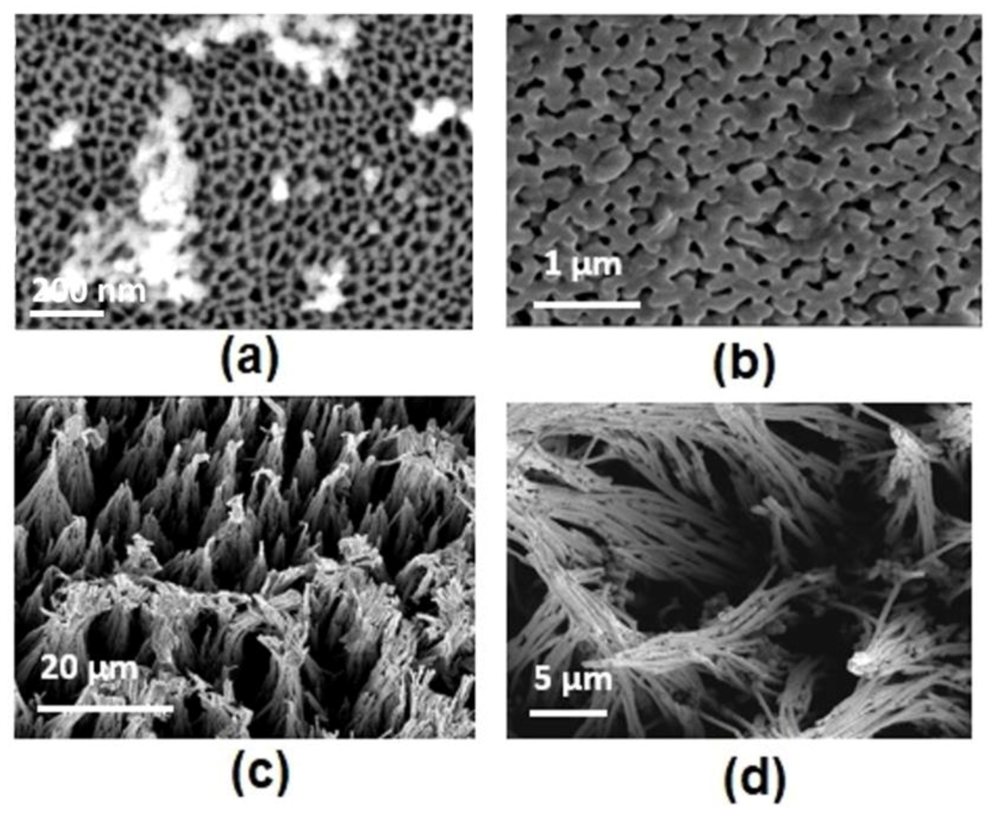
4.3.3. Formation of Nano-Rods, Nanoparticles, and Nanoplates (−3.2 V)
In this case, the deposition potential was further extended to −3.2 V and the morphology was observed, as shown in Figure 7. It can be noticed that a network of various types of nanostructures was formed, being oriented in different directions. We can see nanoparticles, nanoplates, and nanorods (Figure 7a–f) in this case. This can be explained in view of the fact that, an increase in potential to a sufficiently high value, the cathodic polarization increases due to a greater electron movement and reduction in the vicinity of the cathodic layer. A localized deposition triggers the formation of dendrite structures, which may result in fine nanoparticles and nanoplates. The size of the nanoparticles lays around 20–30 nm. The nanorods are 1 μm long and 20 nm wide. At this stage, the electron transfer rate is severe and random, causing a loss of orientation and shape. The nucleation rate rises quickly as compared to growth rate, and multiple nanostructures are noticed.
It can also be noted that the template pores are of fixed dimension and are rigid. Theoretically, the deposition parameters should not affect the size and shape of nanostructures inside the template. The nanostructures are supposed to be confined to the wall surface of the template pores. According to Asli et al. when the pore diameter is below a critical size, layer by layer growth of nanorods occurs, regardless of current density due to a smaller surface area at pore bottom as compared to pore wall [34,35]. Shin et al. commented that, under diffusion limited conditions, the growth of nanowires is independent of system parameters. As the nanowires length increases, the metal ions diffusion into the template pores rises, which make the unstable growth front causing over-deposit and blockage of pores [36,37,38]. Thierry et al. have described that unstable growth of these nanostructures occurs on account of the “tip effect”. The “tip effect” at a higher deposition potential leads to a very high current flow at the tip of the Sn nuclei, which promotes the rapid growth of nanostructures [19].
It is to be noted that, though the deposition takes place inside the pores of AAO template, yet the evolution of hydrogen gas is not prevented in chemical baths during plating. At such higher potential, the inherent hydrogen gas screens the AAO template pores, and hence a number of nanostructures are generated. Top view of the AAO template is shown in Figure 7a, which shows that a maximum amount of pores are filled and the top surface is coated with a Sn layer at higher deposition potential. This is related to the high rates of deposition as well as hydrogen evolution combined to produce the tip effect, and hence multiple nanostructures are formed [19,20,21,36,37,38].
5. Conclusions
There are various conclusions drawn from this study as summarized below:
- 1D Sn nanostructures arrays were produced successfully via the template assisted plating approach from aqueous sulfate bath.
- It was found that the nanostructure shape, size, and morphology were severely affected in response to various deposition potential.
- Low deposition potential of −0.5 V causes formation of very short nanowires (1–2 µm, dia 140–160 nm) and incomplete filling of the AAO template pores is found.
- At a medium deposition potential, −1.1 V, the growth rate of nanostructures was further increased to (4–7 µm length, dia 200 nm). Most of the template pores were filled completely
- As the deposition potential was raised to a sufficiently high value, −3.2 V, multiple nanostructures were formed. The nanoparticles were formed due to the dendritic deposition of Sn inside the AAO template pores (20 nm).
- The multiple nanostructures (nanoplates, nanorods, and nanoparticles) were formed on account of the tip effect of Sn nuclei inside the AAO template. It can be suggested that an optimum deposition potential is needed to exploit the use of each kind of nanostructure and can be potentially controlled for mass production.
Author Contributions
A.S. and B.A. formulated the idea and wrote the manuscript. A.S. performed materials synthesis. A.K.S. and Y.J. performed characterizations. All authors participated in discussion and review of manuscript.
Funding
This research was funded by Basic Science Research Program through the National Research Foundation of Korea (NRF) funded by the Ministry of Science and ICT (NRF-2015R1A2A2A01002387). This research was also supported by the Ajou University research fund.
Acknowledgments
This research was supported by Basic Science Research Program through the National Research Foundation of Korea (NRF) funded by the Ministry of Science and ICT (NRF-2015R1A2A2A01002387). This research was also supported by the Ajou University research fund.
Conflicts of Interest
The authors declare no conflict of interest.
References
- Hernandez-Velez, M. Nanowires and 1D arrays fabrication: An overview. Thin Solid Films 2006, 495, 51–63. [Google Scholar] [CrossRef]
- Vazquez, M.; Pirota, K.; Hernandez-Velez, M.; Prida, V.M.; Navas, D.; Sanz, R.; Batallan, F.; Velazquez, J. Magnetic properties of densely packed arrays of Ni nanowires as a function of their diameter and lattice parameter. J. Appl. Phys. 2004, 95, 6642–6644. [Google Scholar] [CrossRef] [Green Version]
- Djenizian, T.; Hanzu, I.; Eyraud, M.; Santinacci, L. Electrochemical fabrication of tin nanowires: A short review. C. R. Chim. 2008, 11, 995–1003. [Google Scholar] [CrossRef]
- Pang, S.K.; Yung, K.C. A green approach to synthesis of nanoparticles of Sn-3.0Ag-0.5Cu lead-free solder alloy. Mater. Trans. 2012, 53, 1770–1774. [Google Scholar] [CrossRef]
- McAlpine, M.C.; Friedman, R.S.; Jin, S.; Lin, K.H.; Wang, W.U.; Lieber, C.M. High-Performance Nanowire Electronics and Photonics on Glass and Plastic Substrates. Nano Lett. 2003, 3, 1531–1535. [Google Scholar] [CrossRef]
- Bouzigues, C.; Gacoin, T.; Alexandrou, A. Biological applications of rare-earth based nanoparticles. ACS Nano 2011, 5, 8488–8505. [Google Scholar] [CrossRef] [PubMed]
- Sharma, B.; Sharma, A.; Kim, J. Reclamation of diesel oil from sea water using magnetic Au/Fe2O3 nanocomposites prepared by chemical precipitation. Mater. Res. Express 2018, 5, 015047. [Google Scholar] [CrossRef]
- Chena, Z.G.; Hana, G.; Yanga, L.; Chenga, L.; Zoua, J. Nanostructured thermoelectric materials: Current research and future challenge. Prog. Nat. Sci. Mater. Int. 2012, 22, 535–549. [Google Scholar] [CrossRef]
- Aghiu, M.A.; Gorea, M.; Kristaly, F.; Tomoaia-Cotisel, M. A new method for synthesis of forsterite nanomaterials for bioimplants. Ceram. Silik. 2014, 58, 303–307. [Google Scholar]
- Sharma, B.; Sharma, A.; Kim, J.S. Recent Advances on H 2 Sensor Technologies Based on MOX and FET Devices: A Review. Sens. Actuators B Chem. 2018, 262, 758–770. [Google Scholar] [CrossRef]
- Nguyen, V.H. Nanomaterials: A guide to fabrication and applications. Adv. Nat. Sci Nanosci. Nanotechnol. 2017, 8, 020401. [Google Scholar]
- Schlesinger, M.; Paunovic, M. Modern Electroplating, 5th ed.; John Wiley and Sons, Inc.: Hoboken, NJ, USA, 2010. [Google Scholar]
- Sharma, A.; Cheon, C.S.; Jung, J.P. Recent progress in electroless plating of copper. J. Microelectron. Packag. Soc. 2016, 23, 1–6. [Google Scholar] [CrossRef]
- Li, R.; Sun, X.; Zhou, X.; Cai, M.; Sun, X. Aligned Heterostructures of Single-Crystalline Tin Nanowires Encapsulated in Amorphous Carbon Nanotubes. J. Phys. Chem. C 2007, 111, 9130–9135. [Google Scholar] [CrossRef]
- Zhou, Q.; Liu, X.; Zhao, Y.; Jia, N.; Liu, L.; Yan, M.; Jiang, Z. Single crystal tin nano-rod arrays electrodeposited by a soft template. Chem. Commun. 2005, 4941–4942. [Google Scholar] [CrossRef] [PubMed]
- Qui, L.; Vilas, G.P.; Jose, C.M.; Aharon, G. Synthesis of tin nanorods via a sonochemical method combined with a polyol process. Ultrason. Sonochem. 2005, 12, 243–247. [Google Scholar]
- Johansson, A. Template-Based Fabrication of Nanostructured Materials. Ph.D. Thesis, Upssala University, Upssala, Sweden, 2006. [Google Scholar]
- Sharma, A.; Jang, Y.J.; Jung, J.P. Effect of KOH to Na2SiO3 ratio on microstructure and hardness of plasma electrolytic oxidation coatings on AA 6061 alloy. J. Mater. Eng. Perform. 2017, 26, 5032–5042. [Google Scholar] [CrossRef]
- Thierry, D.; Ilie, H.; Yesudas, D.P.; Florence, V.; Philippe, K. Electrochemical fabrication of Sn nanowires on titania nanotube guide layers. Nanotechnology 2008, 19, 205601. [Google Scholar]
- Lin, J.Y.; Yu, L.H.; Huang, J.J.; Wu, J.R. Effect of silver nitrate concentration of silver nanowires synthesized using a polyol method and their application as transparent conductive films. Thin Solid Films 2015, 584, 243–247. [Google Scholar] [CrossRef]
- Sharma, A.; Bhattacharya, S.; Das, S.; Das, K. A study on the effect of pulse electrodeposition parameters on the morphology of pure tin coatings. Metall. Mater. Trans. A 2014, 45, 4610–4622. [Google Scholar] [CrossRef]
- Rashidi, A.M.; Amadeh, A. The effect of current density on the grain size of electrodeposited nanocrystalline nickel coatings. Surf. Coat. Technol. 2008, 202, 3772–3776. [Google Scholar] [CrossRef]
- Schlesinger, M.; Paunovic, M. Fundamental of Electrochemical Deposition, 2nd ed.; John Wiley & Sons, Inc.: Hoboken, NJ, USA, 2006. [Google Scholar]
- Zhang, H.; Jiang, F.; Zhou, R.; Du, Y.; Yang, P.; Wang, C.; Xu, J. Effect of deposition potential on the structure and electrocatalytic behavior of Pt micro/nanoparticles. Int. J. Hydrogen Energy 2011, 36, 15052–15059. [Google Scholar] [CrossRef]
- Schmitz, E.P.S.; Quinaia, S.P.; Garcia, J.R.; de Andrade, C.K.; Lopes, M.C. Influence of commercial organic additives on the nickel electroplating. Int. J. Electrochem. Sci. 2016, 11, 983–997. [Google Scholar]
- Shin, H.S.; Song, J.Y.; Yu, J. Lattice Deformation of Sn Nanowires for the Application to Nano-Interconnection Technology. In Proceedings of the 60th International Conference on ‘IEEE Electronic Components and Technology’, Las Vegas, NV, USA, 1–4 June 2010; pp. 1861–1865. [Google Scholar]
- Cui, Q.; Rajathurai, K.; Jia, W.; Li, X.; Gao, F.; Lei, Y.; Gu, Z. Synthesis of Single Crystalline Tin Nanorods and Their Application as Nanosoldering Materials. J. Phys. Chem. C 2010, 114, 21938–21942. [Google Scholar] [CrossRef]
- Cai, H.; Wang, W.; Liu, P.; Wang, G.; Liu, A.; He, Z.; Cheng, Z.; Zhang, S.; Xia, M. Enhanced synthesis of Sn nanowires with aid of Se atom via physical vapor transport. J. Cryst. Growth 2015, 420, 42–46. [Google Scholar] [CrossRef]
- Feng, B.; Faruque, F.; Bao, P.; Chien, A.T.; Kumar, S.; Peterson, G.P. Double-sided tin nanowire arrays for advanced thermal interface materials. Appl. Phys. Lett. 2013, 102, 093105. [Google Scholar] [CrossRef]
- Zhang, H.; Zhang, J.; Lan, Q.; Ma, H.; Qu, K.; Inkson, B.J.; Mellors, N.J.; Xue, D.; Peng, Y. Nanoscale characterization of 1D Sn-3.5Ag nanosolders and their application into nanowelding at the nanoscale. Nanotechnology 2014, 25, 425301. [Google Scholar] [CrossRef] [PubMed]
- Li, Q.; Liu, G.; Yang, H.; Wang, W.; Luo, S.; Dai, S.; Qiu, M. Sn nanowires can be used in low temperature soldering. Appl. Phys. Lett. 2016, 108, 193101. [Google Scholar] [CrossRef]
- Tian, Y.T.; Meng, G.W.; Gao, T.; Sun, S.H.; Xie, T.; Peng, X.S.; Ye, C.H.; Zhang, L.D. Alumina nanowire arrays standing on a porous anodic alumina membrane. Nanotechnology 2004, 15, 189–191. [Google Scholar] [CrossRef]
- Xiao, Z.L.; Han, C.Y.; Welp, U.; Wang, H.H.; Kwok, W.K.; Willing, G.A.; Hiller, J.M.; Cook, R.E.; Miller, D.J.; Crabtree, G.W. Fabrication of alumina nanotubes and nanowires by etching porous alumina Membranes. Nano Lett. 2002, 2, 1293–1297. [Google Scholar] [CrossRef]
- Ertan, A.; Tiwari, S.N.; Talu, O. Electrodeposition of Nickel Nanowires and Nanotubes Using Various Templates. J. Exp. Nanosci. 2008, 3, 287–295. [Google Scholar] [CrossRef]
- Shin, S.; Al-Housseiny, T.T.; Kim, B.S.; Cho, H.H.; Stone, H.A. The Race of Nanowires: Morphological Instabilities and a Control Strategy. Nano Lett. 2014, 14, 4395–4399. [Google Scholar] [CrossRef] [PubMed]
- Chandrasekar, M.S.; Pushpavanam, M. Pulse and pulse reverse plating—Conceptual, advantages and applications. Electrochim. Acta 2008, 53, 3313–3322. [Google Scholar] [CrossRef]
- Inguanta, R.; Ferrara, G.; Piazza, S.; Sunseri, C. Nanostructures fabrication by template deposition into anodic alumina membranes. Chem. Eng. Trans. 2009, 17, 957–962. [Google Scholar]
- Shin, S.; Kim, B.S.; Kim, K.M.; Kong, B.H.; Cho, H.K.; Cho, H.H. Tuning the morphology of copper nanowires by controlling the growth processes in electrodeposition. J. Mater. Chem. 2011, 21, 17967–17971. [Google Scholar] [CrossRef]
Figure 1.
(a) Pulse plating experimental set up and (b) schematic illustration for template assisted plating.
Figure 1.
(a) Pulse plating experimental set up and (b) schematic illustration for template assisted plating.

Figure 2.
The current profile used for the various potentiostatic potential (a) −0.5 V; (b) −1.1 V; and (c) −3.2 V.
Figure 2.
The current profile used for the various potentiostatic potential (a) −0.5 V; (b) −1.1 V; and (c) −3.2 V.

Figure 3.
X-ray diffraction (XRD) spectrum of the free-standing Sn nanostructure arrays.

Figure 4.
Energy dispersive X-ray spectrometer (EDS) Spectrum of Sn nanostructures array (a) secondary electron (SE) image of the top view of the template before etching; (b) SE image of the side view of the nanostructure after template etching; (c) EDS spectrum with anodic aluminium oxide (AAO) template with empty pores before etching; (d) EDS spectrum of the AAO template where the pores were filled before etching; (e) EDS spectrum of the nanostructure after template etching.
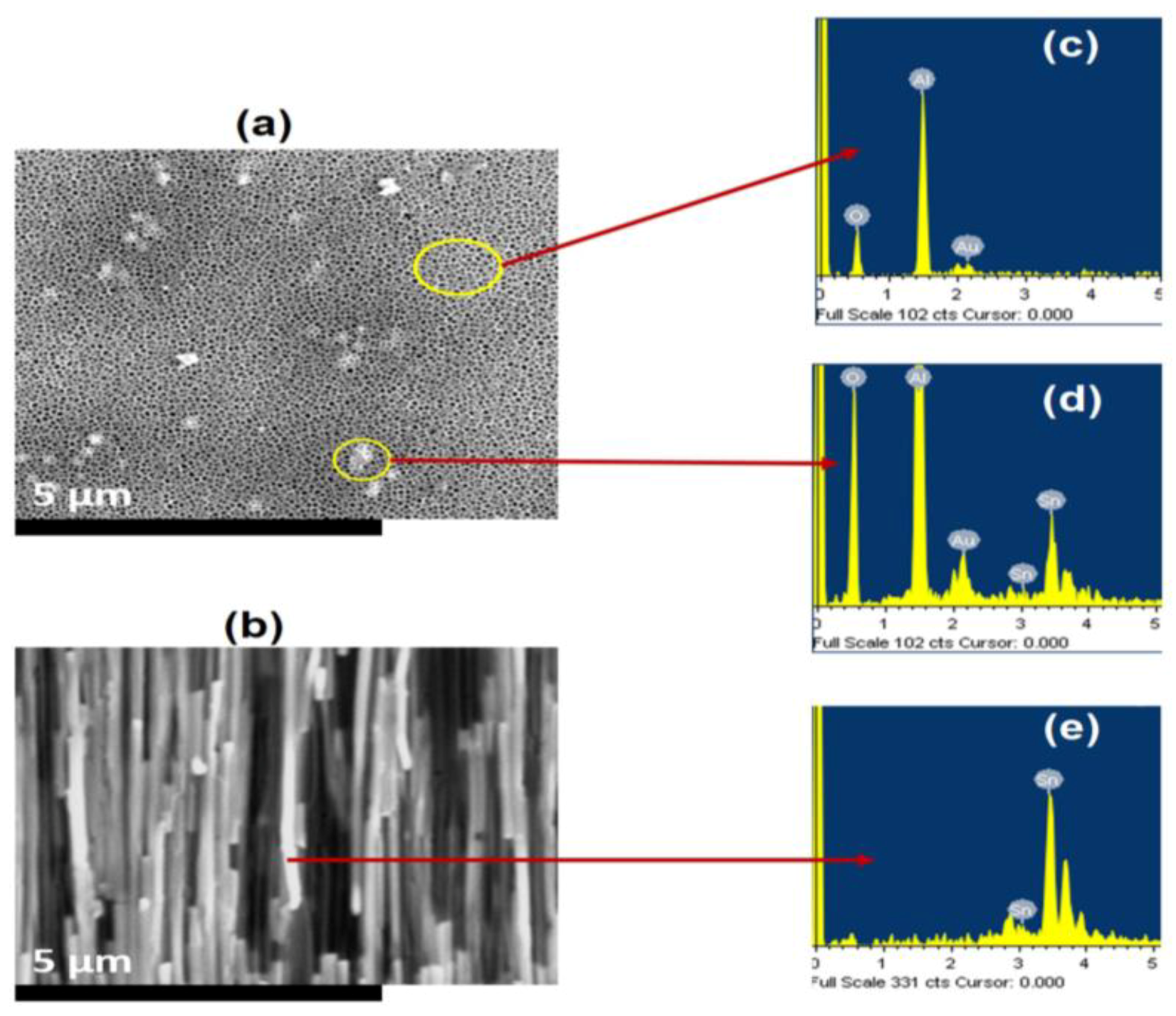
Figure 5.
Field emission scanning electron microscope (FESEM) micrograph of random oriented nanorods at potential of −0.5 V (a) top view of the AAO template; (b) cross section of the AAO template; (c) cross-section of AAO template at another location; and (d) higher resolution image of (c).
Figure 5.
Field emission scanning electron microscope (FESEM) micrograph of random oriented nanorods at potential of −0.5 V (a) top view of the AAO template; (b) cross section of the AAO template; (c) cross-section of AAO template at another location; and (d) higher resolution image of (c).

Figure 6.
FESEM micrograph of highly ordered nanorods at potential of −1.1 V (a) top view of the AAO template; (b) Another top view of un-even deposits of nanostructures; (c) cross-section of the AAO template showing dense array of nanorods; and (d) a higher resolution image of the (c).
Figure 6.
FESEM micrograph of highly ordered nanorods at potential of −1.1 V (a) top view of the AAO template; (b) Another top view of un-even deposits of nanostructures; (c) cross-section of the AAO template showing dense array of nanorods; and (d) a higher resolution image of the (c).

Figure 7.
FESEM micrograph of randomly oriented multiple nanostructures at potential of −3.2 V (a) top view of the AAO template; (b) high resolution of the (a); (c) high resolution image of (b) showing a cluster of nanoparticles; (d) formation of nanoplates and nanoparticles inside the template at few locations, tilted view of (d); (e) a close view of the nanoplates in (d); and (f) formation of random nanorods of uneven thickness.

Table 1.
Experimental conditions and pulse parameters.
| Parameters | Values |
|---|---|
| pH | 0.6 |
| Applied potential | −0.5 V, −1.1 V, −3.2 V |
| Off time potential | 0 |
| On-time, Off-time | 0.001 s, 0.01 s |
| Temperature | 26 °C |
| Duty Cycle | 10% |
| Frequency | 100 Hz |
© 2018 by the authors. Licensee MDPI, Basel, Switzerland. This article is an open access article distributed under the terms and conditions of the Creative Commons Attribution (CC BY) license (http://creativecommons.org/licenses/by/4.0/).
Share and Cite
MDPI and ACS Style
Sharma, A.; Srivastava, A.K.; Jeon, Y.; Ahn, B. Template-Assisted Fabrication of Nanostructured Tin (β-Sn) Arrays for Bulk Microelectronic Packaging Devices. Metals 2018, 8, 347. https://doi.org/10.3390/met8050347
AMA Style
Sharma A, Srivastava AK, Jeon Y, Ahn B. Template-Assisted Fabrication of Nanostructured Tin (β-Sn) Arrays for Bulk Microelectronic Packaging Devices. Metals. 2018; 8(5):347. https://doi.org/10.3390/met8050347
Chicago/Turabian StyleSharma, Ashutosh, Ashok K. Srivastava, Yongho Jeon, and Byungmin Ahn. 2018. "Template-Assisted Fabrication of Nanostructured Tin (β-Sn) Arrays for Bulk Microelectronic Packaging Devices" Metals 8, no. 5: 347. https://doi.org/10.3390/met8050347
Note that from the first issue of 2016, this journal uses article numbers instead of page numbers. See further details here.