1. Introduction
As the microwave (MW) spectrum becomes more and more crowded, which is synonymous with an increasing electromagnetic (EM) compatibility problem [
1], one needs new functional materials for EM coatings, shields and filters, working in specific frequency bands. Such materials should combine high electrical conductivity with good electromagnetic interference (EMI) shielding efficiency (SE), the reciprocal of the transmittance. Small sheet resistance, high optical and IR transparency, ultra-small thickness and ultra-light weight make graphene [
2] an excellent candidate for designing such poly-functional materials for EM applications.
Microwave probing has revealed that even a single graphene monolayer is capable of providing almost 20% of EM attenuation [
3]. However, since deposition of graphene on dielectric surfaces of arbitrary shape is still a difficult task, attention of scientists and engineers is currently focused on composite materials filled with graphene nanoplatelets, nanoribbons and flakes that also demonstrate remarkable mechanical, thermal and electromagnetic properties (see [
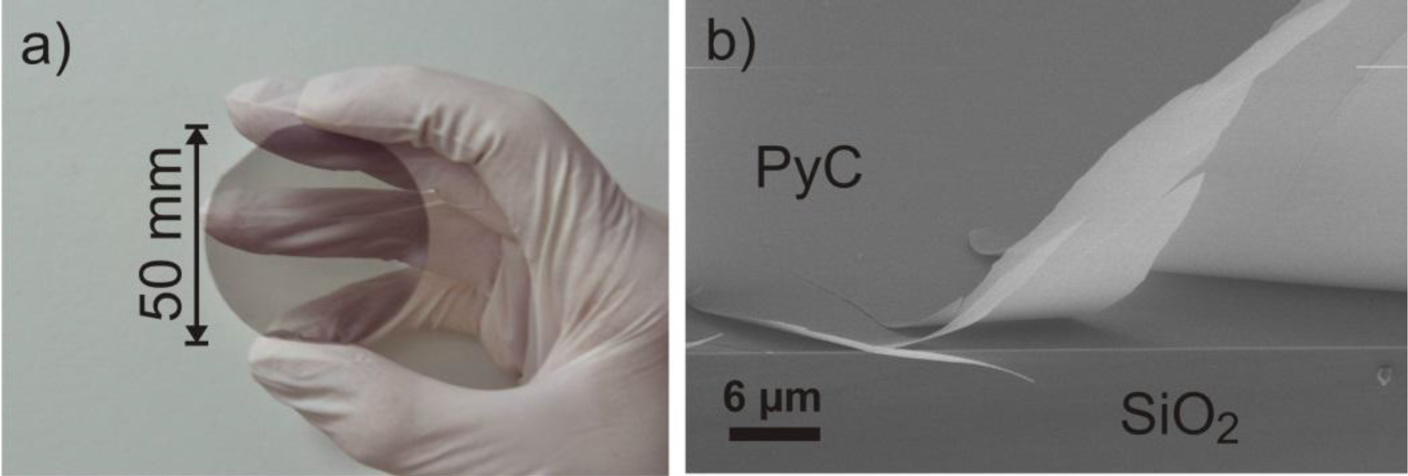
4] and references therein). We have recently suggested an interesting alternative to graphene-based materials by demonstrating that 25 nm thick pyrolytic carbon (PyC) film, which is morphologically close to the nanographite, being many thousands times thinner than skin depth can attenuate a significant part of incident microwave radiation [
5]. In contrast to graphene, PyC films can be easily synthesized not only on metal, but also on dielectric substrate [
6] of arbitrary shape which makes it very attractive from the technological point of view. Moreover, being 5–100 times thicker than graphene monolayers, PyC film are much more robust than atom layer thick graphene,
i.e., it is hardly influenced by mechanical tension, acoustic waves or an external electric field. The EM response of PyC films can be easily described and characterized in the framework of the conventional techniques allowing quantitative description of their properties. It is also worth noting that coating of a substrate with PyC film is much cheaper than with graphene,
i.e., PyC films are also commercially attractive for a wide range of applications.
The frequency dependence of transmittance/reflectance in K
a-band, 26–37 GHz, for 25 nm thick PyC film was measured in [
5]. An experiment demonstrated surprisingly high absorbance (~30%) despite the small sample thickness, which was many thousands times less than the skin depth in metals. The experimental and theoretical description of transmittance/reflectance of PyC films of different thicknesses at the frequency of 30 GHz has been reported recently in our paper [
7]. In the current paper, we concentrate on the frequency dependence of absorption, transmission and reflection of PyC films in the K
a-band (26–37 GHz). In particular, we address two important points for practical application: (i) dependence of the absorbance/reflectance of PyC film deposited on quartz substrate on the irradiation effect from the PyC or substrate side; and (ii) frequency dependence of the EM properties of binary PyC-quartz structures in the K
a-band.
3. Theory
The longitudinal component of magnetic field associated with a TE waveguide mode is described by the following equation:
where + and − correspond to the waves propagating along waveguide axis
z in positive and negative directions, respectively, subscript
i = 0, 1, 2, 3 labels vacuum, substrate, PyC film and vacuum, respectively,
x,
y are cross sectional coordinates of the rectangular waveguide,
kx =
![Applsci 04 00255 i009]()
,
ky =
![Applsci 04 00255 i010]()
, where
a,
b are the lateral waveguide dimensions,
n,
m are integers,
Ki =
![Applsci 04 00255 i011]()
is the longitudinal wavenumber in the
i-th medium,
bi is mode amplitudes in
i-th medium to be found from boundary conditions. In particular, if the waveguide supports TE
1,0 mode,
n = 1,
m = 0 and
Ki =
![Applsci 04 00255 i012]()
.
Let us consider the “quartz + PyC” geometry when the EM wave is incident on the quartz substrate. Boundary conditions in this geometry have the following form [
7]:
Here
l1 and
l2 are the thicknesses of substrate and PyC film, respectively. By solving Equation (2) under assumptions
K2l2 << 1, Im{
ε2} >> 1 and |
K2|
2 >>
K1K0 we arrive at the following equations for the complex transmission (
t =
![Applsci 04 00255 i013]()
) and reflection (
r =
![Applsci 04 00255 i014]()
) coefficients in the “quartz + PyC” geometry:
Where
ϕ =
K1l1 is the phase accrued by the wave after one pass through the substrate,
R0 = |
K1 −
K0|
2 / |
K1 +
K0|
2 and
T0 = 4
K1K0 / |
K1 +
K0|
2 are reflectance and transmittance of the vacuum-substrate interface, respectively, δ =
l2/
lσ where
lσ =
c2(
K0 −
K1)/4πωσ is the characteristic length that describe EM properties of the two-layer structure.
In order to clarify the meaning of
lσ it is instructive to consider the interaction of the EM with a free standing thin conductive film. In such a case the amplitude reflection/transmission coefficients can be obtained from Equation (2) at
K0 =
K1 and
l1 = 0. By substituting
T0 = 1 and
R0 =
ϕ = 0 into Equation (3) we arrive at the following equations for the transmittance and reflectance of the conductive film with thickness
l2:
One can observe from Equation (4) that at
l2 =
lσ absorption losses in the film are maximum and
A = 0.5.
In the “PyC + quartz” geometry, the amplitude transmission coefficient (and, hence, transmittance) is expectedly the same as that in the “quartz + PyC” geometry. However the complex reflection coefficients (and hence reflectance and absorbance) are different in “quartz + PyC” and “PyC + quartz” geometries:
Thus one can conclude that overall shielding efficiency, which is determined by the transmittance, does not depend on which side of the substrate the absorbing coating is deposited. However the reflectance and hence absorbance of such two-layer structure do depend on the geometry chosen.
It also follows from Equation (5) that at a finite substrate thickness, the transmittance and reflectance is affected by the interference of the EM wave in the substrate. In our experimental conditions, we cannot expect strong oscillations in the reflected and transmitted waves because the phase accrued by the wave after one pass through the substrate varies from 0.05π to about 0.1π over the studied spectral range. However the interference effects can strongly influence the amount of the reflected and absorbed EM energy because it is determined by the EM wave amplitude inside the PyC film.
4. Results and Discussion
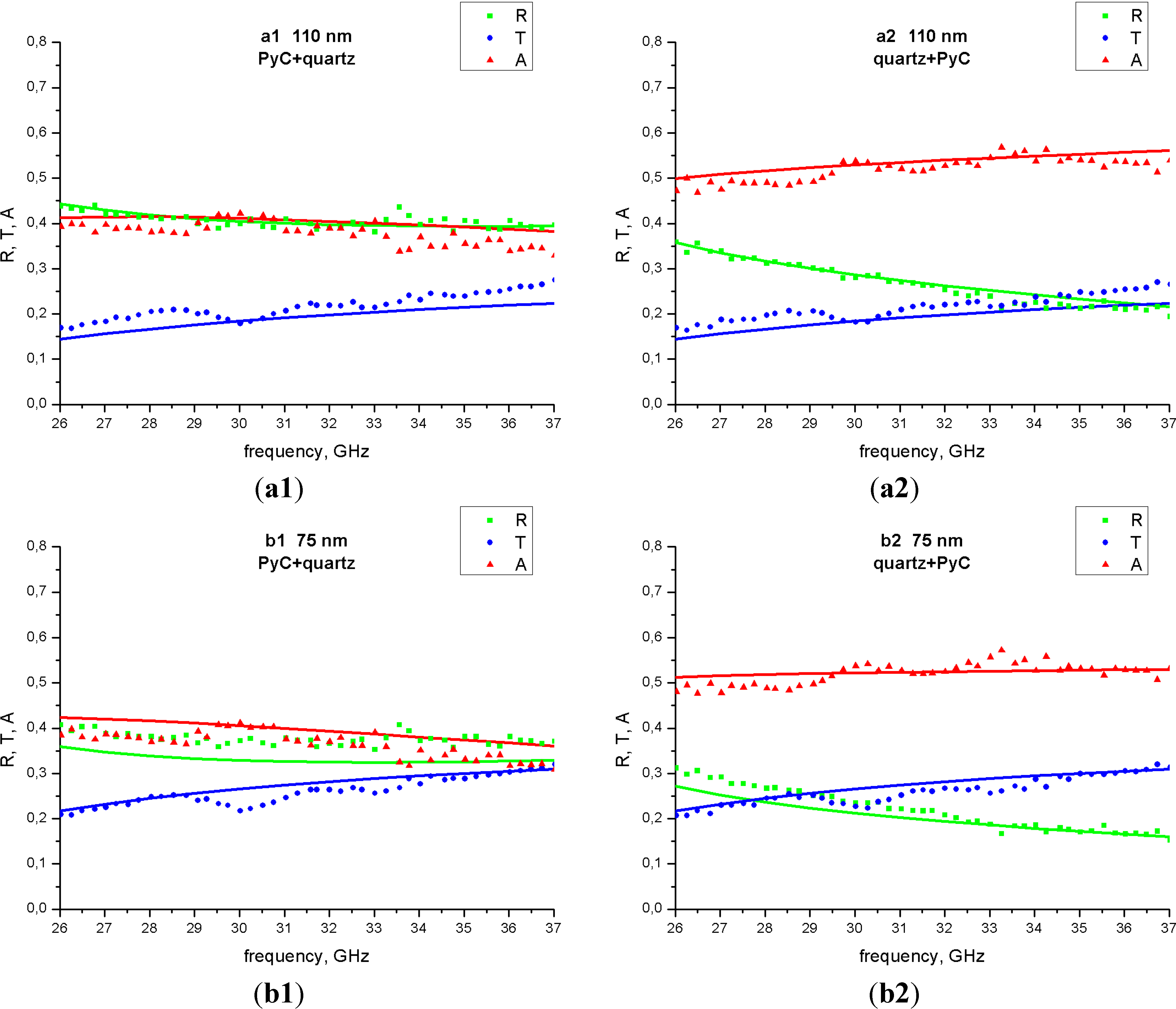
In the numerical calculations the following parameters were used: permittivity of substrate ε1 = 3.5, PyC film conductivity σ = 4.5 × 10¹⁴ s−1 (5.0 × 10⁴ S/m), lateral waveguide dimensions are a = 7.2 mm, b = 3.4 mm.
The measured and calculated reflectance, transmittance and absorbance are presented in
Figure 3 for films being 75 nm and 110 nm thick and in
Table 2 for thinner films (9 nm, 20 nm and 30 nm).
Comparison of experimental data with results of calculations in the frequency range 26–37 GHz shows the metal-like behavior of PyC. One can notice that in the “PyC + quartz” geometry, 110 nm thick PyC film is capable to absorb not more than 40% of incident power, whereas in the “quartz + PyC” geometry, the absorption losses are as high as 50%–55%. Thus the latter geometry can be employed to improve sensitivity of the detectors of MW radiation.
Figure 3.
Calculated (solid lines) and measured (circles, squares and triangles) reflectance, transmittance and absorbance spectra of 110 nm (a1, a2) and 75 nm (b1, b2) thick films in the “PyC + quartz” (a1, b1) and “quartz + PyC” (a2, b2) geometries.
Figure 3.
Calculated (solid lines) and measured (circles, squares and triangles) reflectance, transmittance and absorbance spectra of 110 nm (a1, a2) and 75 nm (b1, b2) thick films in the “PyC + quartz” (a1, b1) and “quartz + PyC” (a2, b2) geometries.
Table 2.
Theoretical (subscript “th”) and experimental (subscript “exp”) transmittance, reflectance and absorbance for thinnest PyC films on SiO2 substrate.
Table 2.
Theoretical (subscript “th”) and experimental (subscript “exp”) transmittance, reflectance and absorbance for thinnest PyC films on SiO2 substrate.
| Frequency, GHz | PyC Thickness, 9 nm |
|---|
| Rexp | Rth | Texp | Tth | Aexp | Ath |
|---|
| 26 | 0.19 | 0.19 | 0.65 | 0.63 | 0.16 | 0.18 |
| 30 | 0.18 | 0.17 | 0.67 | 0.67 | 0.16 | 0.16 |
| 32 | 0.17 | 0.17 | 0.68 | 0.68 | 0.16 | 0.15 |
| 34 | 0.17 | 0.17 | 0.69 | 0.68 | 0.14 | 0.15 |
| 36 | 0.16 | 0.18 | 0.69 | 0.68 | 0.15 | 0.14 |
| Frequency, GHz | PyC Thickness, 20 nm |
| Rexp | Rth | Texp | Tth | Aexp | Ath |
| 26 | 0.18 | 0.17 | 0.49 | 0.51 | 0.33 | 0.32 |
| 30 | 0.15 | 0.15 | 0.51 | 0.56 | 0.34 | 0.29 |
| 32 | 0.14 | 0.15 | 0.54 | 0.57 | 0.32 | 0.28 |
| 34 | 0.13 | 0.15 | 0.57 | 0.58 | 0.29 | 0.28 |
| 36 | 0.13 | 0.15 | 0.57 | 0.58 | 0.31 | 0.27 |
| Frequency, GHz | PyC Thickness, 30 nm |
| Rexp | Rth | Texp | Tth | Aexp | Ath |
| 26 | 0.20 | 0.17 | 0.40 | 0.43 | 0.40 | 0.40 |
| 30 | 0.16 | 0.14 | 0.41 | 0.48 | 0.43 | 0.38 |
| 32 | 0.14 | 0.14 | 0.45 | 0.49 | 0.41 | 0.37 |
| 34 | 0.13 | 0.14 | 0.48 | 0.50 | 0.39 | 0.36 |
| 36 | 0.13 | 0.14 | 0.50 | 0.51 | 0.38 | 0.35 |
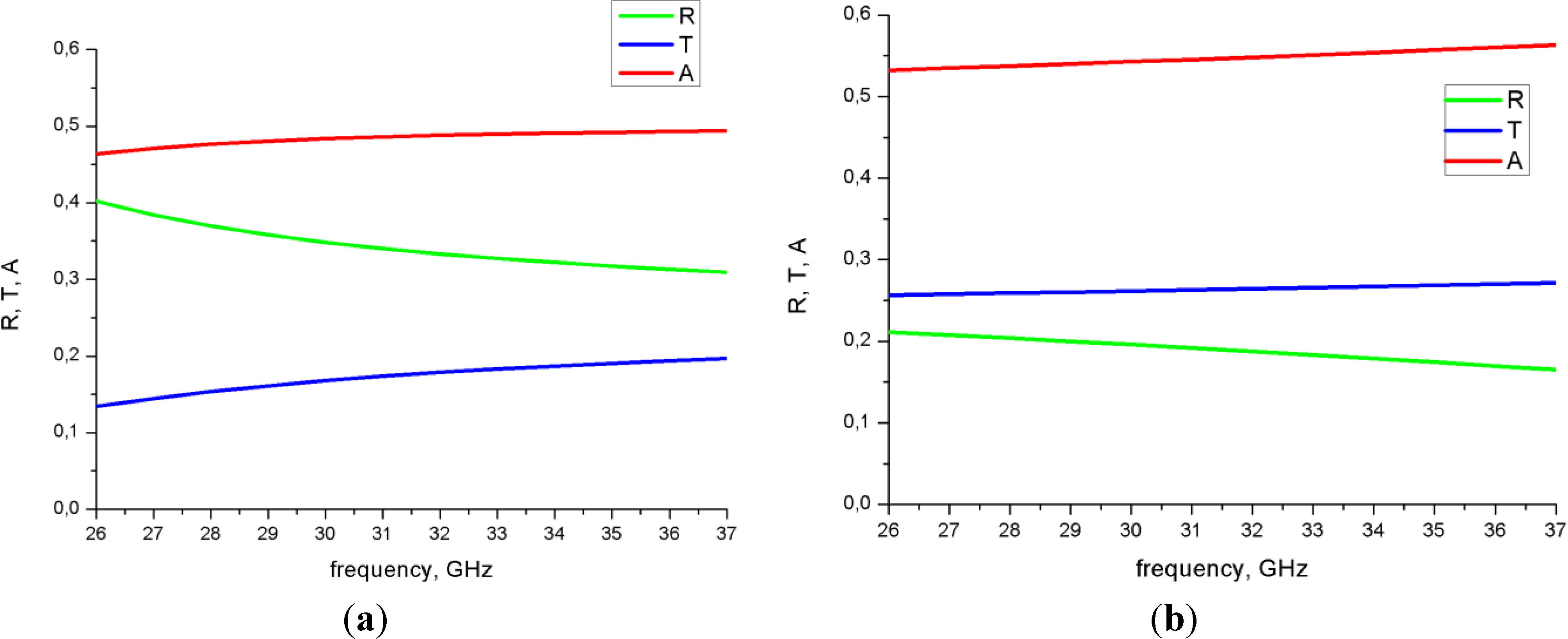
The performed waveguide measurements with 110 nm thick film revealed (see
Figure 3) that increase of frequency from 26 GHz to 37 GHz results in increasing of transmittance from 15% to 25% which is accompanied by decreasing of reflectivity. Similarly in “quartz + PyC” geometry, 30 nm thick PyC film (see
Table 2) reflects 20% of EM energy at 26 GHz and only 13% at 36 GHz. The observed frequency dispersion of transmittance and reflectance is due to the dependence of the effective incidence angle on frequency, cos
θeff =
cK0 / ω =
![Applsci 04 00255 i015]()
. This is confirmed by numerical simulation of EM wave interaction with a free standing PyC film in waveguide (see
Figure 4a). It is worth noting, however, that in free space, numerical simulation of reflectance and transmittance at normal incidence for PyC film deposited on quartz substrate revealed almost no frequency dependence (see
Figure 4b). This is because in contrast to the waveguide propagation, the characteristic interaction length in free space
lσ =
![Applsci 04 00255 i007]()
is frequency independent. Therefore in free space, the frequency dispersion can only originate from the interference caused by multiple reflections on the substrate boundaries. Since in our experiment, the substrate thickness (0.5 mm) is much smaller than the wavelength (about 1 cm), this interference can hardly influence reflectance, absorbance and transmittance that show a weak frequency dependence (
Figure 4b).
Along with conductivity and thickness, roughness can also influence the EM response of the thin film. It could be the case when both thickness and roughness are compatible with the skin depth. However one can see from
Table 1 that in our experiment, both film thickness and moreover average roughness (1.25 nm for the thickest film) were much smaller than the skin depth of PyC in the K
a-band. Thus conductivity is the major parameter that influences the absorption and transmission of the studied PyC. This fact is confirmed by excellent coincidence of experimental and numerical results shown in
Figure 3 and
Table 2. Specifically, all experimental data in whole K
a-band is described by the only parameter, conductivity σ = 4.5 × 10
14 s
−1 (5.0 × 10
4 S/m), taken from the experimental data [
6].
Figure 4.
Frequency dependence of the reflectance, transmittance and absorbance calculated for free standing (a), and deposited on the back of the 0.5 mm thick quartz substrate (b), PyC film with a thickness of 110 nm.
Figure 4.
Frequency dependence of the reflectance, transmittance and absorbance calculated for free standing (a), and deposited on the back of the 0.5 mm thick quartz substrate (b), PyC film with a thickness of 110 nm.


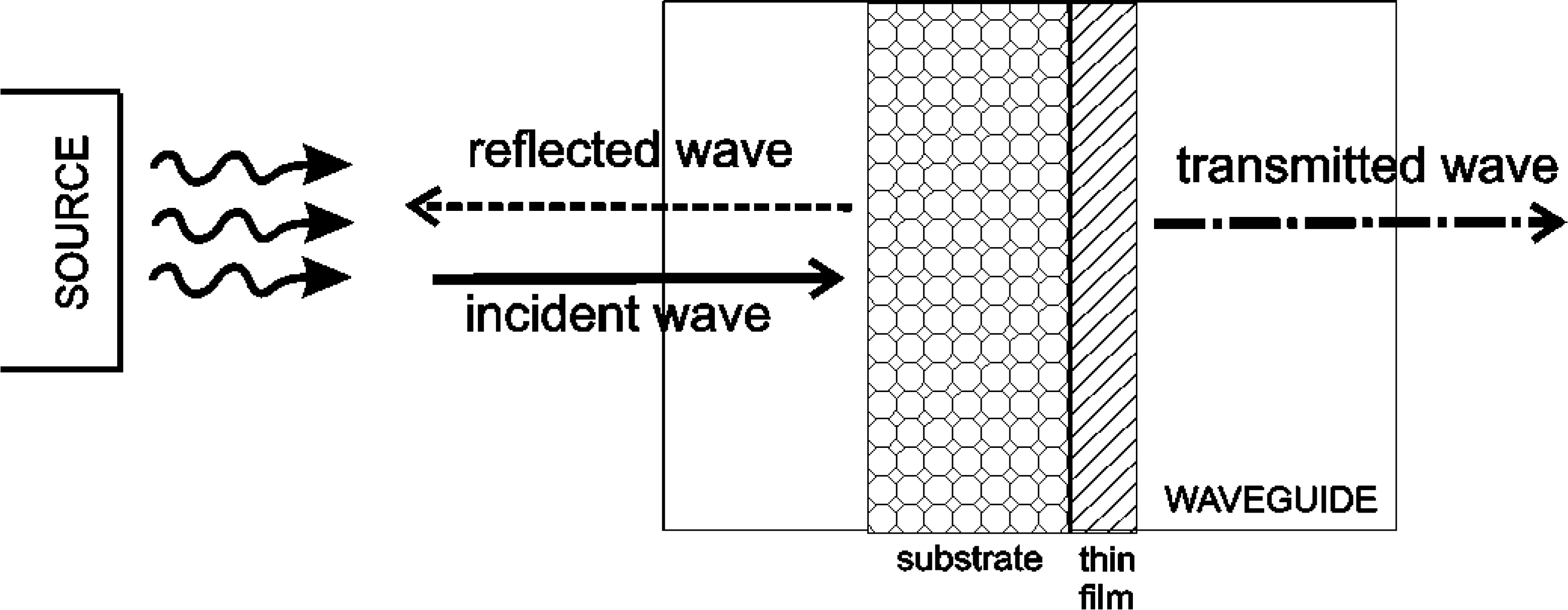
 , T =
, T =  , A = 1 – R − T. The scheme of waveguide measurements is presented in Figure 2.

 , ky =
  , where a, b are the lateral waveguide dimensions, n, m are integers, Ki =
  is the longitudinal wavenumber in the i-th medium, bi is mode amplitudes in i-th medium to be found from boundary conditions. In particular, if the waveguide supports TE1,0 mode, n = 1, m = 0 and Ki =
  .
.
 ) and reflection (r =
  ) coefficients in the “quartz + PyC” geometry:


 . This is confirmed by numerical simulation of EM wave interaction with a free standing PyC film in waveguide (see Figure 4a). It is worth noting, however, that in free space, numerical simulation of reflectance and transmittance at normal incidence for PyC film deposited on quartz substrate revealed almost no frequency dependence (see Figure 4b). This is because in contrast to the waveguide propagation, the characteristic interaction length in free space lσ =
  is frequency independent. Therefore in free space, the frequency dispersion can only originate from the interference caused by multiple reflections on the substrate boundaries. Since in our experiment, the substrate thickness (0.5 mm) is much smaller than the wavelength (about 1 cm), this interference can hardly influence reflectance, absorbance and transmittance that show a weak frequency dependence (Figure 4b).