Article

Enhancement and Reduction of Nonradiative Decay Process in Organic Light-Emitting Diodes by Gold Nanoparticles

1
Department of Electrical Engineering, National Sun Yat-Sen University, Kaohsiung 80424, Taiwan
2
Department of Electronic Engineering, Fortune Institute of Technology, Kaohsiung 83160, Taiwan
3
Department of Electrical Engineering, Kao-Yuan University, Kaohsiung 82151, Taiwan
4
Department of Applied Physics, National University of Kaohsiung, Kaohsiung 81148, Taiwan
*
Author to whom correspondence should be addressed.
Appl. Sci. 2016, 6(12), 441; https://doi.org/10.3390/app6120441
Submission received: 19 September 2016 / Revised: 30 November 2016 / Accepted: 8 December 2016 / Published: 16 December 2016

Abstract

:
The influences of gold nanoparticles (GNPs) and the buffer layer on the performance of organic light-emitting diodes are investigated in this study. The GNPs are doped into poly (3,4-ethylenedioxythiophene)-poly(styrenesulfonate) (PEDOT:PSS) and the buffer layer is introduced between the hole-transport layer and emitting layer. The GNPs are found to have the surface plasmon resonance at a wavelength of 530 nm when the mean particle size of the GNPs is 10 nm. The current efficiency of the device, at a current density of 145 mA/cm2, with GNPs and a buffer layer of 6 nm is about 1.93 times higher than that of the device with prime PEDOT:PSS because the GNPs will generate the surface plasmon resonance effect in the device and the buffer layer can considerably decrease the quenching of the fluorescence.

1. Introduction

Organic light-emitting diodes (OLEDs) possess distinctive advantages. Therefore, OLEDs presented remarkable potential in application in displays and lighting sources. Thus far, the characteristics for the device still have room to improve. Therefore, in order to optimize the efficiency of the devices, a variety of methods have been presented. The following are some examples: doping phosphorescence material into the emitting layer to enhance the performance of the device [1,2,3], improving the balance between holes and electrons within the recombination zone of the excitons [4,5,6,7], or increasing the efficiency of light extraction by decreasing the waveguide effect on the edge of the glass [8,9]. These methods can enhance the performances of OLEDs, but these methods also increased the production complexity of OLEDs.
Recently, the application of metal nanoparticles to OLEDs and inorganic light-emitting diodes has attracted considerable interest because of their unusual surface plasmon resonance effect (SPRE). It is well known that the SPRE was induced by the interaction between the surface charge of the metal and the electromagnetic field of the incident light [10,11,12,13,14,15,16]. In addition, when the metal nanoparticles are close to the fluorescent molecule, the luminous efficiency of the fluorescent molecules can be greatly increased by a decrease in the decay time of the excitons for the devices [17]. Nevertheless, when the distance is much smaller between the metal nanoparticles and fluorescent molecules, the nonradiative quenching of the excitons is generated. Furthermore, the nonradiative quenching of the excitons will result in the reduction of the efficiency for devices. Therefore, two competitive courses will take place in devices of SPRE: (I) a decrease in the efficiency of the device by nonradiative quenching of the excitons; and (II) an increase in the efficiency of the device by a reduction of the decay time of the excitons. In short, the distances between the metal nanoparticles and the fluorescent molecules are extremely important parameters in devices of SPRE.
The GNPs were doped into hole-transport layer (HTL), resulting in an increase in the efficiency of the device [18], but the causes of enhancement and quenching for fluorescence at different distances between the GNPs and the emitting layer were not described in detail. In this paper, the distance between the GNPs and the emitting layer has been optimized for enhancement of the maximum luminescence. In addition, how the distances between the GNPs and the emitting layer influenced the efficiency of the devices was also observed. Furthermore, mechanisms of increase in the radiative intensity and nonradiative quenching have been described in detail.

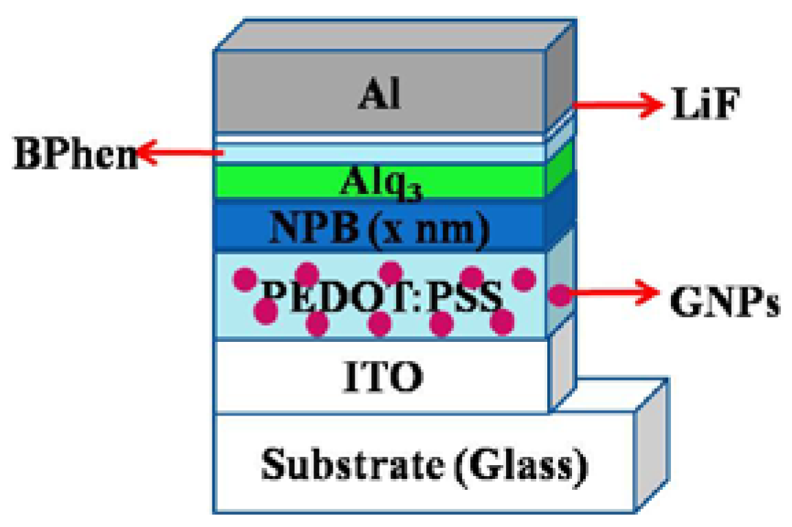
2. Experimental Section

Figure 1 presents the schematic structure of the device with GNPs and the buffer layer. Indium tin oxide (ITO) coated on glass (Uni-onward Corp., New Taipei, Taiwan) with a sheet resistance of 10 Ω/sq was used as the starting substrate. Acetone, methanol and deionized water (Uni-onward Corp., New Taipei, Taiwan) were used to clean the substrate. Afterwards, nitrogen gas (Kaohsiung, Taiwan) was used to dry it. As reported earlier [19,20], the GNPs were prepared via the electrochemical method. GNPs were dispersed into the aqueous solution of PEDOT:PSS in an optimized ration as a HTL. The resulting solution was spin-coated on ITO glass substrate, and the film thickness of PEDOT:PSS was estimated to be about 100 nm.
Afterwards, the substrates were loaded into a thermal evaporator (Junsun Tech Co. LTD., New Taipei, Taiwan). Subsequently, N,N′-Bis-(naphthalene-1-yl)-N,N′-bis(phenyl)-benzidine (NPB; x nm, 99.5%, Aldrich, Kaohsiung, Taiwan), tris-(8-hydroxyquinoline) aluminum (Alq3; 40 nm, 99.5%, Aldrich, Kaohsiung, Taiwan), 4,7-dipheny1-1, 10-phenanthroline (BPhen; 10 nm, 99.5%, Aldrich, Kaohsiung, Taiwan), lithium fluoride (LiF; 0.5 nm, 99.99%, Aldrich, Kaohsiung, Taiwan), and aluminum (Al; 100 nm, Gredmann, Taipei, Taiwan) were deposited. NPB were used as the buffer layer, while BPhen were used as the electron transport layers. Alq3 was used as an emitting layer. LiF, Al and ITO were used as electron-injection layer, cathode and anode, respectively. During the deposition, the base pressure of the chamber was maintained as low as 2.4 × 10⁻⁶ Torr. The active area of the device was 6 × 6 mm2. The deposition rates of all organic materials were maintained at 0.01 nm/s, except for the Al with deposition rate of 0.5 nm/s. Via a quartz-crystal monitor, the thickness of the layer is controlled. With a Keithley 2400 (Keithley instruments Inc., Cleveland, AL, USA), the current density-voltage (J-V) characteristics of the devices were measured, while with a PR-655 (Photo Research Inc., Syracuse, NY, USA), luminance-voltage (L-V) characteristics of the devices were measured. The absorption spectra were measured by using a U-3900 spectrophotometer (Hitachi, Tokyo, Japan). The photoluminescence (PL) spectrum and transmission electron microscope (TEM) images were measured by using an IK series (Kimmon Koha, Tokyo, Japan) and a TEM-3010 (JEOL, Tokyo, Japan), respectively. All of these measurements were conducted at room temperatures under air ambient.

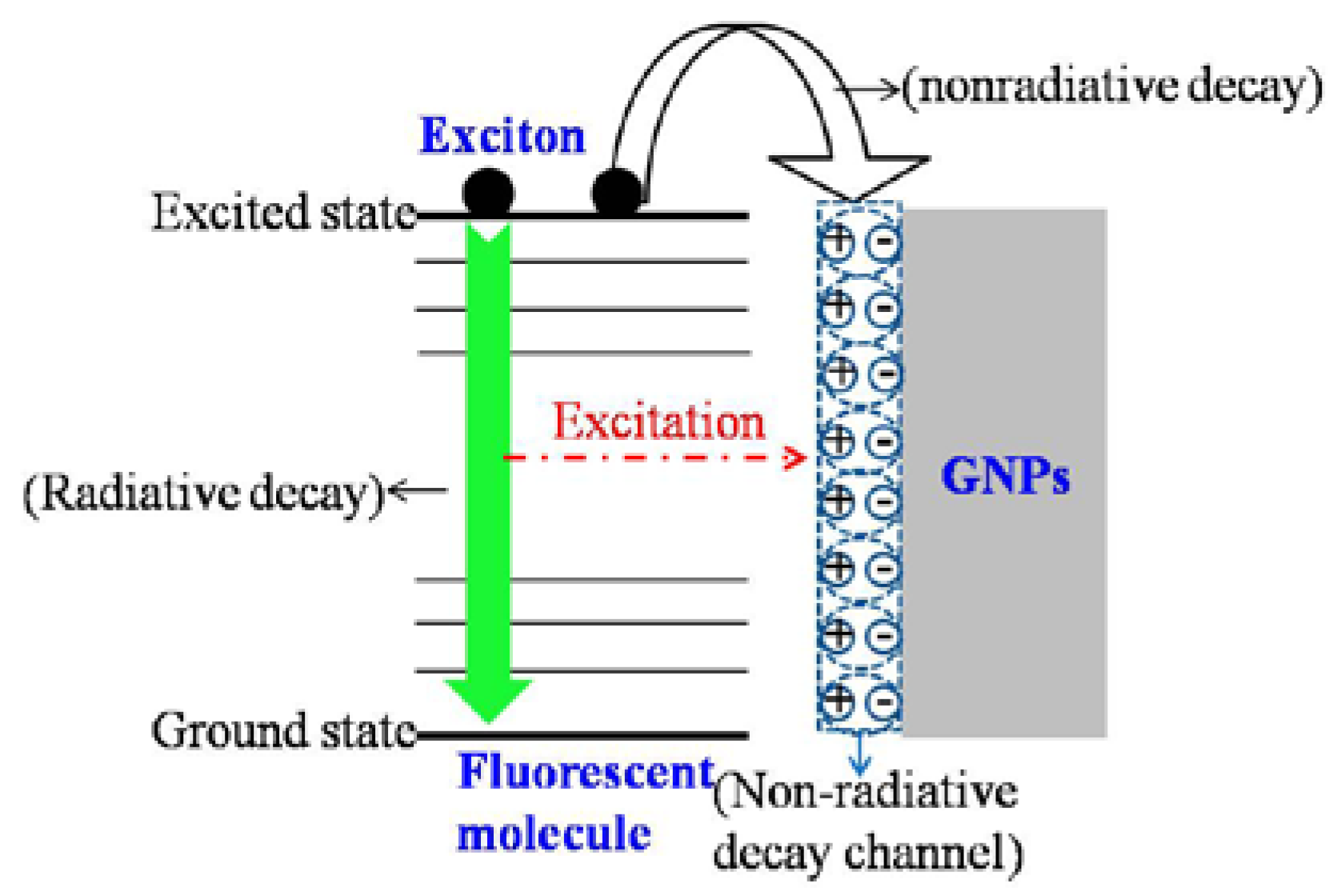
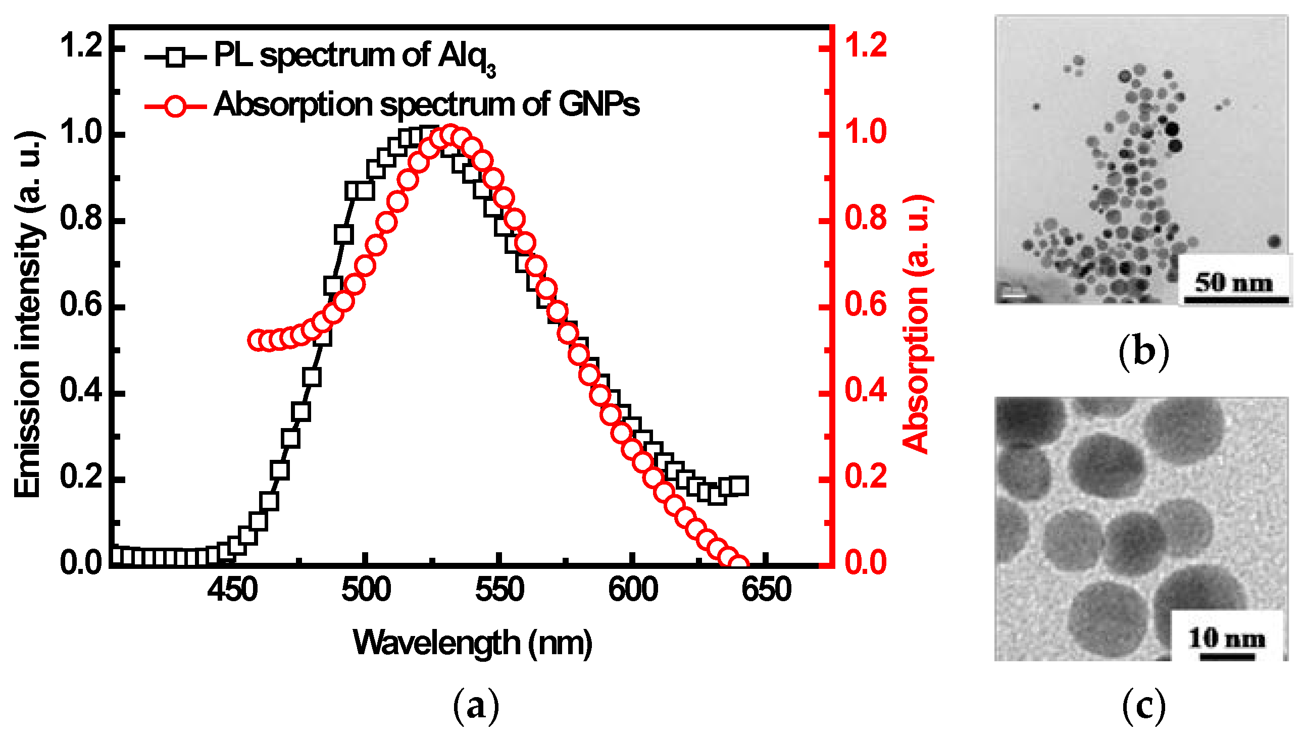
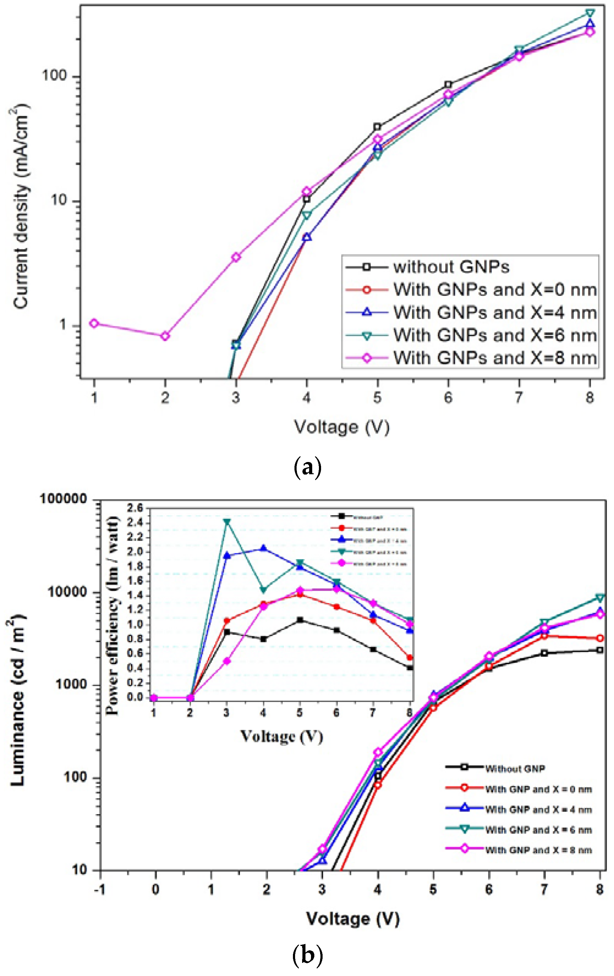
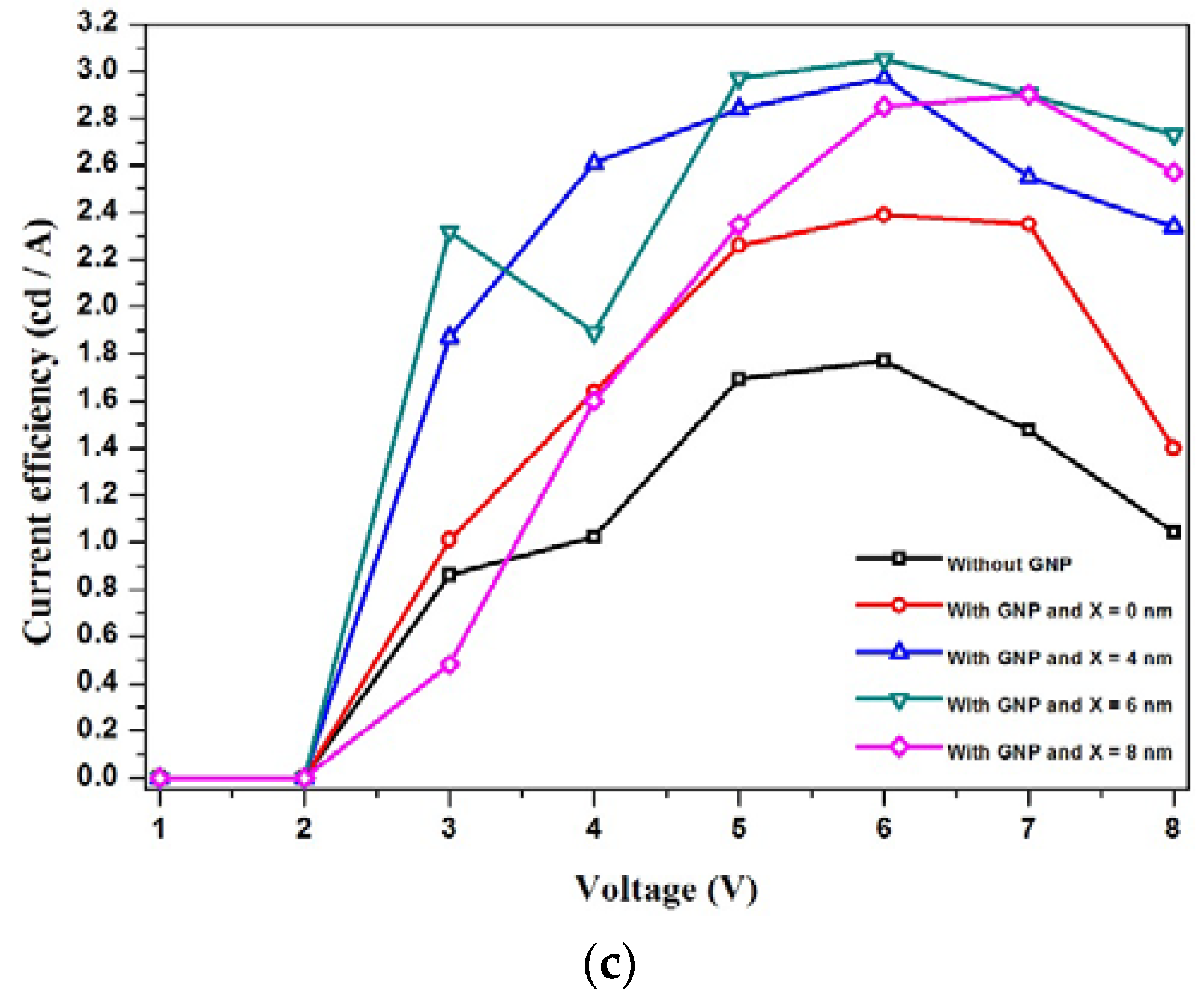
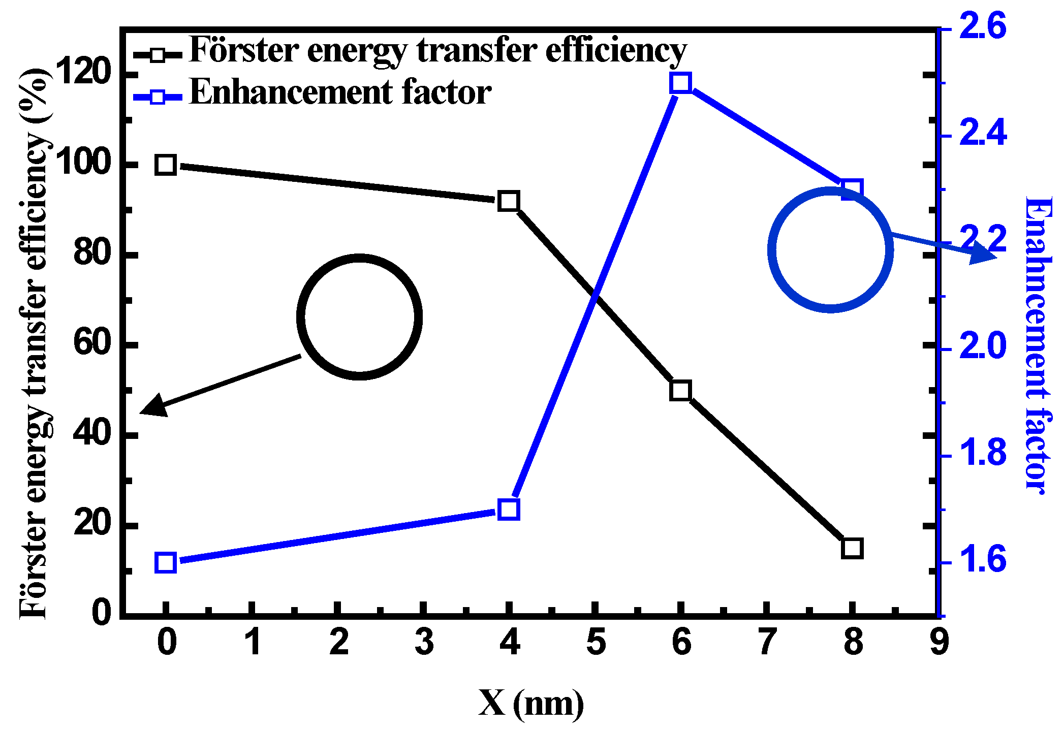
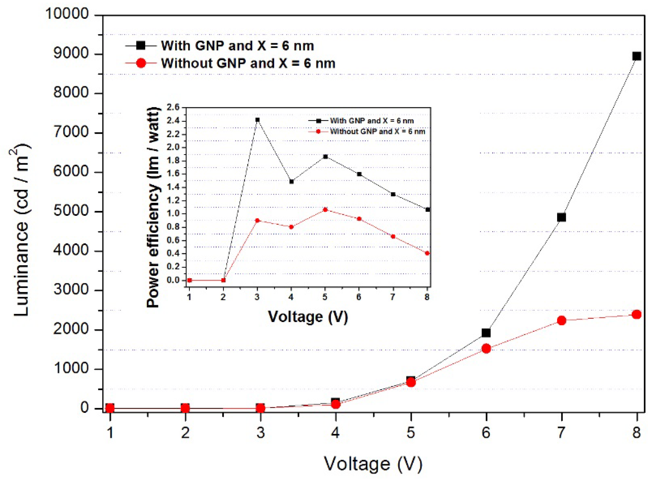
3. Results and Discussion

The absorption spectrum of GNPs and the PL spectrum of Alq3 are shown in Figure 2a. It is observed that the PL peak of Alq3 and the absorption peak of GNPs are about 523 nm and 530 nm, respectively. The GNPs can enhance the characteristics of the device when the absorption peak of GNPs is very close to the PL peak of Alq3 because of its SPRE [21]. In addition, Figure 2b,c show the TEM and high-resolution TEM images of GNPs, respectively. According to the normal and high-resolution TEM image in Figure 2b,c, the GNPs are mostly spherical and irregular in shape. Furthermore, it is also observed that the mean particle size of the GNPs in Figure 2b,c is calculated and found to be 10 nm when the absorption peak of the GNPs is 530 nm. It is well known that the absorption peak depends on the GNPs’ size, shape, and the spacing between the GNPs [22].
Because the distance between the GNPs and excitons is an extremely important parameter, the distance was tuned by changing the thickness of the buffer layer to further confirm the relationship for coupling between the surface plasmon and excitons. The resulting J-V curves of the devices without GNPs and with different spacing distances between the emissions layer (EML) and GNPs are plotted in Figure 3a. It can be clearly seen that the J-V curves of devices with GNPs and without GNPs are almost identical. The almost identical phenomenon of the current density suggests that the GNPs doped into PEDOT:PSS do not affect the hole-injection characteristics. Figure 3b shows the L-V characteristics of the device without GNPs and with different spacing distances between EML and GNPs. It is observed that the luminance of the devices with GNPs is higher than that of the device without GNPs because of the SPRE of GNPs. Furthermore, the SPRE of GNPs will result in the surface plasmon–enhanced spontaneous emission rate. The luminance of the device with GNPs at a spacing distance of 6 nm is higher than that of devices without GNPs and with the other spacing distances because the GNPs at a spacing distance of 6 nm can considerably decrease the quenching of the fluorescence. The current efficiency-voltage characteristics of devices with a buffer layer of 6 nm and without GNPs are plotted in the inset of Figure 3b. Obviously, the current efficiency of the device with a buffer layer of 6 nm is significantly higher than that of the device without GNPs because the device with a buffer layer of 6 nm not only enhanced the spontaneous recombination of the excitons but also decreased the nonradiative decay process of the excitons. However, the power efficiency of the device with a buffer layer of 6 nm is 2.43 lm/watt at 3 V.
Figure 4 shows the plot of the enhancement factor and the Förster energy transfer efficiency as a function of the spacing distance. The enhancement factor is expressed as L2/L1, where L2 is the maximum luminance of the device with GNPs and L1 is the maximum luminance of the device without GNPs. It is observed that the enhancement factors are decreased with an increase in the thickness of the spacing layer in the condition of a thickness of spacing ≥6 nm because the GNPs are close to the excitons of the EML. Furthermore, the surface plasmon–enhanced spontaneous emission rate of the device is increased when the GNPs are close to the excitons of the EML. The enhancement factors are increased with an increase in the thickness of the spacing layer in the condition of a thickness of spacing ≤6 nm because the Förster energy transfer efficiency is decreased with an increase in thickness of the spacing layer. Moreover, the nonradiative decay of excitons is decreased when the thickness of the spacing between the EML and the GNPs is increased. In addition, the maximum enhancement factor is obtained when the Förster energy transfer efficiency is 50%. The relationship between the Förster energy transfer efficiency and the spacing distance can be expressed as follows [23]:
E = 1 1 + ( R R 0 ) 6
Where the E is the Förster energy transfer efficiency, R is the spacing distance between the EML and GNPs, and R0 is the Förster radius. The Förster energy transfer efficiency of can be obtained when the spacing distance between the EML and GNPs is equal to the Förster radius. The Förster radius can be expressed as follows [24,25,26]:
R 0 = 0.0211 ( φ 0 n 4 J k 2 ) 1 6
where R0 is the Förster radius, φ 0 is the quantum yield of the donor, n is the refractive index of the medium, J is the normalized overlap integral of the donor and the acceptor spectra, and k is the orientation of the dipoles. We have investigated the values for the variables in Equation (2). Both the φ 0 and the J are 0.22 and 1.16 × 10¹⁶, respectively, with an n of 1.35 and k2 of 0.667 to calculate the optimized value of R0. Therefore, the Förster radius is calculated as 6 nm by using Equation (2). Furthermore, the enhancement factor of the device with a thickness of spacing ≤4 nm is quite low because the Förster energy transfer efficiency of devices with a thickness of spacing ≤4 nm is nearly 100%.
According to the relative studies [27], which are clearly researched for the important role of the buffer layer, the nonradiative decay process of the excitons in the device can be avoided by the addition of the NPB between the hole-transport layer and the emitting layer. We also find that the power efficiency of the device with the NPB buffer layer is higher than that of the device without the NPB buffer layer. At the same time, the devices with and without GNPs have a significant difference in luminance characteristics under different applied voltages [27]. In order to further research how strong the influence of the GNPs is, we conducted a proper comparison with pure PEDOT:PSS and NPB at the optimized thickness of 6 nm in Figure 5. Both Figure 5 and its inserted image show the difference with GNPs in the PEDOT:PSS layer and without by the luminance-voltage and power efficiencies–voltage curves, respectively. It is clear that the device with GNPs has higher luminance and power efficiencies than that of device without GNPs. When the applied voltage is below 5 V, the results for the luminance of the device under two conditions are not different. Additionally, there is a slight increase of the luminance of the device when we enhance the applied voltage from 5 to 6 V. Finally, we have found a surprising consequence that the luminance of the device is largely increased when the voltage reaches more than 6 V. In the insert in Figure 5, the results show that the device with GNPs is excellent for power efficiency. According to the investigation of polymer effects by time-resolved PL [28,29], at the same time, the decay rate from the nonradiative process of excitons is about 4 ns, which is same as the result of doped Alq3 organic semiconductors. We also find that there is a decrease of the power efficiency for both of them when the applied voltage is increased from 3 to 4 V. The power efficiency is slightly increased when the applied voltage reaches 5 V, although there is a downward trend from 5 to 8 V. The decreasing trend would be linear if we ensured that the charge transport problem is normally main factor. Thus, the improved performance is attributed to the strong influence of the SPRE.
Figure 6 shows the schematic diagram of the nonradiative decay process of excitons. The excitation of the surface plasmon polariton modes results in the nonradiative decay process of excitons, which propagate along the surface of the GNPs. Furthermore, the extra nonradiative decay channel at the interface between the fluorescent molecule and the GNPs results from the excitation of the surface plasmon polariton modes [30]. Therefore, the enhancement factor of the device with GNPs will be decreased when the GNPs are close to the excitons of the EML. Moreover, the extra nonradiative decay channel at the interface between the fluorescent molecule and the GNPs will be generated when the GNPs are close to the excitons of the EML.

4. Conclusions

In summary, the GNPs are doped into PEDOT:PSS and the buffer layer is introduced between the hole-transport layer and emitting layer. The maximum luminance of the device with GNPs is higher than that of device without GNPs because of the SPRE of GNPs. Furthermore, the SPRE of GNPs results in the surface plasmon–enhanced spontaneous emission rate. In addition, the best performance is obtained when the spacing distance between the GNPs and the EML is equal to the Förster radius. Furthermore, the current efficiency of the device, at a current density of 145 mA/cm2, with GNPs and a buffer layer of 6 nm is about 1.93 times higher than that of the device with prime PEDOT:PSS because the GNPs at a spacing distance of 6 nm not only enhanced the spontaneous recombination of the excitons but also decreased the nonradiative decay process of the excitons.

Acknowledgments

This work was partially supported by the Ministry of Science and Technology of Taiwan under Contract No. MOST 105-2221-E-390-027.

Author Contributions

Chia-Yuan Gao and Chien-Jung Huang analyzed the materials; Chia-Yuan Gao, Kan-Lin Chen, Po-Wen Sze, Ying-Chung Chen and Chien-Jung Huang conceived and designed the experiments; Chia-Yuan Gao performed the experiments; Chia-Yuan Gao and Chien-Jung Huang analyzed the data; Kan-Lin Chen, Po-Wen Sze, Ying-Chung Chen and Chien-Jung Huang contributed analysis tools; Chia-Yuan Gao write the paper.

Conflicts of Interest

The authors declare no conflict of interest.

References

  1. Lee, S.J.; Seo, J.H.; Kim, J.H.; Kim, H.M.; Lee, K.H.; Yoon, S.S.; Kim, Y.K. Efficient triplet exciton confinement of white organic light-emitting diodes using a heavily doped phosphorescent blue emitter. Thin Solid Film 2010, 518, 6184–6187. [Google Scholar] [CrossRef]
  2. Zhang, Y.; Slootsky, M.; Forrest, S.R. Enhanced efficiency in high-brightness fluorescent organic light emitting diodes through triplet management. Appl. Phys. Lett. 2011, 99, 223303. [Google Scholar] [CrossRef]
  3. Xie, C.Y.G.; Murawski, C.; Lee, J.; Ventsch, F.; Leo, K.; Gather, M.C. Understanding the influence of doping in efficient phosphorescent organic light-emitting diodes with an organic p–i–n homojunction. Org. Electron. 2013, 14, 1695–1703. [Google Scholar]
  4. Xhao, Y.; Duan, L.; Zhang, D.; Hou, L.; Qiao, J.; Wang, L.; Qiu, Y. Small molecular phosphorescent organic light-emitting diodes using a spin-coated hole blocking layer. Appl. Phys. Lett. 2012, 100, 083304. [Google Scholar]
  5. Narayan, K.; Varadarajaperumal, S.; Rao, G.M.; Varma, M.M.; Srinivas, T. Effect of thickness variation of hole injection and hole blocking layers on the performance of fluorescent green organic light emitting diodes. Curr. Appl. Phys. 2013, 13, 18–25. [Google Scholar] [CrossRef]
  6. Park, Y.W.; Choi, J.H.; Park, T.H.; Song, E.H.; Kim, H.; Lee, H.J.; Shin, S.J.; Ju, B.-K.; Song, W.J. Barrierless hole injection through sub-bandgap occupied states in organic light emitting diodes using substoichiometric MoOx anode interfacial layer. Appl. Phys. Lett. 2012, 100, 013312. [Google Scholar]
  7. Kim, K.; Hong, K.; Lee, I.; Kim, S.; Lee, J.-L. Electron injection in magnesium-doped organic light-emitting diodes. Appl. Phys. Lett. 2012, 101, 141102. [Google Scholar] [CrossRef]
  8. Sun, Y.; Foorrest, S.R. Enhanced light out-coupling of organic light-emitting devices using embedded low-index grids. Nat. Photon. 2008, 2, 483–487. [Google Scholar] [CrossRef]
  9. Koh, T.W.; Choi, J.M.; Lee, S.; Yoo, S. Optical Outcoupling Enhancement in Organic Light-Emitting Diodes: Highly Conductive Polymer as a Low-Index Layer on Microstructured ITO Electrodes. Adv. Mater. 2010, 22, 1849–1853. [Google Scholar] [CrossRef] [PubMed]
  10. WBarnes, L.; Dereux, A.; Ebbesen, T.W. Surface plasmon subwavelength optics. Nature 2003, 424, 824–830. [Google Scholar] [CrossRef] [PubMed]
  11. Kumar, A.; Tyagi1, P.; Srivastava1, R.; Mehta, D.S.; Kamalasanan, M.N. Energy transfer process between exciton and surface plasmon: Complete transition from Forster to surface energy transfer. Appl. Phys. Lett. 2013, 102, 203304. [Google Scholar] [CrossRef]
  12. Kumar, A.; Srivastava, R.; Tyagi, P.; Mehta, D.S.; Kamalasanan, M.N. Efficiency enhancement of organic light emitting diode via surface energy transfer between exciton and surface plasmon. Org. Electron. 2012, 13, 159–165. [Google Scholar] [CrossRef]
  13. Kim, T.; Kang, H.; Jeong, S.; Kang, D.J.; Lee, C.; Lee, C.H.; Seo, M.K.; Lee, J.Y.; Kim, B.J. Au@ Polymer Core–Shell Nanoparticles for Simultaneously Enhancing Efficiency and Ambient Stability of Organic Optoelectronic Devices. ACS Appl. Mater. Interfaces 2014, 6, 16956–16965. [Google Scholar] [CrossRef] [PubMed]
  14. Kumar, A.; Srivastava, R.; Mehta, D.S.; Kamalasanan, M.N. Surface plasmon enhanced blue organic light emitting diode with nearly 100% fluorescence efficiency. Org. Electron. 2012, 13, 1750–1755. [Google Scholar] [CrossRef]
  15. Choi, H.; Ko, S.J.; Choi, Y.; Joo, P.; Kim, T.; Lee, B.R.; Jung, J.W.; Choi, H.J.; Cha, M.; Jeong, J.R.; et al. Status and prospects for ternary organic photovoltaics. Nat. Photonics 2015, 9, 491–500. [Google Scholar]
  16. Kim, D.H.; Kim, T.W. Enhancement of the current efficiency of organic light-emitting devices due to the surface plasmonic resonance effect of dodecanethilol-functionalized Au nanoparticles. Org. Electron. 2016, 34, 262–266. [Google Scholar] [CrossRef]
  17. Chen, Y.C.; Gao, C.Y.; Chen, K.L.; Meen, T.H.; Huang, C.J. Enhancement and Quenching of Fluorescence by Silver Nanoparticles in Organic Light-Emitting Diodes. J. Nanomater. 2013, 2013, 841436. [Google Scholar] [CrossRef]
  18. Xiao, Y.; Yang, J.P.; Cheng, P.P.; Zhu, J.J.; Xu, Z.Q.; Deng, Y.H.; Lee, S.T.; Li, Y.Q.; Tang, J.X. Surface plasmon-enhanced electroluminescence in organic light-emitting diodes incorporating Au nanoparticles. Appl. Phys. Lett. 2012, 100, 013308. [Google Scholar] [CrossRef]
  19. Huang, C.J.; Chiu, P.H.; Wang, Y.H.; Chen, K.L.; Linn, J.J.; Yang, C.F. Electrochemically Controlling the Size of Gold Nanoparticles Electrochemical Synthesis and Engineering. J. Electrochem. Soc. 2006, 153, D193–D198. [Google Scholar] [CrossRef]
  20. Huang, C.J.; Chiu, P.H.; Wang, Y.H.; Chen, W.R.; Meen, T.H. Synthesis of the Gold Nanocubes by Electrochemical Technique Electrochemical Synthesis and Engineering. J. Electrochem. Soc. 2006, 153, D129–D133. [Google Scholar] [CrossRef]
  21. Chen, Y.C.; Gao, C.Y.; Chen, K.L.; Huang, C.J. Surface plasmon-enhanced localized electric field in organic light-emitting diodes by incorporating silver nanoclusters. Appl. Surf. Sci. 2014, 295, 266–269. [Google Scholar] [CrossRef]
  22. Gao, C.Y.; Chen, Y.C.; Chen, K.L.; Huang, C.J. Surface plasmon enhanced organic light emitting diodes by gold nanoparticles with different sizes. Appl. Surf. Sci. 2015, 356, 791–794. [Google Scholar] [CrossRef]
  23. Yun, C.S.; Javier, A.; Jennings, T.; Fisher, M.; Hira, S.; Peterson, S.; Hopkins, B.; Reich, N.O.; Strouse, G.F. Nanometal Surface Energy Transfer in Optical Rulers, Breaking the FRET Barrier. J. Am. Chem. Soc. 2005, 127, 3115–3119. [Google Scholar] [CrossRef] [PubMed]
  24. Zhang, X.; Marocico, C.A.; Lunz, M.; Gerard, V.A.; Gun’ko, Y.K.; Lesnyak, V.; Gaponik, N.; Susha, A.S.; Rogach, A.L.; Bradley, A.L. Wavelength, Concentration, and Distance Dependence of Nonradiative Energy Transfer to a Plane of Gold Nanoparticles. ACS Nano 2012, 6, 9283–9290. [Google Scholar] [CrossRef] [PubMed]
  25. Lakowicz, J.R. Principles of Fluorescence Spectroscopy; Kluwer Academic/Plenum: New York, NY, USA, 1999. [Google Scholar]
  26. Van der Meer, B.W.; Coker, G.; Chen, S.Y.S. Resonance Energy Transfer: Theory and Data; VCH: New York, NY, USA, 1994. [Google Scholar]
  27. Gao, C.Y.; Chen, Y.C.; Chen, K.L.; Huang, C.J. Double surface plasmon enhanced organic light-emitting diodesby gold nanoparticles and silver nanoclusters. Appl. Surf. Sci. 2015, 359, 749–753. [Google Scholar] [CrossRef]
  28. Feng, S.W. Dependence of the dynamics of exciton transport, energy relaxation, and localization on dopant concentration in disordered C545Tdoped Alq3 organic semiconductors. Opt. Mater. Express 2014, 4, 798–809. [Google Scholar] [CrossRef]
  29. So, F.; Kondakoc, D. Degradation Mechanisms in Small-Molecule and Polymer Organic Light-Emitting Diodes. Adv. Mater. 2010, 22, 3762–3777. [Google Scholar] [CrossRef] [PubMed]
  30. Ford, G.W.; Weber, W.H. Electromagnetic interactions of molecules with metal surfaces. Phys. Rep.-Rev. Sec. Phys. Lett. 1984, 113, 195–287. [Google Scholar] [CrossRef]
Figure 1. Schematic structure of devices with GNPs and the buffer layer.
Applsci 06 00441 g001
Figure 2. (a) Absorption spectrum of the GNPs and PL spectrum of the Alq3; (b) TEM image of the GNPs; (c) High-resolution TEM images of the GNPs.
Applsci 06 00441 g002
Figure 3. (a) Current density-voltage curves; (b) luminance-voltage curves in log scale; and (c) current efficiencies curves of devices without GNPs and with different spacing distances. Inset of (b) shows the power efficiency-voltage characteristics of device.
Applsci 06 00441 g003aApplsci 06 00441 g003b
Figure 4. Enhancement factor and Förster energy transfer efficiency for different spacing between emission layer and GNPs.
Applsci 06 00441 g004
Figure 5. Luminance-voltage curves of devices with and without GNPs when the thickness of the NPB is 6 nm and the inset figure shows the power efficiency-voltage characteristics of the device under the same conditions.
Applsci 06 00441 g005
Figure 6. Schematic diagram of nonradiative decay process.
Applsci 06 00441 g006

