Article

Detection of On-Chip Generated Weak Microwave Radiation Using Superconducting Normal-Metal SET

by
Behdad Jalali-Jafari
1,2,*,
Sergey V. Lotkhov
1 and
Alexander B. Zorin
1
1
Physikalisch-Technische Bundesanstalt, Bundesallee 100, Braunschweig 38116, Germany
2
Department of Microtechnology and Nanoscience (MC2), Chalmers University of Technology, Göteborg SE-412 96, Sweden
*
Author to whom correspondence should be addressed.
Appl. Sci. 2016, 6(2), 35; https://doi.org/10.3390/app6020035
Submission received: 30 November 2015 / Revised: 13 January 2016 / Accepted: 19 January 2016 / Published: 27 January 2016
(This article belongs to the Special Issue Applied Single-Electron Transistors)

Abstract

:
The present work addresses quantum interaction phenomena of microwave radiation with a single-electron tunneling system. For this study, an integrated circuit is implemented, combining on the same chip a Josephson junction (Al/AlO x /Al) oscillator and a single-electron transistor (SET) with the superconducting island (Al) and normal-conducting leads (AuPd). The transistor is demonstrated to operate as a very sensitive photon detector, sensing down to a few tens of photons per second in the microwave frequency range around f 100 GHz. On the other hand, the Josephson oscillator, realized as a two-junction SQUID and coupled to the detector via a coplanar transmission line (Al), is shown to provide a tunable source of microwave radiation: controllable variations in power or in frequency were accompanied by significant changes in the detector output, when applying magnetic flux or adjusting the voltage across the SQUID, respectively. It was also shown that the effect of substrate-mediated phonons, generated by our microwave source, on the detector output was negligibly small.

1. Introduction

Over the past few decades, rapid progress in nanofabrication has brought up a scope of very sensitive mesoscopic superconducting circuits operating with single quanta of physical quantities. These advances are promising for applications in electrical metrology and quantum information technology, for example, in single-electron pumping [1,2,3], which is the basic mechanism for the electron-counting capacitance standard [4,5] and a quantum current standard [6]. In the superconducting qubits, single charge, single flux or single photon states interact to give rise to a variety of quantum algorithms [7,8].
For accurate operation, the single-quantum circuits must be protected from stray electromagnetic radiation (emitted, for example, by warmer parts of the cryogenic setup) down to the utmost level of single microwave photons. Unwanted photon-induced processes were found to be responsible for the deterioration of the pumping performance by many orders of magnitude: the achieved relative uncertainty of electron transfer ϵ 10 8 greatly exceeded the theoretical prediction ϵ 10 20 [9]. A similar effect was also demonstrated in studies with a hybrid single-electron turnstile [10,11]. Significant improvement has been recently reported for the retention time of a single-electron trap using a neatly designed mK-setup with double shielding of the sample space [12]. Furthermore, the radiation-induced generation of quasiparticles is considered to be an important decoherence mechanism in the superconducting qubit systems (see [13] and references therein). Therefore, studying the interaction mechanisms of quantum devices with microwave radiation and independent characterization of the microwave background of a sample at mK temperatures is of significant importance.
Single microwave photon detection and spectroscopy using small tunnel junctions have been the subject of various studies (see, e.g., [14,15,16,17,18,19]). In particular, the Coulomb blockade circuits built using S ̲ ingle E ̲ lectron T ̲ ransistors (SETs) were found to be efficient radiation detectors down to single-photon sensitivity levels in the relevant frequency range around f 100 GHz. Recently, appreciable microwave sensitivity has been envisaged for a N ̲ ormal metal– S ̲ uperconductor– N ̲ ormal metal (NISIN, “I” stands for I ̲ nsulating barrier) SET with a superconducting island [20], which we denote here as an “NISIN detector”. A remarkable advantage of this detector appears to be due to an intrinsic signal amplification effect: each photon-excited quasiparticle in the superconducting island launches a sequence of tunneling events with many (∼ 10 2 ÷ 10 3 ) electrons transferred, thus boosting the device sensitivity. Up to now, the photon-assisted tunneling manifested itself in the NISIN SET as non-vanishing tunnel currents at low bias voltages in the subgap range, V b < 2 Δ / e , where Δ is the energy gap of the superconducting island [10]. A more systematic study is, however, needed for determining the response characteristics of the detector, for which purpose weak microwave radiation with a controllable spectrum should be generated and exposed to the detector.
In the present work, we report on the radiation detection peculiarities of an NISIN detector included in a complete microwave circuit with a Josephson-junction-based microwave generator coupled to the detector via the specially designed transmission line. A clear response even to very weak microwave signals has been observed and demonstrated to be tunable both in power and frequency. A high amplification factor could be evaluated through comparison of the experimental response with the calculated rates of photon-assisted tunneling of quasiparticles into the superconducting island. The frequency dependence of the detected microwave signal was investigated experimentally using two different types of coupling element. We also evaluated a contribution of quasiparticle-recombination phonons to the output signal and found it in our circuit, being negligibly small in the frequency range of interest.

2. Experimental Section

The complete circuit including the NISIN detector, the Josephson microwave source and the coupling element was fabricated on a thermally oxidized Si substrate. The patterns of different circuit components were defined by several electron beam lithography steps. Tunnel junctions were fabricated using the standard shadow evaporation technique including an oxidation step to form the tunnel barriers [21,22]. The detailed description of our fabrication routines can be found elsewhere [18,23,24]. In the following subsections, we discuss the operation principle and introduce the parameters of the component elements used in our integrated circuit.

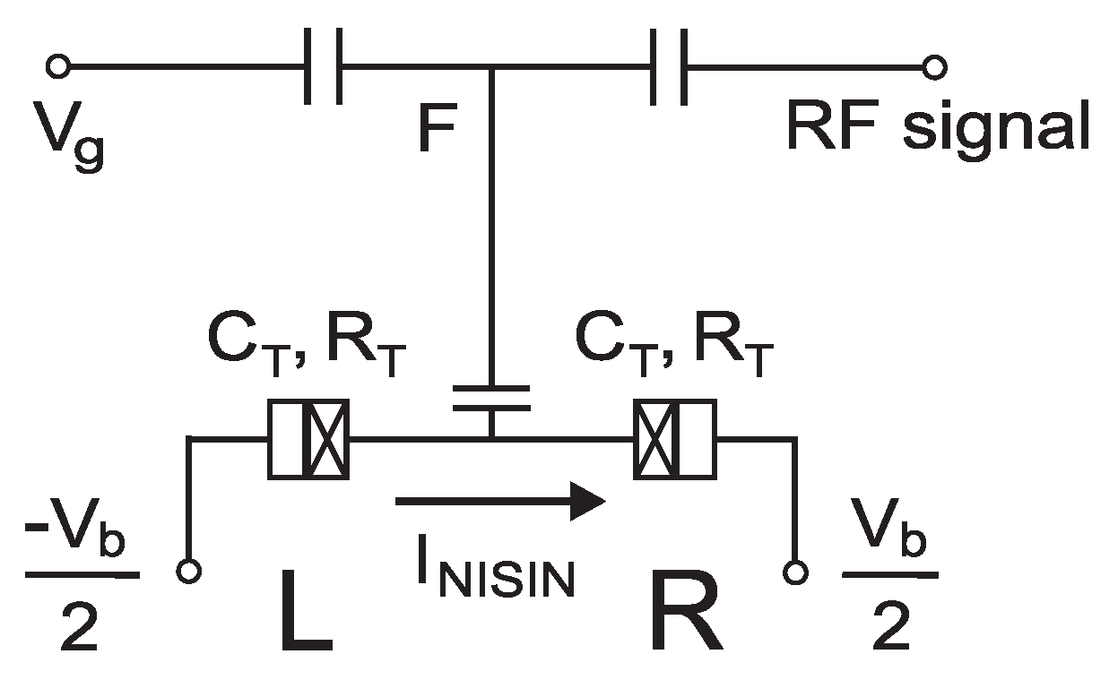
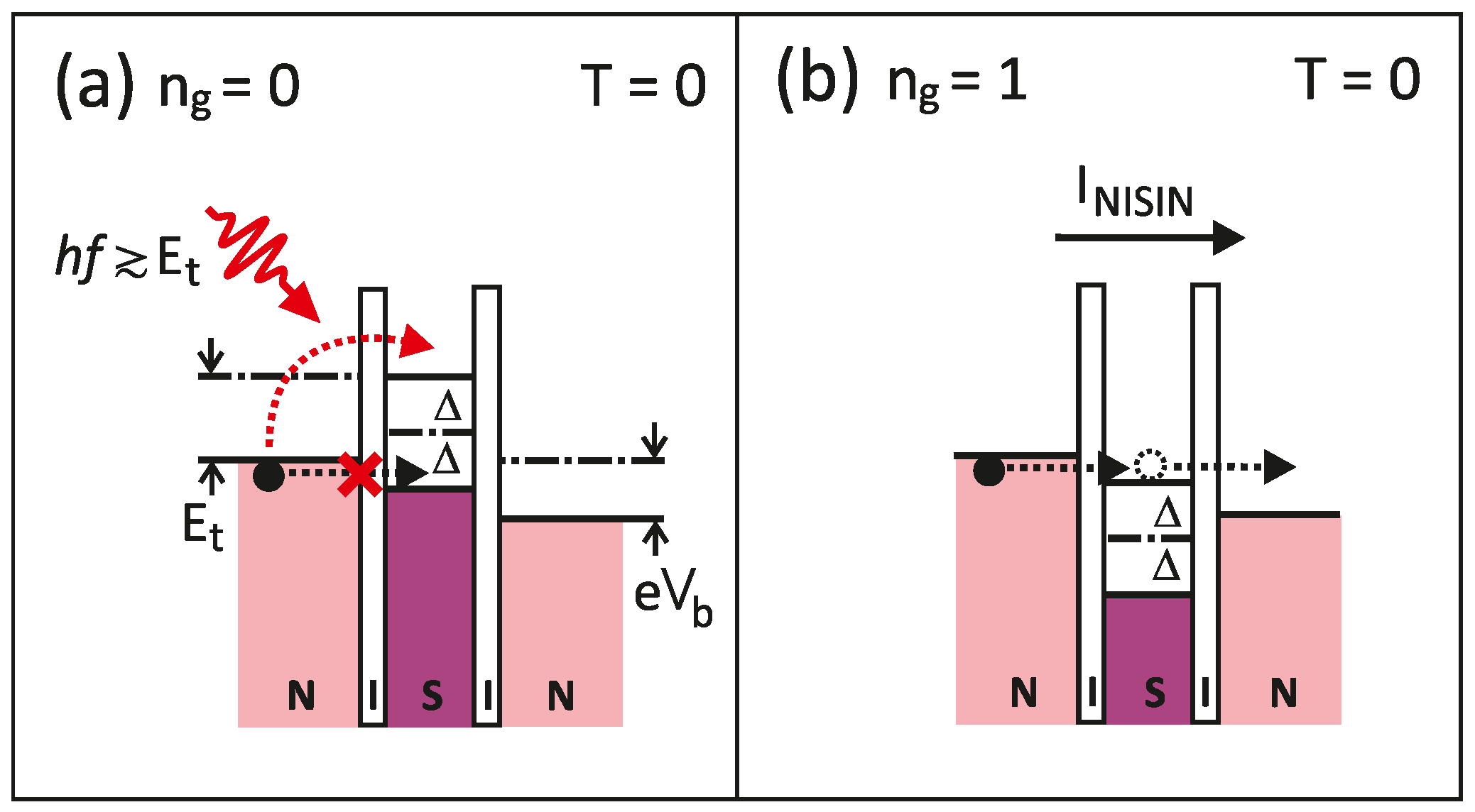
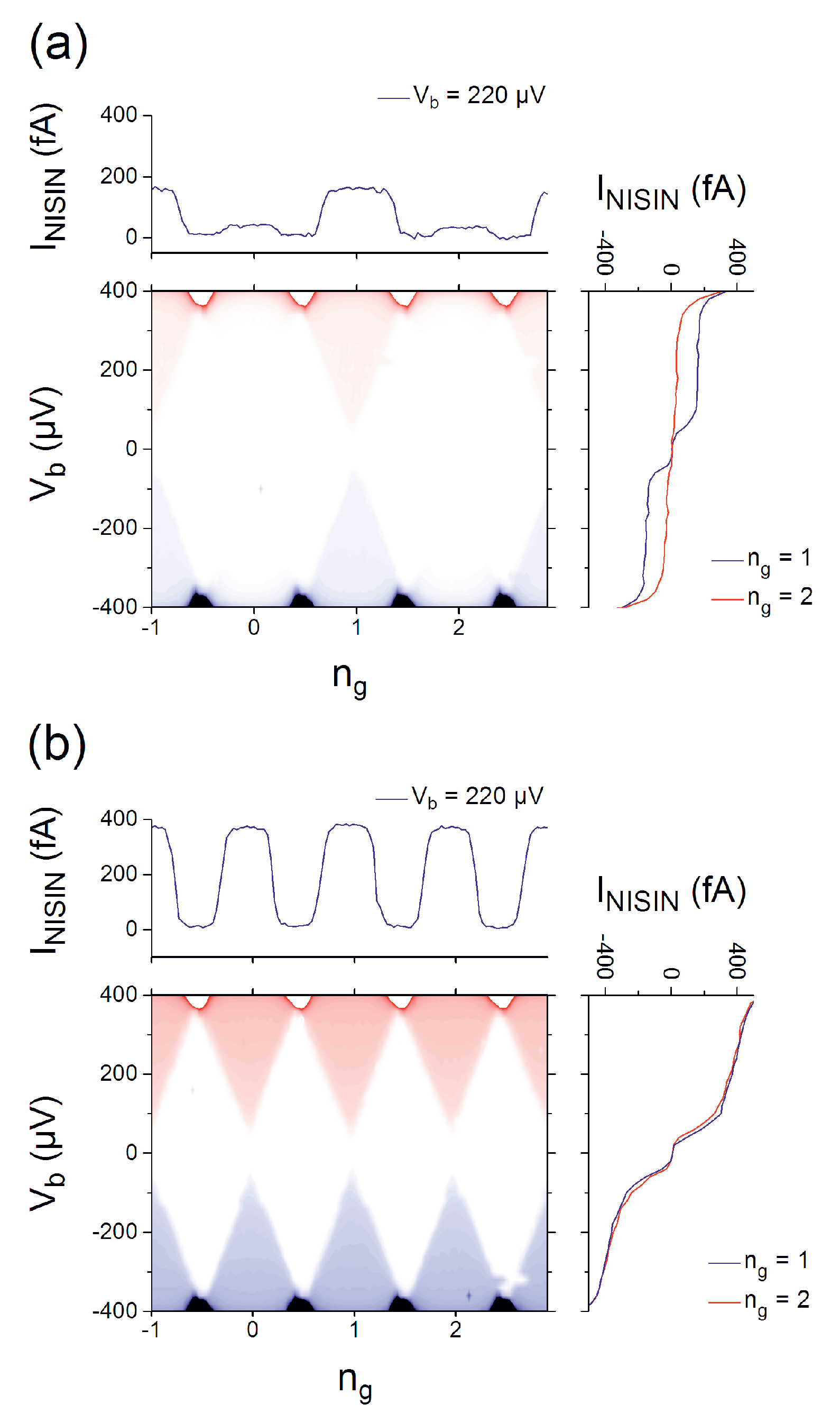
2.1. NISIN SET as a Microwave Photon Detector

The NISIN detector consists of a small superconducting island connected to two normal-metal leads via small tunnel junctions as shown schematically in Figure 1. The island is capacitively coupled through a floating gate electrode F, to a lead used for DC tuning voltage V g on one side, and to the source of the microwave signal on the other side. The DC voltage V g induces the polarization charge on the island, q g n g e = C g V g , where n g is the dimensionless gate-induced charge and C g is the effective coupling capacitance between the voltage lead and the island. The tunneling current through the device, I NISIN , is measured in a symmetric voltage-bias mode ( ± V b / 2 ) and is considered to be the detector output signal.
The charge tunneling mechanism in an NISIN transistor was investigated earlier in various regimes comprising either Andreev reflection [25,26] or single quasiparticle tunneling [20] as the dominant transport process. In the following, we briefly present the photon-activated charge transfer and signal amplification mechanism in this device. For the purpose of clarity, we address a simplified case of low temperatures, k B T Δ , where k B is the Boltzmann constant, and omit the contribution to the tunneling rates of thermally populated electron states above the Fermi level in the normal leads and thermally excited quasiparticles in the superconducting island. A more rigorous model of the tunneling current in the NISIN transistor based on a master equation approach can be found in [20].
Figure 1. Equivalent circuit of the NISIN detector. The microwave (RF) signal and the DC tuning voltage, V g , are capacitively coupled to the superconducting island through the floating gate F. NIS tunnel junctions, each with resistance R T and capacitance C T , are formed between superconducting (Al, crossed boxes) and normal conducting (AuPd, open boxes) electrodes.
Applsci 06 00035 g001
The barrier height for electron tunneling from the lead to the superconducting island depends on the island charging energy E C = e 2 / 2 C Σ ( C Σ is the total capacitance of the island including the capacitance of the junctions and the gate capacitance), superconducting gap energy Δ, and the gate and bias voltages V g and V b , respectively, and can be written as: E t = E C + Δ e V b / 2 2 E C · n g . At T = 0 , if the gate voltage is tuned to an even value of n g (e.g., n g = 0 , see the energy diagram shown in Figure 2a), an addition of one extra electron to the island requires an energy equal to at least a threshold energy E t e v e n = Δ + E C e V b / 2 . Therefore, at low bias voltages, V b < 2 ( E C + Δ ) / e , no current passes through the device and the transistor is in Coulomb blockade regime.
Figure 2. Energy diagram of the NISIN SET at zero temperature. (a) At n g = 0 and small bias voltages, the electron tunneling to the island is prohibited by the energy barrier E t , while absorption of a photon with energy E ph E t results in bringing one quasiparticle to the island (red dotted arrow); (b) When n g = 1 , the height of the tunnel barrier is reduced and applying a small bias voltage results in the finite tunneling current I NISIN .
Applsci 06 00035 g002
Changing n g to an odd integer number (e.g., n g = 1 , Figure 2b) reduces the barrier height down to the value E t o d d = Δ E C e V b / 2 and applying a small subgap bias voltage opens a possibility of a single-quasiparticle current through the island. The quasiparticle current includes a train of two-step tunneling cycles in the NISIN double junction (we assume, for simplicity, a symmetric case). In the first step, an electron tunnels from a lead into the superconducting island and occupies a free quasiparticle state. The rate of this process, Γ + E C + e V b / 2 2 Δ 2 / e 2 R T 10 10 s 1 (similar expression was used, e.g., by Averin et al. [3]), is relatively high as compared to that in the second step. The second step includes a quasiparticle escape out of the superconducting island via one of two different tunneling processes: either with or without a Cooper pair formation in the island. These two possible processes are only favorable if they involve the quasiparticle state excited in the first step and both have the same rate, Γ 10 5 s 1 Γ + . Rate Γ depends on the properties of the superconducting island and the tunneling resistance R T while being independent of the biasing conditions as shown in [20]. The current I NISIN is thus determined by the lowest effective rate, i.e., I NISIN 2 e Γ , where the factor 2 sums up the rates of both possible processes in the second step.
When the device is irradiated with photons with energy E ph = h f E t , an electron from the lead can tunnel into (Figure 2a, red dotted arrow) or out of the superconducting island (the diagram is not shown) and sum up with the induced charge n g e , thus effectively changing the gate potential V g = n g e / C g ( n g ± 1 ) e / C g . Starting from the even state, this change opens, for a short time, the single quasiparticle current channel similar to that in the odd state. The lifetime of the excited state depends on the properties of the NISIN device, in particular, on the rates of the quasiparticle escape or its recombination inside the superconducting island and greatly exceeds the inverse tunneling rate ( Γ ) 1 . This enables sequential tunneling of many electrons and, therefore, operation of the NISIN SET as a current amplifier with the gain G I NISIN / e Γ ph 1 , where Γ ph is the photon absorption rate.
Table 1 presents the parameters for one of the NISIN transistors used in our experiment including the size of the superconducting island and tunnel junctions, the junctions’ tunnel resistance R T , the island charging energy E C and the superconducting gap energy Δ.
Table 1. Typical measured values for the NISIN transistor parameters. Values of R T , E C and Δ are measured at T 15 mK.
Island AreaTunnel Area R T E C Δ
(µm 2 )( nm 2 ) (kΩ)(µeV)(µeV)
1.4 × 0.0850 × 50110140210

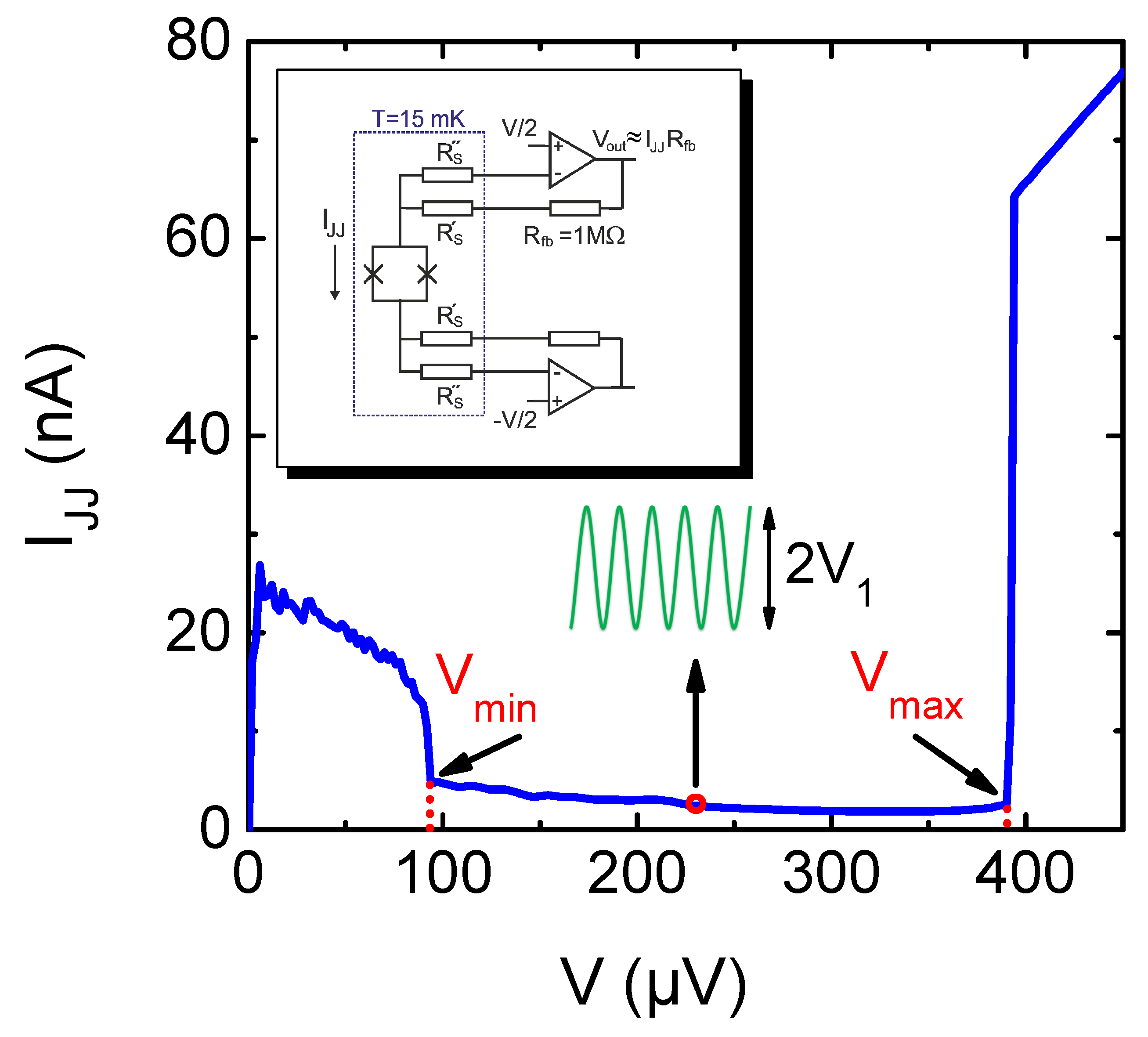
2.2. Josephson Junction Microwave Source

As a local microwave radiation source, we have employed the AC-Josephson effect, linking—by the Josephson relation—the oscillation frequency f J to the average voltage V JJ across the tunnel junction [27]. Generally, the Josephson oscillations involve an infinite set of harmonics of the fundamental frequency f J = V JJ / Φ 0 , where Φ 0 = h / 2 e is the flux quantum, but under certain conditions (see [24] for details), the oscillation amplitude of higher harmonics can be made negligibly small compared to the fundamental one, thus resulting in a quasi-monochromatic signal with the amplitude [28]
V 1 V C 1 + ( β C V JJ V C ) 2 ,
where β C 2 π Φ 0 I C R S 2 C J is the McCumber–Stewart damping parameter [29,30], V C I C R S is the junction characteristic voltage, C J the junction capacitance and R S the effective shunt resistance (made up, in our case, of serial bias resistances attached to the junction, cf., [15,16]).
Actually, our Josephson junction source consists of a small SQUID (comprising two nominally identical Al/AlO x /Al tunnel junctions, with total normal resistance R N 5 kΩ) which enables tuning the critical current and, therefore, the generated microwave power by applying a magnetic field. The critical current modulation period is Δ B = Φ 0 / A 5 m T , where A 0.4 µm 2 is the effective SQUID loop area. As the on-chip rf-shunting elements (see inset of Figure 3), we used serial thin film resistors made of double layer AuPd/TiO x ( 5 / 30 n m ) [24,31] with a square sheet resistance r 80 Ω / . The resistors were placed close to the device in order to minimize the capacitive contributions of the leads, C L 0 . 1 p F , to the small junctions’ capacitance, C J 5 f F C L , which otherwise would dramatically reduce the oscillation amplitude as a result of a large effective value of β C (see Equation (1)).
Figure 3. Measured I-V curve of the Josephson source at T 15 m K and B = 0. The operating points of this device, used for microwave signal generation, lie in the voltage range 100 µV V ( = V JJ ) 400 µV. Inset shows the equivalent biasing circuit for I-V curve measurement employing a transimpedance amplifier.
Applsci 06 00035 g003
Figure 3 depicts one of the measured I-V curves of the SQUID circuit at T 15 m K . The device is biased with a standard transimpedance amplifier as a feedback-controlled DC voltage source (see inset of Figure 3). Using the transimpedance amplifier and 4-point connection layout made it possible to circumvent the contribution of the cryostat wiring to the DC loading curve of the source and on this way to realize an almost perfect DC voltage bias for the SQUID. Continuous quasi-monochromatic microwave oscillation (with a stable Josephson voltage V JJ = V ) is expected in the subgap branch of the I-V curve, extending up to the voltages V V max = 2 Δ / e . For Al tunnel junctions, V max 400 µV ( f max = 4 Δ / h 200 G H z ) . At larger bias voltages, the strong DC quasiparticle current ( > 65 n A ) leads to the overheating of the junctions and generation of recombination phonons. On the other hand, at V < V min 100 µV, the value of V JJ is unstable due to the phase retrapping effect [32], and the junction state alternates between the supercurrent and the quasiparticle branch.
Using serial, instead of parallel, shunting resistors to the SQUID results in a low DC current through these resistors (equal in total to the current through the SQUID) and, consequently, low dissipated power. This, in turn, keeps the electron temperature in these resistors at a relatively low value, T e 70 mK, resulting in a negligible black-body radiation and also a low thermal noise contribution to the oscillations’ linewidth (2 Γ J T e ) in the subgap branch of the device I-V curve. Our estimations [24] also show a negligible shot noise contribution to the linewidth ( I qp ) almost one order of magnitude lower than that of thermal noise, due to a very low subgap quasiparticle current I qp < 5 n A visible in Figure 3. The effective shunt resistance R S is determined at microwave frequencies by a parallel combination of the transmission line (coupling element) wave impedance and two serial on-chip resistors R S (see Section 2.3). The measured and estimated parameters for one of the devices are presented in Table 2.
Table 2. Summary of measurement values of R N , R S , I C and f min , max V min , max / Φ 0 at T 15 m K and also estimations of SQUID parameters C J , β C , V C , V 1 , T e and Γ J . Values V 1 and T e are estimated at V JJ = 300 µV ( f J 145 G H z ).
Total Tunnel Area C J R N R S I C β C V C V 1 T e f min f max Γ J / 2 π
(µm 2 ) ( fF ) (kΩ) ( Ω ) ( nA ) (µV) ( µ V ) (mK)(GHz)(GHz)
0.154.9210320.026.74.86850–1900.9

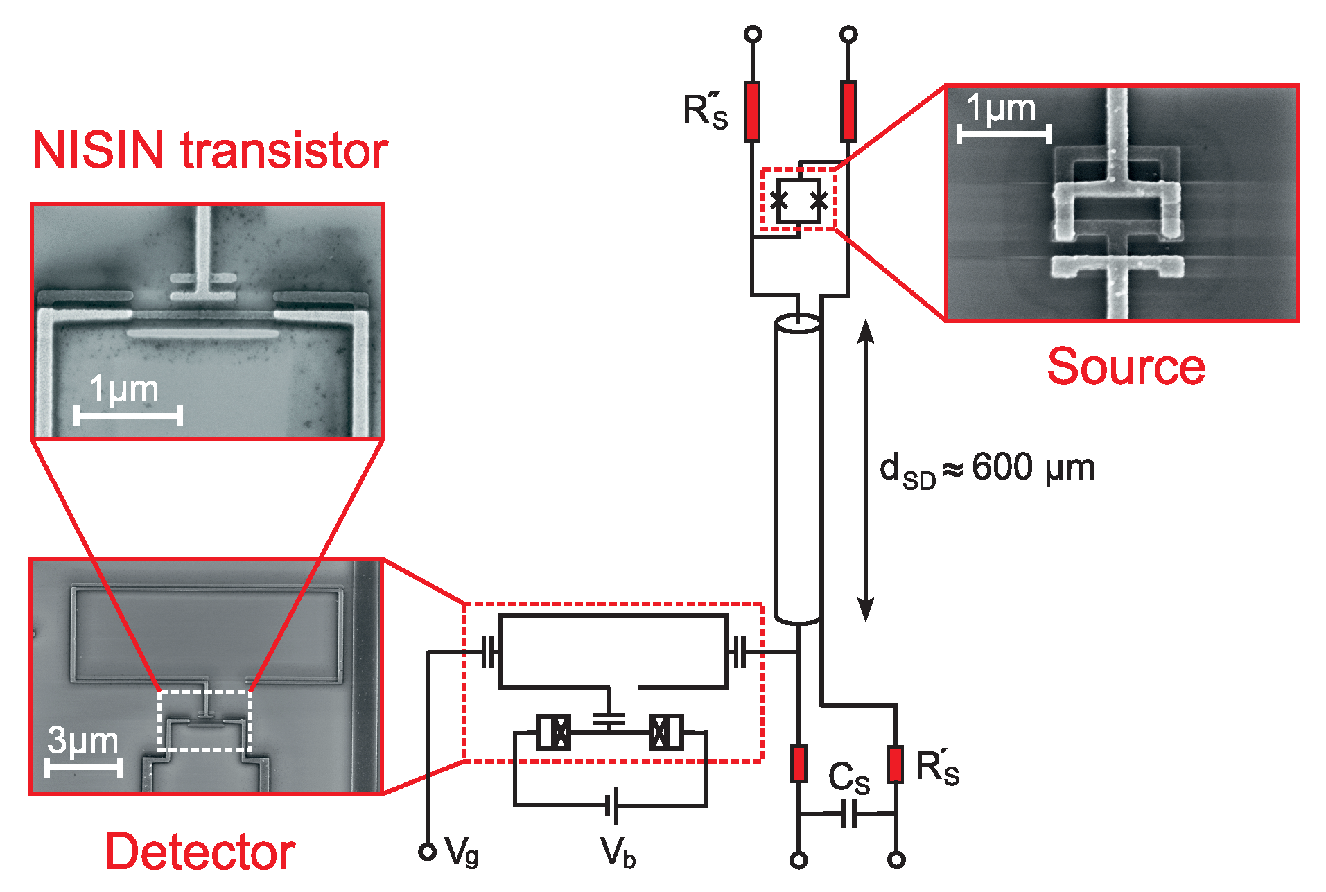
2.3. Coupling Method and Device Layout

To deliver the signal from the generator to the detector, a two-wire coplanar transmission stripline was designed and implemented bearing in mind that the source is put apart from the detector (cf., [19]) and, in this way, a possible contribution of phonon mediated signals is reduced. Figure 4 shows schematically the layout of the fabricated chips including the source, the detector and the coupling element. The line was designed to have a relatively high characteristic impedance Z 0 250 Ω as compared to a standard value of 50 Ω, which was carried out with the purpose of increasing the amplitude V 1 V C I C Z 0 . The line consists of two Al thin film microstrips, 50 µm apart, each with a width of 1 µm, thickness 80 n m and with a length d SD 600 µm which is comparable to the typical wavelength of the microwave signal emitted by the source ( λ 1 m m ). To avoid signal reflection, the line was terminated by a matched load consisting of two on-chip resistors R S 120 Ω and an interdigital capacitor C S 0 . 1 p F . Voltage is measured via two other leads, each equipped with an on-chip resistor R S = 4 R S 480 Ω.
Figure 4. Equivalent diagram of the complete circuit consisting of the source, the detector and the transmission line coupling. (Lower left inset): SEM picture of the detector circuit; (Upper left inset): Close-up SEM picture of the detector showing the NISIN transistor structure; (Upper right inset): SEM picture of the SQUID (microwave source).
Applsci 06 00035 g004
For comparison, we had also realized other ways of device coupling, first, in the form of a direct capacitive coupling using a 100 µm long Al thin film microstrip line connected to the Josephson source on one side and coupled capacitively to the floating gate on the other side. The length of this coupling line is intentionally chosen to be shorter in order to avoid possible resonances and reduce the losses. Furthermore, an extra source which was not coupled electromagnetically was placed on each chip at the same distance from the detector, to evaluate the possible contribution of substrate-mediated phonons to the detector signal.

3. Experimental Setup and Results

The fabricated chips were mounted into a microwave-tight (although not vacuum-tight) single-wall-shielded sample holder and measured in a dilution refrigerator with a base temperature T 15 m K . Each signal line was equipped with a Thermocoax coaxial filter [33] having a 1 m length and located at mK-stage of the fridge. The measurement results including the dependence of the detector signal on the frequency and power of microwave radiation as well as the contribution of the substrate-mediated phonons are presented in the following subsections.

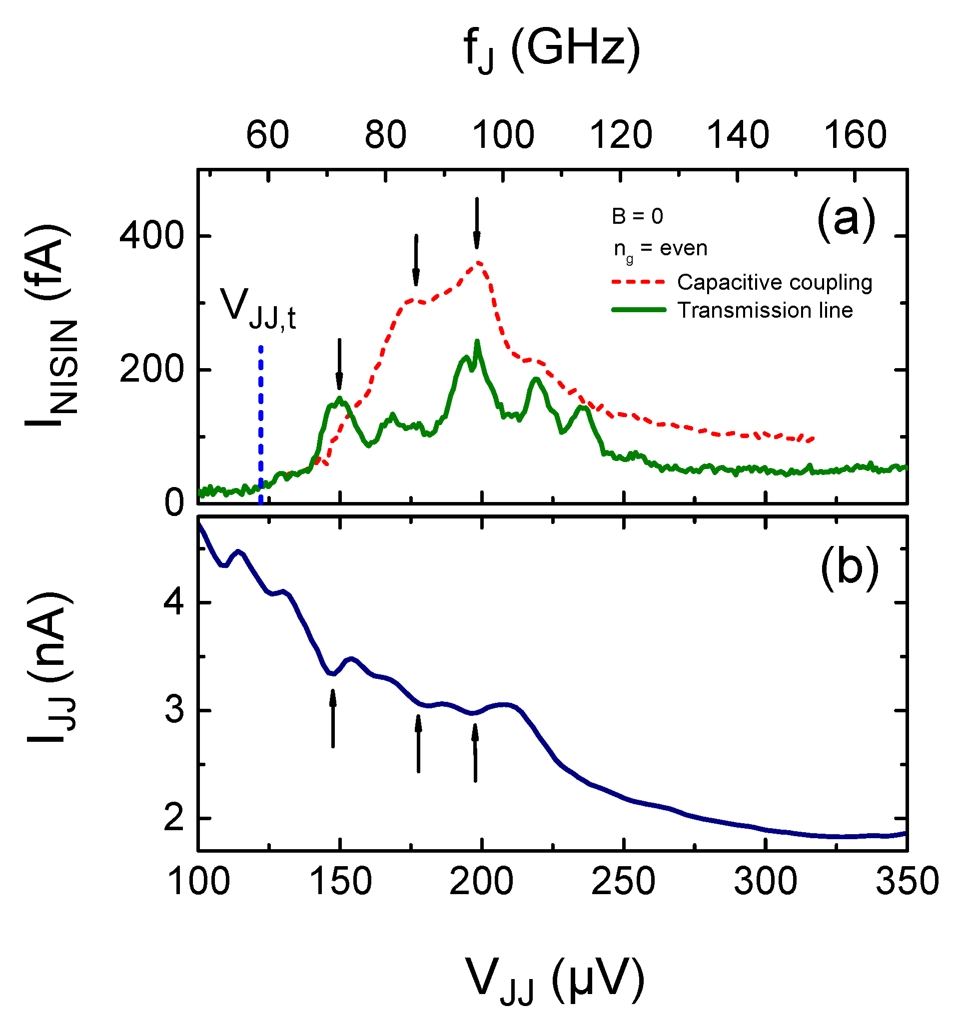
3.1. Frequency Dependence of the Response

We observed a dramatic change in the detector output caused by the microwave signal generated on-chip by the Josephson source. Figure 5 shows the detector current as a function of the detector bias and gate voltages when the source is turned off (panel (a)) and when the voltage across the source junctions is tuned to V JJ 200 µV ( f J 100 G H z ) corresponding to the maximum detector signal (panel (b)). Without irradiation, see Figure 5a, the current I NISIN is a 2e-periodic function of n g , which is in accordance with the model described in Section 2.1, since the tunneling is only possible for odd values of n g . At even values of n g the detector current is low and basically reduces to the dark signal appearing due to the background microwave radiation. As a result of the microwave irradiation coming from the source, a significant current appears also for the even settings of n g and, for the sufficiently strong microwave signal, approaches the value measured for odd n g (see right and upper panels in Figure 5b). We also note that the Andreev reflection does not contribute significantly to the transport mechanism since we do not observe the Andreev peaks in our measurements (in contrast to [25], where these peaks were clearly observed in subgap voltages and at odd values of n g ).
Figure 5. Detector current, I NISIN , measured as a function of the gate and bias voltages at zero magnetic field, (a) without irradiation and (b) under irradiation, when the source voltage is set to V JJ 200 µV > E t e v e n / 2 e generating microwave signal with frequency f J 100 G H z .
Applsci 06 00035 g005
The frequency dependence of the detector response is shown in Figure 6a (green curve) for the subgap Josephson source voltages. The response signal appears above the threshold voltage V JJ , t 120 µV ( f t = V JJ , t / Φ 0 58 G H z , marked by the blue dashed line in Figure 6a) corresponding to the activation energy E t e v e n 240 µeV calculated for the parameters of the experiment. After achieving a broad maximum in the voltage range 150 µV V JJ 250 µV, the detector current gradually decreases as, presumably, a result of reducing the radiation effect at higher photon energies 2 e V JJ (see Section 4).
The response was also featured by a set of resonances. This occurs even in spite of the fact that the transmission line is terminated to a matched load. In order to get an insight in the origin of the observed resonances, we compared the detector signal to that measured using a direct capacitive coupling (red dashed curve). As is seen in Figure 6a, the resonances are located approximately at the same frequencies for both types of the coupling, although for capacitive coupling these are rather smooth. We also found out that these locations did not substantially change when using a double thick Si substrate with the purpose of reducing the resonance frequency of the possible standing waves to the metallic sample table. We also noticed some peculiarities occurring almost at corresponding voltages in the autonomous I-V curve of the Josephson source as depicted in Figure 6b. As a possible explanation, we attribute these features to resonances in the on-chip wiring being identical in both layouts.
Figure 6. (a) The detector response as a function of the frequency of the microwave irradiation generated at V JJ < V max . The signal delivered over the transmission line (green curve) is compared to that over the capacitive coupling (red dashed curve). The stronger response in the sample with the capacitive coupling appears due to the larger value of critical current, I C 48 n A , than in that with the transmission line, I C 32 n A ; (b) An I-V curve measured in the same voltage range for one of the Josephson sources. Those peculiarities which coincide with observed peaks in the detector responses are marked by black arrows.
Applsci 06 00035 g006

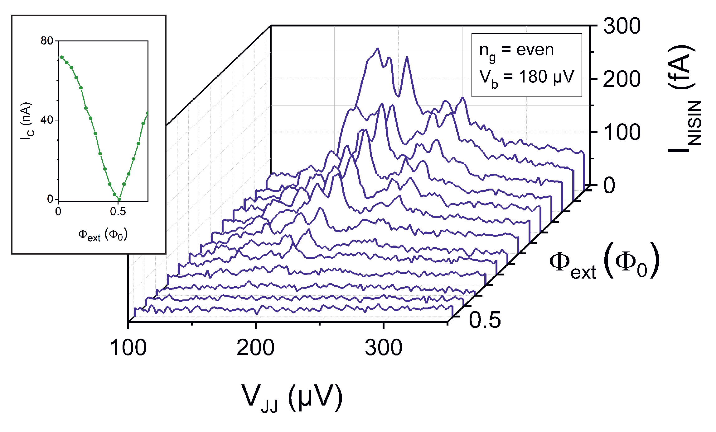
3.2. Periodic Modulation of the Source Power

The power tunability of the source was investigated using critical current modulation, I C ( Φ ext ) = I C ( 0 ) | cos ( π Φ ext / Φ 0 ) | , by applying the external magnetic field to the SQUID. The suppression of the Josephson supercurrent resulted in the reduction and, finally at Φ ext = Φ 0 / 2 , the vanishing of the detector response, as is shown in Figure 7, over the frequency range of interest and for a change in the magnetic flux from 0 up to Φ 0 / 2 ( B 0 ÷ 2 . 5 m T ). By further increasing the magnetic field up to a value B 20 m T , we observed a quasi-periodic modulation of the detector response (Figure 8) with a period Δ Φ ext Φ 0 . We consider this behavior to be a direct confirmation of the detector response being caused by the microwave signal generated by the Josephson source.
Figure 7. The detector response to the increase in the magnetic flux from 0 up to the value Φ 0 / 2 . The gradual decay of the response is a result of decreasing the source critical current (see inset) and, therefore, the radiation power to a vanishing value.
Applsci 06 00035 g007
Figure 8. Normalized detector response as a function of the magnetic flux (green curve). The red dotted curve is a phenomenological fit including an exponential decay expression shown in the figure.
Applsci 06 00035 g008
Figure 8 also shows a reduction in the height of the maximum detector current with increasing the applied magnetic flux. This behavior was observed even in spite of a true periodic modulation of the critical current. Taking into account a quadratic dependence of the emitted power on the resulting critical current and field-dependent losses in the transmission line, we were able to fit this decay by introducing phenomenologically an exponential prefactor and assuming the dependence as: I NISIN I C 2 ( Φ ext ) e 2 α Φ ext / Φ 0 . The result of fitting is depicted in Figure 8 with a red dotted curve using a value of 0 . 26 for the dimensionless coefficient α. The power losses in the transmission line are evaluated at B 20 m T being on the level of ∼ 0.01 dB/µm. We attribute the appearance of appreciable losses in the superconducting microstrip line to the formation of the mixed state in Al film related to the penetration of the magnetic field applied perpendicular to the film surface [34,35]. According to our estimations made for the present layout of the coplanar wave guide, the observed level of signal damping corresponds to an effective unit length flux flow resistance up to r 100 GHz 0.7 Ω/µm at B 20 m T . The obtained value is on the scale with DC unit length resistance r DC 0.5 Ω/µm, measured under the same conditions, and shares the same order with the normal state resistance of Al, r n (0.1–1) Ω/µm.

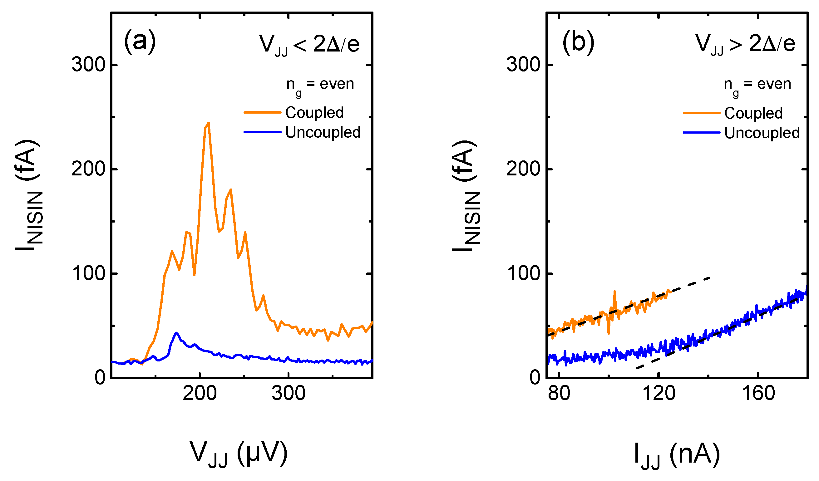
3.3. Effect of Emitted Phonons

To study possible effects of the substrate-mediated phonons on the detector output, an electromagnetically uncoupled reference source was used, positioned at the same distance from the detector as the coupled one. We measured the detector response for both sources operating in the subgap and above gap regimes. Figure 9a shows the detector response for an electromagnetically coupled (orange curve) source and an uncoupled (blue curve) source in subgap voltages, V JJ < 2 Δ / e . The detector response to the uncoupled source signal, scaled by the square of the critical current ratio, is substantially weaker (almost up to an order of magnitude) compared to the coupled source, and we found it to be gradually vanishing in the same manner as observed for the coupled source (see Figure 7), when sweeping the magnetic flux from 0 to Φ 0 / 2 (the curve not shown). On the contrary, the detector current responding to the quasiparticle current at V JJ > 2 Δ / e in either of the Josephson sources increases with a similar linear slope (see Figure 9b) indicating a comparable rise in the counting rate for the same increase of the quasiparticle generation (and recombination) rate both in the coupled and in the uncoupled sources. We attribute this behavior to the contribution of the recombination phonons [36,37] propagating via the substrate and achieving the detector after traveling over similar distances from both sources.
Figure 9. (a) The detector signal for the coupled (orange curve) and the uncoupled source (blue curve) operating in the subgap voltage region. The signal of the uncoupled source was scaled down by a factor ( I C , Coupled / I C , Uncoupled ) 2 = 0 . 28 for the sake of adequate comparison to account for the difference in the radiated microwave power. The coupled and uncoupled source critical currents are different due to technological reasons; (b) The detector signals for the same two sources biased in the quasiparticle branch V JJ > 2 Δ / e . The signal increases with the same slope for both sources (black dashed lines).
Applsci 06 00035 g009

4. Discussion

Two important characteristics of the NISIN detector will be addressed below in more detail with the help of a theoretical analysis of tunneling rates: the amplification factor and the device resolution in respect of the lowest absorption rate of the microwave photons.
In order to evaluate the amplification factor G, we calculated the photon-assisted quasiparticle tunneling rate Γ ph = Γ ph ( E ph ) , where E ph = 2 e V JJ = h f J is a photon energy corresponding to the Josephson frequency, and compared it with the value I NISIN / e measured in experiment. The NISIN transistor was assumed to be symmetrical, and the calculation was carried out for the gate setting n g 0 corresponding to the highest device sensitivity. At low experimental temperature, T 15 mK, and small energy k B T 1 µeV e V b 200 µeV, the main direction of tunneling is basically defined by the bias voltage V b and only two photon-assisted tunneling processes (one in each of the junctions, L and R, see Figure 1) dominate in creation of quasiparticles in the superconducting island, so that Γ ph Γ ph L + Γ ph R .
In order to calculate the tunneling rates Γ ph R , L , we follow the argument of [38] based on the P-function theory [39]. In particular, we assign the role of the noise source as in [38] to the Josephson oscillations in our case and make use of the low impedance of the current leads attached to the NISIN double junction. Thus, the function P ( E ) peaks around E = 0 and for substantially negative energy values, E < k B T , the value of P ( E ) is determined by its radiation-induced component [38]
P ( E ) = π S V ( | E | / ) R k E 2 ,
with R k = h / e 2 26 kΩ being the resistance quantum and S V ( ω ) the spectral density of the voltage oscillations appearing across the NIS junction under study due to the Josephson radiation. The physical meaning of the function P ( E ) is the probability for the tunneling electron to release energy E into or absorb it from the electromagnetic environment [39]. Furthermore, we take into account a narrow linewidth of Josephson oscillations in our source (see Table 2) and approximate the Lorentzian shape of the spectral function S V ( ω ) by the delta function, thus obtaining a simplified expression for P ( E )
P ( E ) π V A 2 4 R k × 1 E 2 × δ | E | E ph .
Here V A = a V 1 is an amplitude of voltage oscillations across the NIS junction generated by the Josephson source and delivered by the transmission line. The factor a = 2 C eff E C / e 2 = C eff / C Σ 0.028 is the coupling coefficient of the transmission line to the transistor island. The effective coupling capacitance C eff of the superconducting island to the transmission line was obtained from the DC modulation period of the NISIN transistor. For simplicity, we also neglect the losses in the transmission line (we consider the case B = 0 ), which should however look plausible once we have found the output signals measured for both types of the coupling methods, i.e., the transmission line and the capacitive coupling, to be comparable.
Taking advantage of the low temperature T 15 mK, we can make use of the zero-temperature approximation and replace the Fermi factors by corresponding step functions, thus obtaining a simplified standard golden rule formula [40]
Γ ph ( E ) 1 e 2 R T E d E n Δ d E s n s ( E s ) P ( E n E s ) ,
where n s ( E ) = E / E 2 Δ 2 is a BCS density of states in the superconducting island. The integral can be taken analytically resulting in
Γ ph L , R ( E ph ) | E ph = 2 e V JJ Δ 8 R T V A ( V JJ ) E ph 2 E ph E t L , R Δ + 1 2 1 ,
where E t L , R is the activation threshold for tunneling of an electron in a left (right) junction of the NISIN transistor, respectively.
In Figure 10, we plotted a set of Γ ph vs. V JJ dependencies calculated for an NISIN detector tuned to slightly different gate voltages around n g = 0 . The curves exhibit discontinuities in the derivative at the tunneling threshold in the individual junctions, which would, however, be smeared in a more realistic approximation considering a finite linewidth of Josephson oscillations, a finite impedance of the environment or non-zero T. As expected, the activation threshold achieves its highest value in the point, n g = 0 , of the maximum Coulomb blockade. The decay at higher voltages is partially related to the decay of the Josephson oscillation amplitude V 1 ( V JJ ) , see Equation (1).
Figure 10. The rate Γ ph of photon-assisted generation of quasiparticles in the superconducting island calculated as a function of mean voltage across the Josephson source, for three slightly different gate settings around the even state n g = 0 . For the parameters of the circuit used in the calculation, see Table 1 and Table 2.
Applsci 06 00035 g010
Two important conclusions can be derived from the calculated curves. First, for the Josephson voltages noticeably exceeding the activation thresholds V JJ , t , the rate Γ ph becomes independent of the gate voltage. As a result, the response should be insensitive to a small variation of the offset (background) charges. Second, the comparison of the experimental response current I NISIN 200 fA (see Figure 6a, the data for transmission line) with the calculated rate Γ ph (200 µV) ≈ 700 Hz (see Figure 10) gives rise to the amplification factor G 200 fA / ( e × 700 Hz) 1 . 8 × 10 3 . The lowest measurable photon-assisted tunneling rate is then as low as about δ Γ ph δ I NISIN / e G 35 photons per second, corresponding to the noise-limited current resolution δ I NISIN 10 fA achieved in our experiment by averaging the transistor output signal over the time of 1 s. Even a higher resolution can be expected in the case of using lower noise electronics for femtoampere current measurement. A relatively high value of G 10 3 obtained in our study noticeably exceeds G 40 reported in [20]. We attribute this difference presumably to a high quality of superconducting Al film evaporated in our dedicated ultrahigh vacuum system which ensures a low density of impurity domains in the island resulting in a low rate of quasiparticle relaxation.

5. Conclusions

To conclude, we fabricated and studied at 15 mK a microwave circuit combining on the same chip a Josephson junction microwave source and an SET-based photon detector with a superconducting island as a sensitive element. The results obtained at the frequencies around ∼100 GHz demonstrate a high microwave photon sensitivity of the detector, which we estimate to be on the level of a few tens of photons absorbed per second. The magnitude of the response was confirmed to be tunable by choosing the operating point of the Josephson microwave source. We found the contribution of phonons propagating over the substrate to be negligible in the frequency range below about 150 GHz, but increasing monotonously with the quasiparticle current in the Josephson junction source in the above-gap regime. Further study and improvement of the electronics setup would be helpful to verify and to improve the counting resolution of the detector down to a level of single photons.

Acknowledgments

Technological assistance from Thomas Weimann and Viktor Rogalya is appreciated. Fruitful discussions with Jukka P. Pekola and Ville F. Maisi are acknowledged. This work was funded by the Joint Research Project MICROPHOTON. Joint Research Project MICROPHOTON belongs to the European Metrology Research Programme (EMRP). The EMRP is jointly funded by the EMRP participating countries within EURAMET and the European Union.

Author Contributions

Behdad Jalali-Jafari performed the device fabrication, analyzed the results and prepared the manuscript. Sergey V. Lotkhov set up the complete experiment, carried out the low temperature measurements and theoretical calculations, and also revised the manuscript. Alexander B. Zorin provided conceptual support and revised the manuscript.

Conflicts of Interest

The authors declare no conflict of interest.

References

  1. Pothier, H.; Lafarge, P.; Orfila, P.F.; Urbina, C.; Esteve, D.; Devoret, M.H. Single electron pump fabricated with ultrasmall normal tunnel junctions. Phys. B 1991, 169, 573–574. [Google Scholar] [CrossRef]
  2. Pekola, J.P.; Vartiainen, J.J.; Möttönen, M.; Saira, O.-P.; Meschke, M.; Averin, D.V. Hybrid single-electron transistor as a source of quantized electric current. Nat. Phys. 2008, 4, 120–124. [Google Scholar] [CrossRef]
  3. Averin, D.V.; Pekola, J.P. Nonadiabatic charge pumping in a hybrid single electron transistor. Phys. Rev. Lett. 2008, 101. [Google Scholar] [CrossRef] [PubMed]
  4. Keller, M.W.; Eichenberger, A.L.; Martinis, J.M.; Zimmerman, N.M. A capacitance standard based on counting electrons. Science 1999, 285, 1706–1709. [Google Scholar] [CrossRef] [PubMed]
  5. Camarota, B.; Scherer, H.; Keller, M.W.; Lotkhov, S.V.; Willenberg, G.-D.; Ahlers, F.J. Electron counting capacitance standard with an improved five-junction R-pump. Metrologia 2012, 49, 8–14. [Google Scholar] [CrossRef]
  6. Pekola, J.P.; Saira, O.-P.; Maisi, V.F.; Kemppinen, A.; Möttönen, M.; Pashkin, Y.A.; Averin, D.V. Single-electron current sources: Toward a refined definition of the ampere. Rev. Mod. Phys. 2013, 85, 1421–1472. [Google Scholar] [CrossRef]
  7. Wendin, G.; Shumeiko, V.S. Superconducting Quantum Circuits, Qubits and Computing. In Handbook of Theoretical and Computational Nanotechnology; Rieth, M., Schommers, W., Eds.; American Scientific Publishers: Los Angeles, CA, USA, 2006; Volume 3, pp. 223–309. [Google Scholar]
  8. Devoret, M.H.; Martinis, J.M. Implementing qubits with superconducting integrated circuits. Quantum Inf. Process. 2004, 3, 163–203. [Google Scholar] [CrossRef]
  9. Kautz, R.L.; Keller, M.W.; Martinis, J.M. Noise-induced leakage and counting errors in the electron pump. Phys. Rev. B 2000, 62, 15888–15902. [Google Scholar] [CrossRef]
  10. Pekola, J.P.; Maisi, V.F.; Kafanov, S.; Chekurov, N.; Kemppinen, A.; Pashkin, Y.A.; Saira, O.-P.; Möttönen, M.; Tsai, J.S. Environment-assisted tunneling as an origin of the Dynes density of states. Phys. Rev. Lett. 2010, 105. [Google Scholar] [CrossRef] [PubMed]
  11. Di Marco, A.; Maisi, V.F.; Hekking, W.J.; Pekola, J.P. Effect of photon-assisted Andreev reflection in the accuracy of a SINIS turnstile. Phys. Rev. B 2015, 92. [Google Scholar] [CrossRef]
  12. Kemppinen, A.; Lotkhov, S.V.; Saira, O.-P.; Zorin, A.B.; Pekola, J.P.; Manninen, A.J. Long hold times in a two-junction electron trap. Appl. Phys. Lett. 2011, 99. [Google Scholar] [CrossRef]
  13. Barends, R.; Wenner, J.; Lenander, M.; Chen, Y.; Bialczak, R.C.; Kelly, J.; Lucero, E.; O’Malley, P.; Mariantoni, M.; Sank, D.; et al. Minimizing quasiparticle generation from stray infrared light in superconducting quantum circuits. Appl. Phys. Lett. 2011, 99. [Google Scholar] [CrossRef]
  14. Astafiev, O.; Komiyama, S.; Kutsuwa, T.; Antonov, V.; Kawaguchi, Y.; Hirakawa, K. Single-photon detector in the microwave range. Appl. Phys. Lett. 2002, 80, 4250–4252. [Google Scholar] [CrossRef]
  15. Deblock, R.; Onac, E.; Gurevich, L.; Kouwenhoven, L.P. Detection of quantum noise from an electrically driven two-level system. Science 2003, 301, 203–206. [Google Scholar] [CrossRef] [PubMed]
  16. Billangeon, P.-M.; Pierre, F.; Bouchiat, H.; Deblock, R. Very high frequency spectroscopy and tuning of a single-Cooper-pair transistor with an on-chip generator. Phys. Rev. Lett. 2007, 98. [Google Scholar] [CrossRef] [PubMed]
  17. Chen, Y.-F.; Hover, D.; Sendelbach, S.; Maurer, L.; Merkel, S.T.; Pritchett, E.J.; Wilhelm, F.K.; McDermott, R. Microwave photon counter based on Josephson junctions. Phys. Rev. Lett. 2011, 107. [Google Scholar] [CrossRef] [PubMed]
  18. Lotkhov, S.V.; Saira, O.-P.; Pekola, J.P.; Zorin, A.B. Single-charge escape processes through a hybrid turnstile in a dissipative environment. New J. Phys. 2011, 13. [Google Scholar] [CrossRef]
  19. Lotkhov, S.V.; Zorin, A.B. A hybrid superconductor-normal metal electron trap as a photon detector. Appl. Phys. Lett. 2012, 100. [Google Scholar] [CrossRef]
  20. Maisi, V.F.; Lotkhov, S.V.; Kemppinen, A.; Heimes, A.; Muhonen, J.T.; Pekola, J.P. Excitation of single quasiparticles in a small superconducting Al island connected to normal-metal leads by tunnel junctions. Phys. Rev. Lett. 2013, 111. [Google Scholar] [CrossRef] [PubMed]
  21. Dolan, G.J. Offset masks for lift-off photoprocessing. Appl. Phys. Lett. 1977, 31, 337–339. [Google Scholar] [CrossRef]
  22. Niemeyer, J. Eine einfache Methode zur Herstellung kleinster Josephson-Elemente. PTB-Mitteilungen 1974, 84, 251–253. [Google Scholar]
  23. Lotkhov, S.V.; Camarota, B.; Scherer, H.; Weimann, T.; Hinze, P.; Zorin, A.B. Shunt-protected single-electron tunneling circuits fabricated on a quartz wafer. In Proceedings of the IEEE Nanotechnology Materials and Devices Conference, Traverse City, MI, USA, 2–5 June 2009.
  24. Jalali-Jafari, B.; Lotkhov, S.V.; Zorin, A.B. Al/AlOx/Al-Josephson-junction-based microwave generators for weak-signal applications below 100 mK. Available online: http://arxiv.org/abs/1410.5314 (accessed on 25 January 2016).
  25. Hergenrother, J.M.; Tuominen, M.T.; Lu, J.G.; Ralph, D.C.; Tinkham, M. Charge transport and photon-assisted tunneling in the NSN single-electron transistor. Phys. B 1994, 203, 327–339. [Google Scholar] [CrossRef]
  26. Eiles, T.M.; Martinis, J.M.; Devoret, M.H. Even-odd asymmetry of a superconductor revealed by the Coulomb blockade of Andreev reflection. Phys. Rev. Lett. 1993, 70, 1862–1865. [Google Scholar] [CrossRef] [PubMed]
  27. Josephson, B.D. Possible new effects in superconductive tunnelling. Phys. Lett. 1962, 1, 251–253. [Google Scholar] [CrossRef]
  28. Likharev, K.K.; Ulrich, B.T. Sistemi s Josephsonovskimi Kontaktami; Izdatelstro Moskovskogo Universiteta: Moscow, Russia, 1978; p. 58. (In Russian) [Google Scholar]
  29. McCumber, D.E. Effect of ac impedance on dc voltage-current characteristics of superconductor weak-link junctions. J. Appl. Phys. 1968, 39, 3113–3118. [Google Scholar] [CrossRef]
  30. Stewart, W.C. Current-voltage characteristics of Josephson junctions. Appl. Phys. Lett. 1968, 12, 277–280. [Google Scholar] [CrossRef]
  31. Lotkhov, S.V. Ultra-high-ohmic microstripline resistors for Coulomb blockade devices. Nanotechnology 2013, 24. [Google Scholar] [CrossRef] [PubMed]
  32. Likharev, K.K. Dynamics of Josephson Junctions and Circuits; Gordon and Breach science: New York, NY, USA, 1986. [Google Scholar]
  33. Zorin, A.B. The thermocoax cable as the microwave frequency filter for single electron circuits. Rev. Sci. Instrum. 1995, 66, 4296–4300. [Google Scholar] [CrossRef]
  34. Tinkham, M. Introduction to Superconductivity, 2nd ed.; Dover publications, Inc.: Mineola, NY, USA, 1996. [Google Scholar]
  35. Stan, G.; Field, S.B.; Martinis, J.M. Critical field for complete vortex expulsion from narrow superconducting strips. Phys. Rev. Lett. 2004, 92. [Google Scholar] [CrossRef] [PubMed]
  36. Schinner, G.J.; Tranitz, H.P.; Wegscheider, W.; Kotthaus, J.P.; Ludwig, S. Phonon-mediated nonequilibrium interaction between nanoscale devices. Phys. Rev. Lett. 2009, 102. [Google Scholar] [CrossRef] [PubMed]
  37. Gasser, U.; Gustavsson, S.; Küng, B.; Ensslin, K.; Ihn, T. Phonon-mediated back-action of a charge readout on a double quantum dot. Nanotechnology 2010, 21. [Google Scholar] [CrossRef] [PubMed]
  38. Martinis, J.M.; Nahum, M. Effect of environmental noise on the accuracy of Coulomb-blockade devices. Phys. Rev. B 1993, 48, 18316–18319. [Google Scholar] [CrossRef]
  39. Ingold, G.-L.; Nazarov, Y.V. Charge tunneling rates in ultrasmall junctions. In Single Charge Tunneling, Coulomb Blockade Phenomena in Nanostructures; Grabert, H., Devoret, M.H., Eds.; Plenum: New York, NY, USA, 1992; Volume 294, pp. 21–107. [Google Scholar]
  40. Merzbacher, E. Quantum Mechanics, 3rd ed.; John Wiley & Sons, Inc.: New York, NY, USA, 1998. [Google Scholar]

