Article

Simulation and Fabrication of HfO2 Thin Films Passivating Si from a Numerical Computer and Remote Plasma ALD

1
School of Opto-electronic and Communication Engineering, Fujian Provincial Key Laboratory of Optoelectronic Technology and Devices, Xiamen University of Technology, Xiamen 361024, China
2
Department of Materials Science and Engineering, Da-Yeh University, ChungHua 51591, Taiwan
3
Department of Physics, OSED, Xiamen University, Xiamen 361005, China
*
Author to whom correspondence should be addressed.
Appl. Sci. 2017, 7(12), 1244; https://doi.org/10.3390/app7121244
Submission received: 31 October 2017 / Revised: 24 November 2017 / Accepted: 27 November 2017 / Published: 1 December 2017
(This article belongs to the Special Issue Selected Papers from IEEE ICICE 2017)

Abstract

:
Recombination of charge carriers at silicon surfaces is one of the biggest loss mechanisms in crystalline silicon (c-Si) solar cells. Hafnium oxide (HfO2) has attracted much attention as a passivation layer for n-type c-Si because of its positive fixed charges and thermal stability. In this study, HfO2 films are deposited on n-type c-Si using remote plasma atomic layer deposition (RP-ALD). Post-annealing is performed using a rapid thermal processing system at different temperatures in nitrogen ambient for 10 min. The effects of post-annealing temperature on the passivation properties of the HfO2 films on c-Si are investigated. Personal computer one dimension numerical simulation for the passivated emitter and rear contact (PERC) solar cells with the HfO2 passivation layer is also presented. By means of modeling and numerical computer simulation, the influence of different front surface recombination velocity (SRV) and rear SRV on n-type silicon solar cell performance was investigated. Simulation results show that the n-type PERC solar cell with HfO2 single layer can have a conversion efficiency of 22.1%. The PERC using silicon nitride/HfO2 stacked passivation layer can further increase efficiency to 23.02% with an open-circuit voltage of 689 mV.

1. Introduction

Reduction of surface recombination is very important for crystalline silicon (c-Si)-based electronic devices, and especially for high-efficiency c-Si solar cells. Because of the increasing need for lower-cost silicon solar cells, as Si material has a rather high cost, thinner Si substrates are required. Conventional surface passivation for Si involves the formation of a thin silicon dioxide (SiO2) layer. However, this process requires a long period at high temperatures, leading to an increased thermal budget. Due to these process-related issues, low-temperature surface passivation methods for both heavily doped and moderately doped c-Si surfaces have been widely studied. Several materials such as SiC, a-Si:H, and Si3N4 have been considered for surface passivation [1]. Recently, Al2O3 films grown via atomic layer deposition (ALD) have been reported to have good surface passivation on p-type c-Si [2,3]. ALD provides a very precise control over the properties of the material, especially the uniformity and thickness of dielectric layers. However, an Al2O3 passivation layer has negative fixed charges, which result in an inversion layer on the n-type wafer surface, causing short-circuit current loss due to the parasitic shunting between this inversion layer and metal contact [4]. HfO2 films have positive fixed charges and this makes it very suitable for passivation of n-type silicon wafers. There is currently limited research focusing on the passivation of HfO2 on n-type silicon wafers for silicon solar cells [5,6].
In this work, the surface passivation properties of the HfO2 films deposited by a remote plasma atomic layer deposition system (RP-ALD) on n-type c-Si with different post-annealing temperatures are investigated. The structural changes and the electrical properties of the thin films induced by annealing temperature are characterized. Finally, PC1D (Version 5.9, University of New South Wales, Sydney, NSW, Australia, 2003) simulation for HfO2-passivated n-type silicon solar cells is presented.

2. Experimental

Double-sided polished (100)-oriented n-type 0.5–1 ohm-cm six-inch 200 µm thick Czochralski Si wafers were cleaned by a standard Radio Corporation of America method, and a 2% hydrogen fluoride-dip for 60 s was performed to remove stray oxides. Approximately 15 nm of HfO2 (168 cycles) were deposited by remote plasma ALD (Picosun R-200) (Picosun, Espoo, Finland) on the wafers using tetrakis(ethylmethylamino)hafnium (TEMAH) and oxygen as the precursors. The pulse times for TEMAH and O2 were 1.6 and 10 s, respectively. The nitrogen purge time was 10 s for both precursors. The plasma power was 2500 W. The substrate temperature was 250 °C. The post-deposition rapid thermal anneal was performed in N2 for 10 min, and the annealing temperature was varied from 400 to 650 °C to investigate the effect on surface passivation. The hydrogenated silicon nitride (SiNx:H)/HfO2 stacked layer was prepared and annealed at 500 °C. The SiNx:H layer with a thickness of 120 nm was deposited using radio-frequency inductively coupled plasma chemical vapor deposition with a gas mixture of trimethylsilane (TMS) and ammonia (NH3) at a temperature of 120 °C, a power of 1200 W, and a pressure of 5 mTorr. The flow rates of the TMS and NH3 were 35 and 25 sccm, respectively. The injection level-dependent minority carrier lifetime of the wafers was measured using quasi-steady-state photoconductance (Sinton Instruments WCT-120) (Sinton Instruments, Sinton, CO, USA). Assuming an infinite bulk lifetime, a maximum surface recombination rate Smax was calculated from the lifetime measurements as given by
S m a x = W 2 τ e f f
where W is the wafer thickness and τeff is the measured effective lifetime at an injection level of 1 × 1015 cm−3. For the capacitance–voltage (C–V) measurement, the MOS capacitors with an area of 2 × 10⁻³ cm2 were defined by evaporating of Au electrodes onto HfO2 in high vacuum (1 × 10⁻⁶ Torr). The positive oxide charge density (Qf) was extracted from the C-V curves as given by
Q f = ( φ m s V F B ) C o x q A
where ϕms is the work function difference between the metal and semiconductor, VFB is the flat band voltage, Cox is the oxide capacitance, q is the electron charge, and A is the electrode area. The interface charge density (Dit) was calculated from the conductance–voltage curves using the expression [7]
D i t = 2 ω C o x 2 G m a x q A ( G m a x 2 + ω 2 ( C o x C m G m a x ) 2 )
where Gmax is the maximum conductance, and Cm is the measured capacitance at a frequency ω. The bonding configuration of the HfO2 films was investigated by Fourier transformation infrared (FTIR) spectroscopy. The cross-sectional images of the HfO2 films were observed by transmission electron microscopy (TEM). The simulation of solar cell performance was carried out using PC1D computer software.

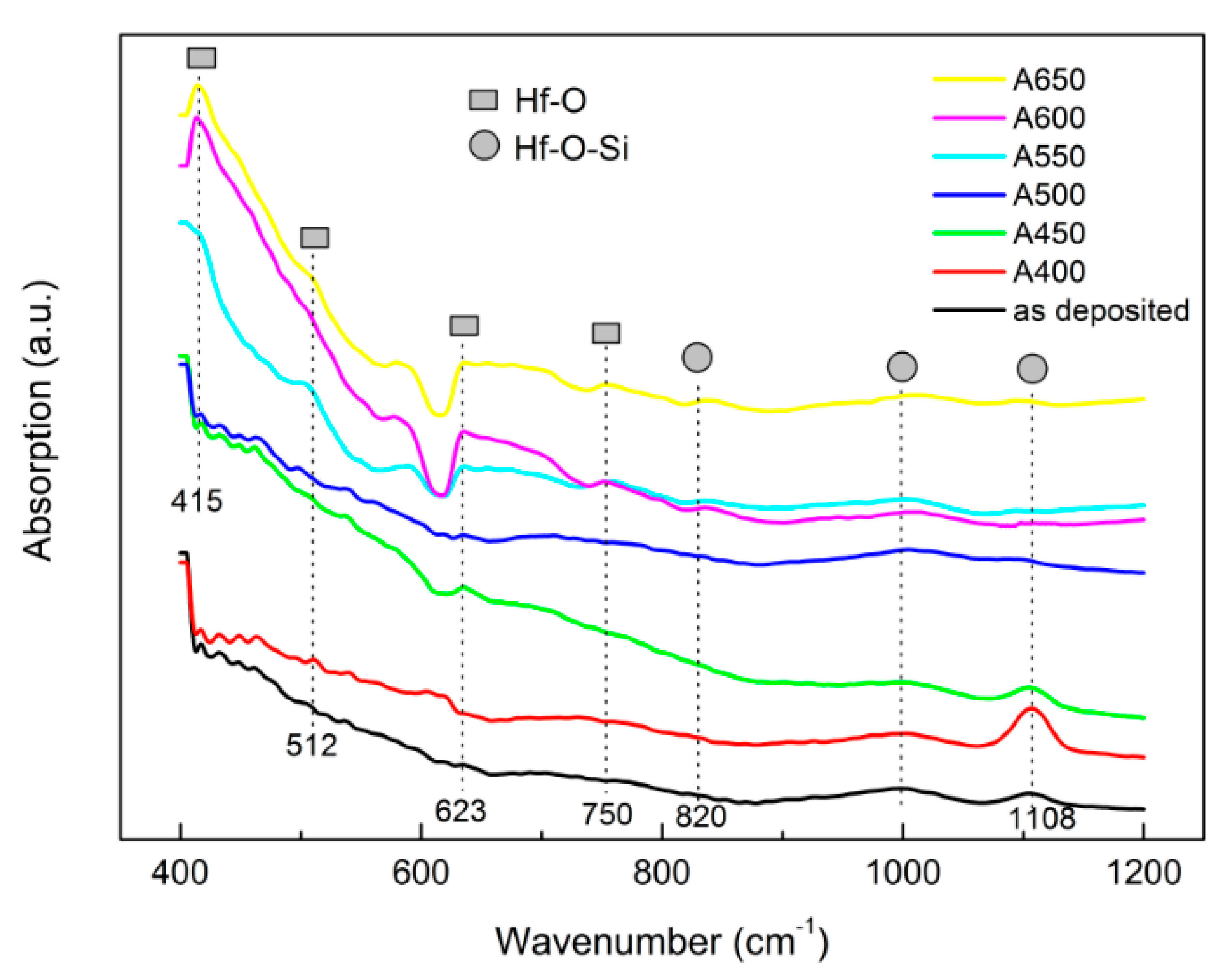
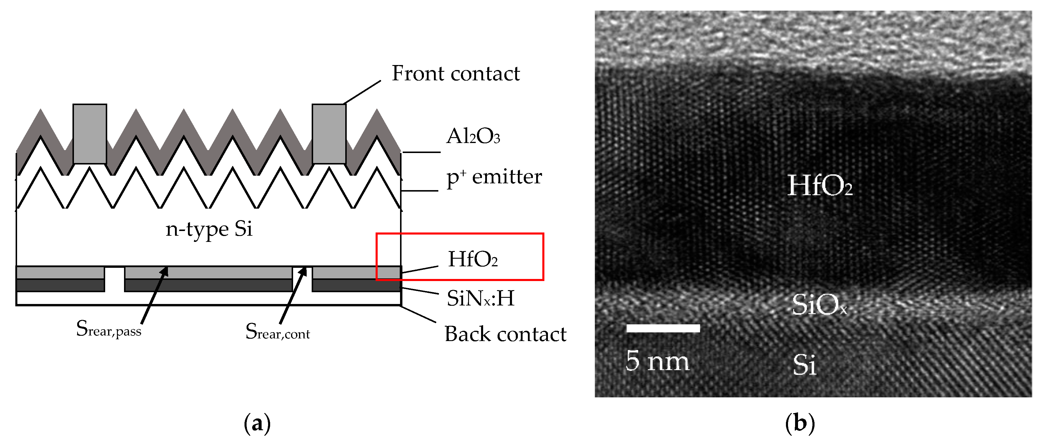
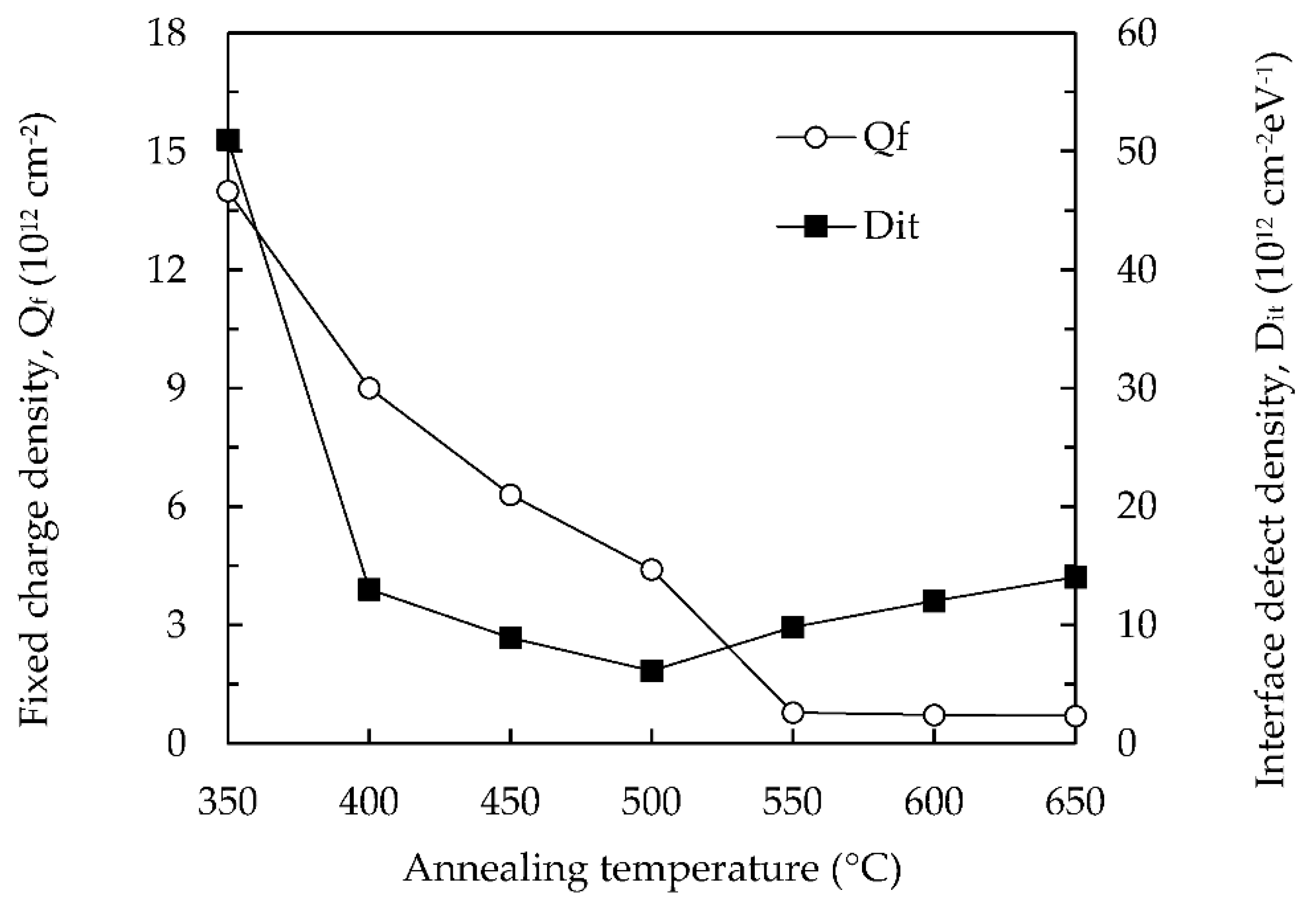
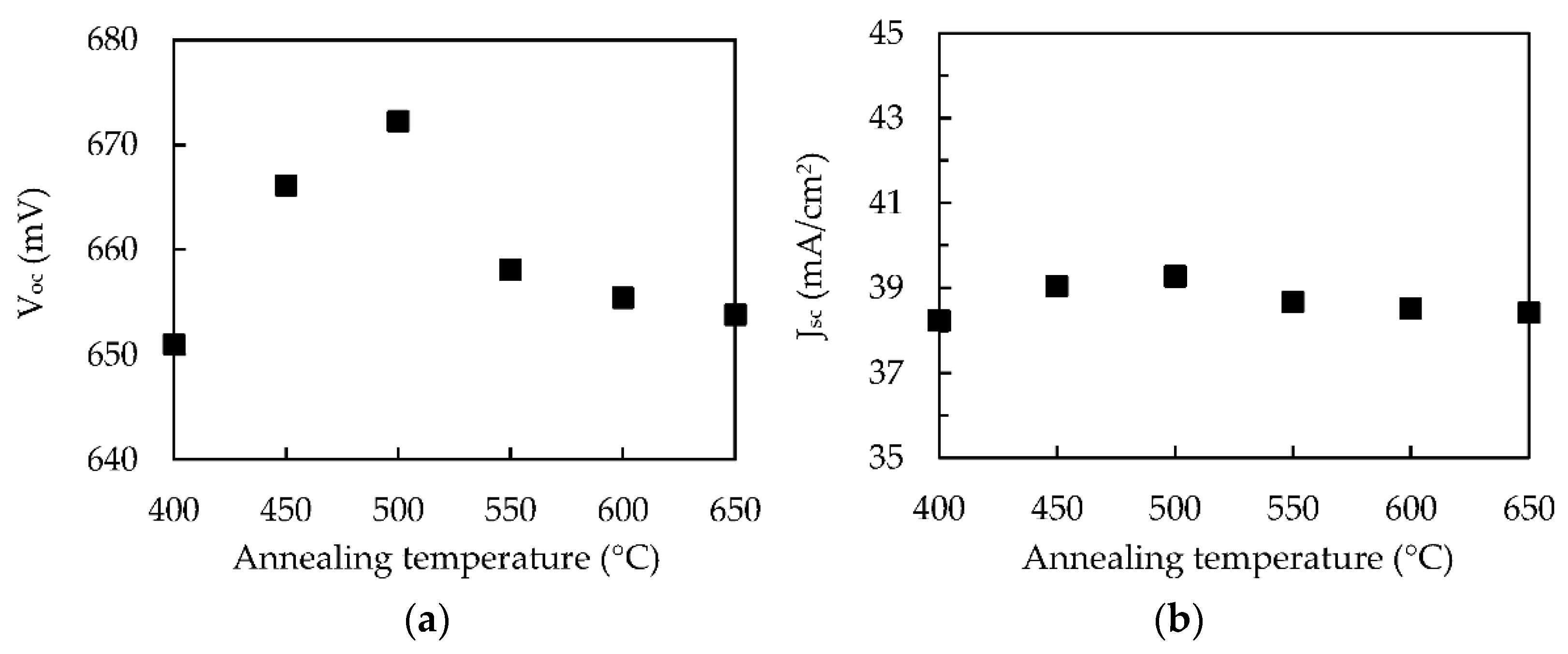
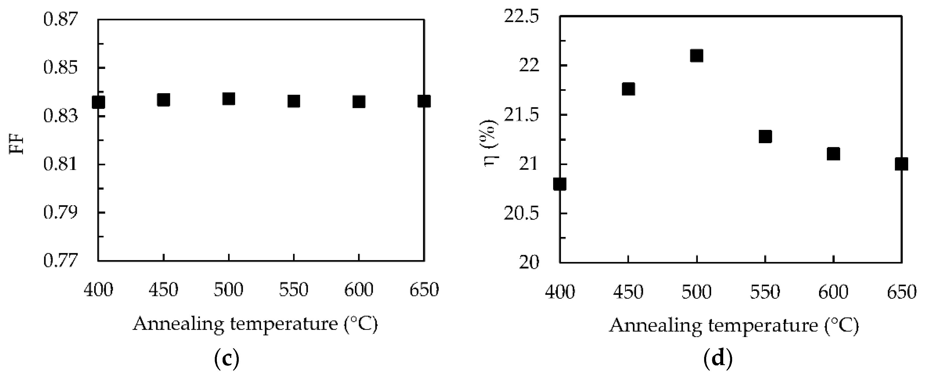
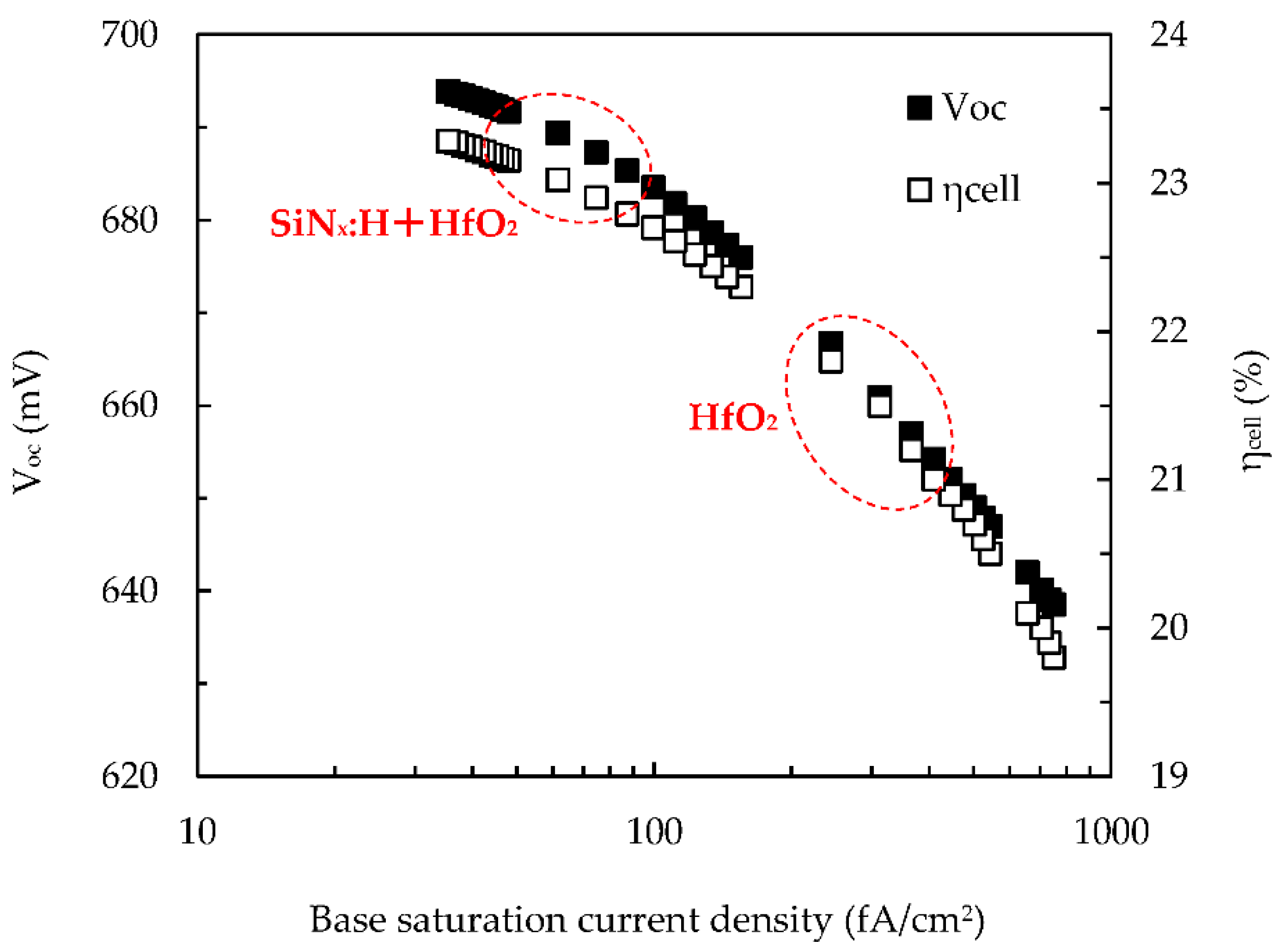
3. Results and Discussion

Figure 1 shows the FTIR spectra for the HfO2 films with different post-annealing temperatures ranging from 400 to 650 °C. The absorbance peaks at 415, 512, 600, 623, and 750 cm−1 are assigned to Hf–O bonding configuration [8,9,10,11]. The peaks at 820, 1000, and 1108 cm−1 correspond to the Si–O bonds in the films [8,9,10]. Considering the as-deposited HfO2 sample, the Si–O peak at 1108 cm−1 suggests that the as-deposited film already consists of an SiOx-like interfacial layer between the silicon wafer and HfO2 layer. This is similar to the Al2O3/Si system, which attributes the presence of the interfacial SiOx layer to the first few ALD cycles [12]. The SiOx peak intensity enhances at the annealing temperature of 400 °C, but it then drops when the annealing temperature further increases. For the annealing temperatures of 550–650 °C, the peak is almost unobservable, which in turn infers that these samples have nearly no SiOx interfacial layer. On the other hand, the intensity of the Hf–O peak at 623 cm−1 increases when the annealing temperature increases. The enhancement of the signal intensity may be a result of densification of the HfO2 films during the annealing process. It seems that there is a competitive process between the formation of Si–O and Hf–O bonds. Oxygen atoms bond to silicon atoms at low temperatures, but they are consumed by bonding to Hf under high-temperature annealing conditions. Varying the annealing temperature can therefore control the interfacial layer.
Figure 2a shows n-type PERC solar cell structure consisting of an Al2O3 emitter passivation layer and an HfO2 rear passivation layer. The TEM cross-sectional image of the HfO2/n-type Si interface annealed at 550 °C is shown in Figure 2b. The extent of the atom arrangement order can be used for evaluation of crystallization of films. It can be seen that the atoms in the HfO2 region are orderly arranged, indicating the high crystallinity achieved at the annealing temperature of 550 °C. The interfacial SiOx layer with a thickness of approximately 2.5 nm can be seen, but both sides of this interfacial layer are partially crystallized. It has been reported that HfO2 would be possibly crystallized at temperatures greater than 400 °C [13]. It should be noted that the interfacial layer in the as-deposited sample is approximately 3 nm of amorphous SiOx .The crystallization near the HfO2/SiO2 interface causes a thickness reduction in the actual amorphous SiOx layer. This phenomenon is more pronounced when the annealing temperature is elevated. In Figure 2b, the amorphous SiOx layer is significantly inhomogeneous, and the SiOx layer can hardly be distinguished in some regions. This is in agreement with the decreased signal intensity of SiOx found via FTIR, as it almost disappears at annealing temperatures greater than 550 °C. As the SiOx interfacial layer is usually considered to play an important role in decreasing the interface defect density in the dielectric/Si system [12], annealing temperatures equal to or higher than 550 °C are not preferable.
Figure 3 shows the Qf and Dit values obtained from C-V measurements as a function of annealing temperature. The as-deposited film has a high Qf value of 1.4 × 1013 cm−3. This might be due to the formation of the Si–O interfacial layer, which causes the Hf atoms near the interface region to bond with oxygen atoms in oxygen-poor conditions. The oxygen vacancies are known to be the main cause of positive charges in HfO2 films [14,15]. The Qf decreases from 9 × 10¹² to 6.9 × 1011 cm−2 when the annealing temperature increases from 400 to 650 °C. As shown by the FTIR results, the bonding configuration changes from Si–O to Hf–O, so the oxygen vacancies of HfO2 near the interface reduce when the annealing temperature increases. Another reason for the smaller Qf values of the annealed samples compared to the as-deposited one is the crystallization of HfO2 at these annealing temperatures. In particular, the HfO2 films are completely crystallized when the annealing temperature reaches 550 °C or above, leading to very low Qf values of around 0.5 × 1011 cm−2. The value of Dit decreases from 5.1 × 1013 cm−2eV−1 for the as-deposited sample to a minimum 6.1 × 1012 cm−2eV−1 for the sample annealed at 500 °C, and then increases to 1.4 × 1013 cm−2eV−1 when the temperature further increases to 650 °C. Several studies have suggested that interfacial SiOx plays a critical role in the reduction of interface defect density [12]. The high Dit of the as-deposited sample is due to the fact that SiOx deposited at low temperatures has many pores and defects near the SiOx/Si interface. Increasing the deposition temperature of SiOx can increase film density, therefore decreasing the Dit. However, for the annealing temperatures from 550 and 650 °C, the nearly disappeared SiOx interfacial layer is responsible for the increased Dit.
Table 1 lists the values of τeff for the HfO2/Si with different annealing conditions. Lifetimes with two injection levels, 1 × 1014 cm−3 (τeff,low) and 1 × 1015 cm−3 (τeff,high), are specified. The higher injection level corresponds to the evaluation of a solar cell operating under normal conditions, while the degradation of the lifetime at low injection levels can be used for assessing the field effect passivation [16]. In this work, the latter was done by introducing the ratio τeff,low/τeff,high. Note that the passivation of the as-deposited HfO2/Si sample is poor such that the high-injection-level lifetime is not measurable. The τeff,high value increases from 15.2 µs to the maximum of 74.7 µs when the annealing temperature increases from 400 to 500 °C, and it then decreases to 19.4 µs when the temperature further increases to 650 °C. As the 500 °C-annealed sample has the highest lifetime and the lowest Dit, this result supports the claim that low Dit is the prerequisite of high passivation quality. The ratio of τeff,low to τeff,high can be divided into two groups. A ratio is around 0.61–0.68 for annealing temperatures of 550–650 °C. This indicates that annealing temperatures equal to or greater than 550 °C can deteriorate the field effect passivation. This is also in agreement with the low Qf values of these samples. On the other hand, annealing temperatures of 400, 450, and 500 °C result in a ratio around 0.9–0.94. The high values and small variation indicate that the Qf of 4.4 × 1012 cm−3 is enough to achieve field-effect passivation.
In order to obtain the influence of the annealing temperature on the performance of n-type PERC solar cells, PC1D simulation was performed. The detailed simulation parameters are summarized in Table 2, and the cell structure is shown in Figure 2a. Some values are taken from the literature [17]. The most important thing to assess the performance of PERC solar cells is the open-circuit voltage (Voc), which can be calculated using the one-diode equation:
V o c = k T q ln ( J L J 0 b + J 0 e + 1 )
where k is the Boltzmann constant, T is the temperature, q is the electron charge, JL is the generated light current, J0b is the base saturation current density, and J0e is the emitter saturation current. The rear surface passivation affects the value of J0b, which is given by
J 0 b = q n i 2 D p L N D S r e a r , e f f cosh ( W L ) + D p L s i n h ( W L ) D p L cosh ( W L ) + S r e a r , e f f sin h ( W L )
where ni is the intrinsic concentration of silicon, Dp is the hole diffusion coefficient, L is the diffusion length, and ND is the n-type silicon doping concentration. It should be noted that, as a PERC solar cell has local openings on the rear side, the silicon wafer is in contact with either the HfO2 passivation layer or the back metal contact, so two types of rear recombination can be considered, which are designated by Srear,pass and Srear,cont, respectively. Thus, the effective rear recombination rate (Srear,eff) can be given as [18]
S r e a r , e f f = D p W ( p 2 W π f arctan ( 2 W p π f ) exp ( W p ) + D p f W S r e a r ,   c o n t ) 1 + S r e a r ,   p a s s 1 f .
The contact pitch (p) is 250 µm, and the back contact fraction (f) is 2%—the same as that of industrial PERC cells. Therefore, we can obtain the corresponding Srear,eff for different annealing conditions.
Figure 4 shows the performance in terms of such parameters as Voc, short-circuit current density (Jsc), fill factor (FF), and conversion efficiency (η) of the n-type PERC solar cells with different HfO2 annealing temperatures. It should be noted that here we only consider the single HfO2 passivation layer, instead of the SiNx:H/HfO2 stacked passivation layer. In Figure 4a, Voc varies from 651 mV to its maximum 672.2 mV when the annealing temperature increases from 400 to 500 °C, and then drops to 653.8 mV when the annealing temperature is further increased. Jsc and FF show slight variation as compared to Voc. Overall, the conversion efficiency changes ranging between 20.8% and 22.1%, and the trend is similar to that of Voc, as it is the most sensitive parameter when the rear surface recombination rate changes.
Figure 5 shows simulated Voc and η as a function of base saturation current density. In this work, Job values of 180–460 fA/cm2 are obtained for the single HfO2 rear passivation layer. For PERC solar cells with an SiNx:H/HfO2 layer, we obtain a Srear,eff of 22 cm/s with a J0b of 64 fA/cm2, a Voc of 689 mV, and an η of 23.02%. This great improvement might be because the SiNx:H layer can provide hydrogen atoms diffusing toward the substrate surface to further passivate the SiOx/Si interface, similar to the case of the SiNx:H/Al2O3 structure [19,20]. From Equation (5), the lower limit of J0b is 33.9 fA/cm2, corresponding to Voc of 694 mV and an η of 23.28% for the ideal rear passivation (Srear,pass = 0). The small gap between the cell with ideal passivation and the cell with an SiNx:H/HfO2 stacked layer indicates the high passivation quality of the HfO2-based technique for n-type PERC solar cells.

4. Conclusions

In this study, the HfO2 thin films were deposited using a remote plasma ALD system on n-type silicon wafers. At the annealing temperature greater than 500 °C, the FTIR spectra show that the SiOx peak disappears, and this is responsible for the decrease in minority carrier lifetime of silicon wafers. The annealing temperature of 500 °C was the highest, with the lowest Dit and intermediate Qf. The PC1D simulation result shows that the n-type PERC cell with an HfO2 single layer can have a conversion efficiency of 22.1%, while the SiNx:H/HfO2 stacked passivation layer with a surface recombination rate down to 22 cm/s can improve the conversion efficiency to as high as 23.02% with a Voc of 689 mV. The small gap between the cell with ideal passivation and the cell with the SiNx:H/HfO2 stacked layer indicates great passivation quality of the HfO2-based technique for n-type PERC solar cells.

Acknowledgments

This work is sponsored by the Ministry of Science and Technology of the Republic of China under the grants Nos. 105-2632-E-212-001 and 104-2221-E-212-002-MY3.

Author Contributions

Xiao-Ying Zhang, Shui-Yang Lien, and Chia-Hsun Hsu designed and performed the experiment. Xiao-Ying Zhang and Chia-Hsun Hsu wrote the manuscript. Yun-Shao Cho, Wen-Zhang Zhu, Song-Yan Chen, and Wei Huang assisted in material characterization. Lin-Gui Xie, Lian-Dong Chen, Xu-Yang Zou, and Si-Xin Huang contributed to the valuable discussion on experimental and theoretical results, respectively. All authors read and approved the final manuscript.

Conflicts of Interest

The authors declare no conflict of interest.

References

  1. Rahman, M.Z. Advances in surface passivation and emitter optimization techniques of c-Si solar cells. Renew. Sustain. Energy Rev. 2014, 30, 734–742. [Google Scholar] [CrossRef]
  2. Albadri, A.M. Characterization of Al2O3 surface passivation of silicon solar cells. Thin Solid Films 2014, 562, 451–455. [Google Scholar] [CrossRef]
  3. Simon, D.K.; Jordan, P.M.; Dirnstorfer, I.; Benner, F.; Richter, C.; Mikolajick, T. Symmetrical Al2O3-based passivation layers for p- and n-type silicon. Sol. Energy Mater. Sol. Cells 2014, 131, 72–76. [Google Scholar] [CrossRef]
  4. Dauwe, S.; Mittelstädt, L.; Metz, A.; Hezel, R. Experimental evidence of parasitic shunting in silicon nitride rear surface passivated solar cells. Prog. Photovolt. Res. Appl. 2002, 10, 271–278. [Google Scholar] [CrossRef]
  5. Cui, J.; Wan, Y.; Cui, Y.; Chen, Y.; Verlinden, P.; Cuevas, A. Highly effective electronic passivation of silicon surfaces by atomic layer deposited hafnium oxide. Appl. Phys. Lett. 2017, 110, 021602. [Google Scholar] [CrossRef]
  6. Wang, J.; Sadegh Mottaghian, S.; Farrokh Baroughi, M. Passivation properties of atomic-layer-deposited hafnium and aluminum oxides on Si surfaces. IEEE Trans. Electron Devices 2012, 59, 342–348. [Google Scholar] [CrossRef]
  7. Oulachgar, E.; Aktik, C.; Scarlete, M.; Dostie, S.; Sowerby, R.; Gujrathi, S. Electrical and optical characterization of SiONC dielectric thin film deposited by polymer-source chemical vapor deposition. J. Appl. Phys. 2007, 101, 084107-1–084107-5. [Google Scholar] [CrossRef]
  8. Singh, V.; Sharma, S.K.; Kumar, D.; Nahar, R.K. Study of rapid thermal annealing on ultra thin high-k HfO2 films properties for nano scaled MOSFET technology. Microelectron. Eng. 2012, 91, 137–143. [Google Scholar] [CrossRef]
  9. Yan, K.; Yao, W.; Zhao, Y.; Yang, L.; Cao, J.; Zhu, Y. Oxygen vacancy induced structure change and interface reaction in HfO2 films on native SiO2/Si substrate. Appl. Surf. Sci. 2016, 390, 260–265. [Google Scholar] [CrossRef]
  10. Deshpande, A.; Inman, R.; Jursich, G.; Takoudis, C.G. Annealing behavior of atomic layer deposited hafnium oxide on silicon: Changes at the interface. J. Appl. Phys. 2006, 99, 094102. [Google Scholar] [CrossRef]
  11. Neumayer, D.A.; Cartier, E. Materials characterization of ZrO2-SiO2 and HfO2-SiO2 binary oxides deposited by chemical solution deposition. J. Appl. Phys. 2001, 90, 1801–1808. [Google Scholar] [CrossRef]
  12. Hoex, B.; Heil, S.B.S.; Langereis, E.; Van DeBanden, M.C.M.; Kessels, W.M.M. Ultralow surface recombination of c-Si substrates passivated by plasma-assisted atomic layer deposited Al2O3. Appl. Phys. Lett. 2006, 89, 042112. [Google Scholar] [CrossRef]
  13. Srivastava, V.M.; Yadav, K.S.; Singh, G. Double-Pole Four-Throw RF CMOS switch design with double-gate transistors. In Proceedings of the 2010 Annual IEEE India Conference: Green Energy, Computing and Communication, INDICON 2010, Kolkata, India, 17–19 December 2010. [Google Scholar]
  14. McIntyre, P. Bulk and Interfacial Oxygen Defects in HfO2 Gate Dielectric Stacks: A Critical Assessment. ECS Trans. 2007, 11, 235–249. [Google Scholar] [CrossRef]
  15. Foster, A.S.; Lopez Gejo, F.; Shluger, A.L.; Nieminen, R.M. Vacancy and interstitial defects in hafnia. Phys. Rev. B Condens. Matter Mater. Phys. 2002, 65, 1741171–17411713. [Google Scholar] [CrossRef]
  16. Ma, F.J.; Hoex, B.; Samudra, G.S.; Aberle, A.G. Modelling and simulation of field-effect surface passivation of crystalline silicon-based solar cells. Energy Procedia 2012, 15, 155–161. [Google Scholar] [CrossRef]
  17. Huang, H.; Lv, J.; Bao, Y.; Xuan, R.; Sun, S.; Sneck, S.; Li, S.; Modanese, C.; Savin, H.; Wang, A.; et al. 20.8% industrial PERC solar cell: ALD Al2O3 rear surface passivation, efficiency loss mechanisms analysis and roadmap to 24%. Sol. Energy Mater. Sol. Cells 2017, 161, 14–30. [Google Scholar] [CrossRef]
  18. Fischer, B. Loss Analysis of Crystalline Silicon Solar Cells Using Photoconductance and Quantum Efficiency Measurements. Ph.D. Thesis, Konstanz University, Konstanz, Germany, 15 May 2003. [Google Scholar]
  19. Bordihn, S.; Mertens, V.; Engelhart, P.; Kersten, F.; Mandoc, M.M.; Muller, J.W.; Kesselsb, W.M.M. Surface Passivation by Al2O3 and a-SiNx: H Films Deposited on Wet-Chemically Conditioned Si Surfaces. ECS J. Solid State Sci. Technol. 2012, 1, P320–P325. [Google Scholar] [CrossRef]
  20. Dingemans, G.; Beyer, W.; van deSanden, M.C.M.; Kessels, W.M.M. Hydrogen induced passivation of Si interfaces by Al2O3 films and SiO2/Al2O3 stacks. Appl. Phys. Lett. 2010, 97, 152106-1–152106-3. [Google Scholar] [CrossRef]
Figure 1. Fourier transformation infrared spectra of HfO2/Si samples with different annealing temperatures.
Applsci 07 01244 g001
Figure 2. (a) n-type passivated emitter and rear contact (PERC) cell structure; (b) transmission electron microscopy (TEM) image of the HfO2/Si interface annealed at 550 °C.
Applsci 07 01244 g002
Figure 3. Fixed charge density (Qf) and interface defect density (Dit) of the HfO2-passivated Si wafers with different annealing temperatures.
Applsci 07 01244 g003
Figure 4. Photovoltaic performance, in terms of (a) open-circuit voltage (Voc), (b) short-circuit current density (Jsc), (c) fill factor (FF), and (d) conversion efficiency (η), of the n-type PERC solar cells as a function of anneling temperature.
Applsci 07 01244 g004aApplsci 07 01244 g004b
Figure 5. Open-circuit voltage and conversion efficiency of n-type PERC solar cells as a function of base saturation current density.
Applsci 07 01244 g005
Table 1. Low- and high-injection-level minority carrier lifetime and their ratios for the HfO2-passivated silicon wafers at different annealing temperatures.
Temperature (°C)τeff,low (µs)τeff,high (µs)τeff,low/τeff,high
As-deposited0.5--
40014.315.20.94
45044.848.20.93
50067.274.70.9
55018.527.30.68
60014.322.10.65
65011.819.40.61
Table 2. Simulation parameters for n-type passivated emitter and rear contact (PERC) solar cells with an HfO2 passivation layer.
ParameterValue
1 Front surface texture depth3 µm
1 Exterior front reflectance3%
1 Exterior rear reflectance100%
2 Internal rear reflectance90%
2 Emitter contact2.48 × 10−3 ohm
2 Base contact1 × 10−6 ohm
1 Wafer thickness, W200 µm
1 n-type background doping, ND1016 cm3
1 P+ emitter doping1020 cm3
1 P+ emitter diffusion depth0.4 µm
1 Bulk lifetime, L1000 µs
2 Emitter saturation current density, J0e50 fA/cm2
1 Effective rear surface recombination, Srear,effvariable
1 Obtained by measurement; 2 Obtained in reference [17].

