Wavelength Conversion Enhancement Achieved by Using Resonance in an Array of Nanocylinders


Department of Physics, Chung-Ang University, Seoul 06974, Korea
*
Author to whom correspondence should be addressed.
Appl. Sci. 2017, 7(12), 1246; https://doi.org/10.3390/app7121246
Submission received: 15 October 2017
/
Revised: 13 November 2017
/
Accepted: 27 November 2017
/
Published: 1 December 2017
(This article belongs to the Special Issue Dielectric Metamaterials)
Abstract
:Upconversion (UC) materials are promising for harvesting visual light. However, the efficiency of UC processes is very low when applied to practical devices. Therefore, we propose an array of UC nanocylinders on a gold substrate and induce electric dipole (ED) and magnetic dipole (MD) resonances to increase the UC process efficiency by increasing light-matter interactions via the nanostructures. The nanocylinders not only increase the absorption of infrared light with a wavelength of 980 nm but also enhance the emission of visible light with a wavelength of 660 nm through surface plasmons and electric dipole resonances. The absorbance of the UC material can be enhanced by coupling with the surface plasmons and coupling with the MDs of each nanocylinder. On the other hand, the emission of visible light can be largely enhanced by increasing the spontaneous emission rate of the Purcell effect in electric dipole resonances and tailoring the output efficiency of the emitted light. In summary, we obtained an absorption enhancement of ×7.3, an average effective upward emission enhancement of ×21, and an improved total UC process of the proposed nanocylinder of ×155.
1. Introduction
Upconversion (UC) materials absorb light with low energy and emit converted light with higher energy [1,2]. For this, UC materials are have the potential to enlarge the finite spectral working range of the absorption band in practical devices, which is typically limited to visible light, so that it encompasses near infrared light. A number of devices based on UC processes have been studied for applications in solar cells [3,4,5,6], bio-imaging [7,8], and lasers [9,10]. However, the light absorbance in UC materials and the conversion efficiency of UC processes are usually too low for application in practical devices [11]. Therefore, several studies have combined metallic nanostructures with UC materials to improve the UC process in various ways [12,13]. For example, light absorption can be enhanced by applying localized surface plasmon (LSP) resonance to metal nanoparticles and nanowires [13,14].
On the other hand, the dipole resonances due to Mie scattering can be introduced to increase light-matter interactions among subwavelength scale particles [15]. Electric dipole (ED) resonance can be induced not only in metal structures but also in dielectric structures. On the other hand, magnetic dipole (MD) resonance can be induced only in dielectric structures. Owing to the dipole resonances in dielectric structures, we can influence the direction of scattered light, enhance the interactions between light and particles (e.g., absorption), or enhance the emission of light depending on the resonant wavelengths. Indeed, various devices such as thin absorbers [16,17,18,19], lenses [20,21], and reflectors [22,23,24] have been reported that implement Mie resonances and appear in dielectric nanostructures.
In this paper, we introduced a nanocylinder composed of UC materials and a gold substrate to enhance the efficiency of the UC process. The absorption of 980 nm wavelength light or spontaneous emission in the UC nanocylinder with a wavelength of 660 nm can be enhanced through dipole resonances, surface plasmons, or electric hotspots due to coupling with the MD of each nanocylinder. In addition, we expect that the upward emission of the proposed structure is ×155 larger than that of the reference structure when only the upward emission of visible light is collectable and meaningful.
2. Upconversion Material Nanocylinder
2.1. Electric and Magnetic Dipole Resonances in a UC Nanocylinder
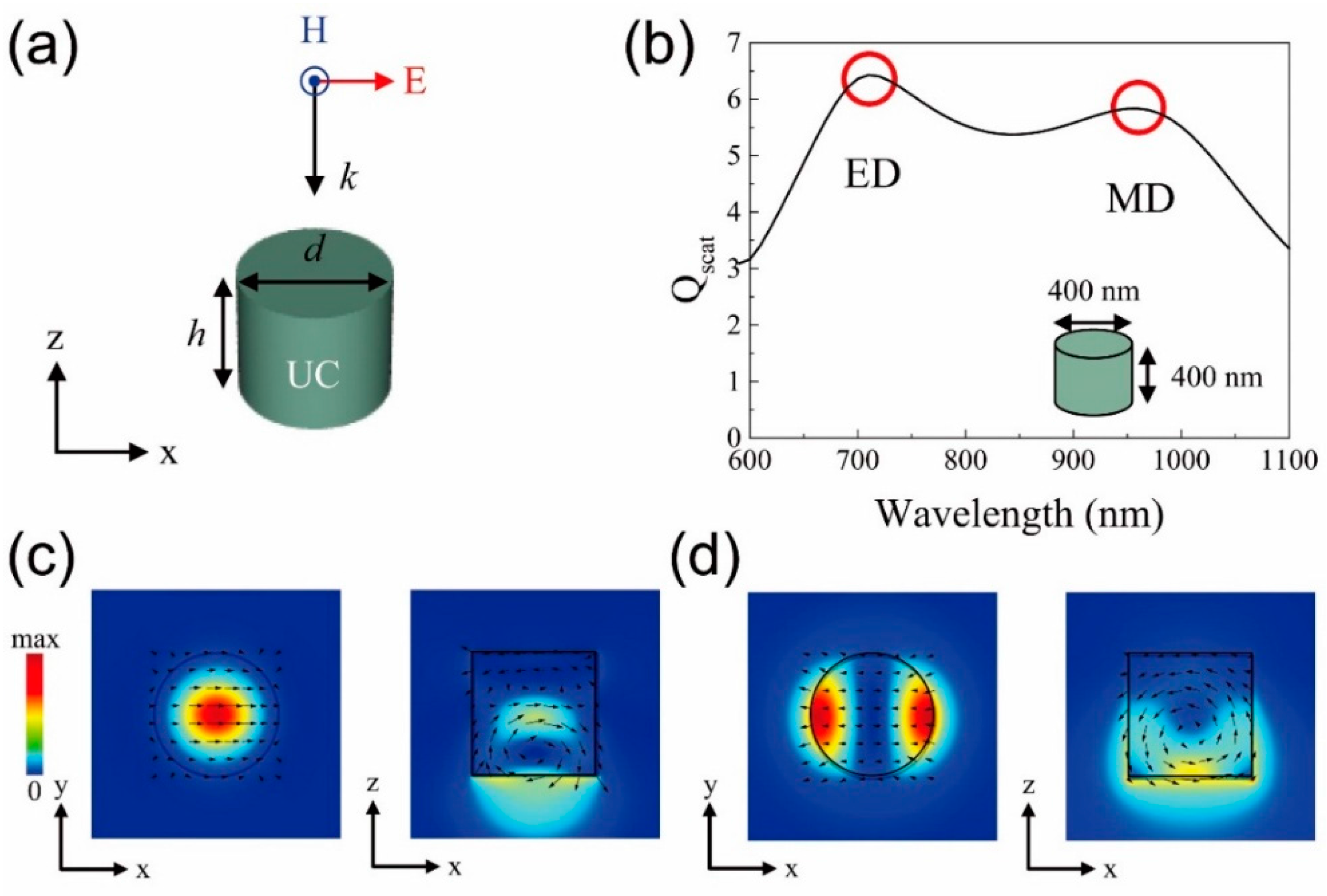
First, we investigate the Mie resonances of a UC nanocylinder by calculating the scattering cross section using a three-dimensional (3D) finite-difference time-domain (FDTD) method. As shown in Figure 1a, incident light with linear polarization along the x-axis (Ex-polarization) propagates along the z-axis and is scattered by a nanocylinder with height h and a diameter d, in which the cylinder is made of the UC material. The UC material was assumed to absorb near-infrared light with a wavelength of 980 nm and emit visible light with a wavelength of 660 nm. Because Er3+ doped KNbO3 has a higher upconversion efficiency at 530–550 nm (green) than at 660 nm (red), we focus on the red UC enhancement so that simultaneous efficient conversion of most of visible colors, green and red, from the NIR light can be realized. In addition, the mechanism to enhance the upconversion to red light by the resonances in an array of nanocylinder can be applied from the UC to green light in same way. For the nanocylinder with h = 400 nm and d = 400 nm, the normalized scattering cross section (Qscat), defined by the ratio between a scattering cross section and a geometrical cross section, is calculated in Figure 1b. First and second resonances are observed as peaks in the graph of Qscat at wavelengths of 710 nm and 960 nm, which correspond to ED and MD, respectively. The electric field intensity profiles and vector plots for the two resonances in Figure 1c,d show that the resonances are ED and MD, respectively. In particular, in the side view, the electric field of the ED near the middle of the cylinder is mainly oriented along the x-axis, which is similar to the Ex dipole. In contrast, the electric field of the MD exhibits a current loop in the nanocylinder as the usual magnetic dipole.
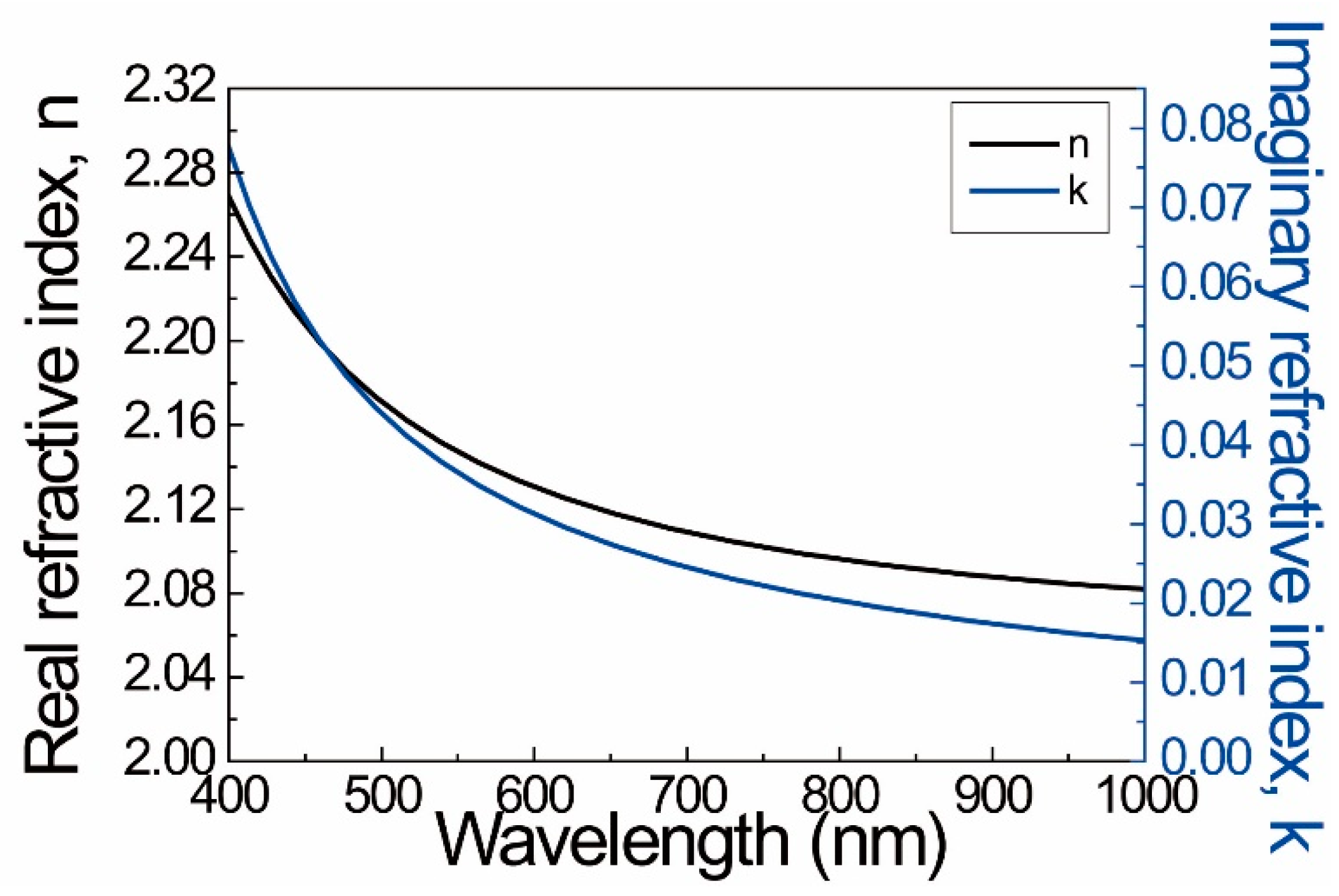
Here, we set the optical properties of the UC material and FDTD conditions as follows. In the simulation, we used Er3+-doped KNbO3 (with the refractive index plotted in the graph of Figure A1) as the UC material. This UC material absorbs 980 nm wavelength light and sequentially emits 660 nm [25,26,27]. The spatial grid of FDTD is 10 nm and the boundary conditions are perfectly matched layers in the single nanocylinder structure and a periodic boundary condition in the array structure. In addition, the gold is fitted as Drude critical points in the model [28].
2.2. Tailoring the Wavelengths of ED and MD Resonances
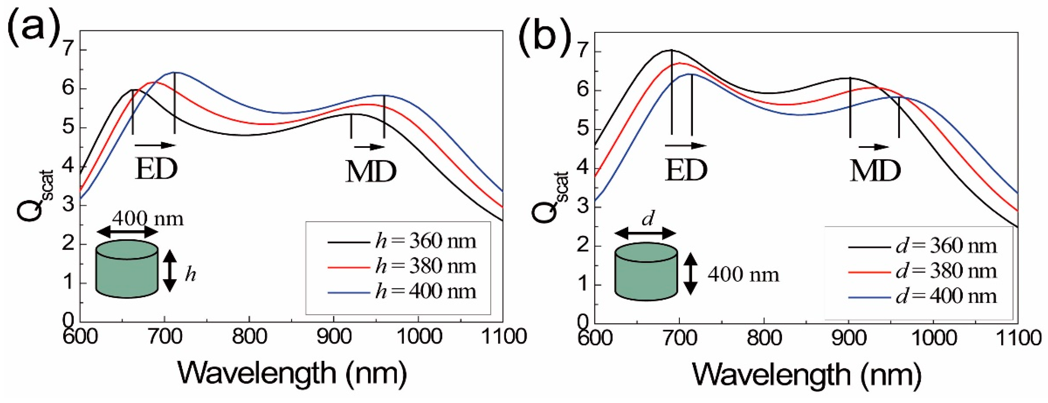
Resonant wavelengths of the Mie resonance in a nanoparticle depend on the geometry and the structure parameters. We calculated the normalized scattering cross section of a single UC nanocylinder to determine the dependences of ED- and MD-resonant wavelengths on the cylinder geometry, i.e., the height (h) and diameter (d), so that the emission and absorption wavelengths of the UC process match those of the ED and MD resonances. Figure 2 shows the Qscat spectrum of single UC nanocylinders with different heights (360 nm, 380 nm, and 400 nm) and a fixed diameter (400 nm), as well as for different diameters (360 nm, 380 nm, and 400 nm) with a fixed height (400 nm). The resonant wavelengths of the ED and MD red-shift as the size of the nanocylinder, i.e., height or diameter, increases. However, the wavelength changes of ED and MD differ depending on if the diameter or height is varied. When the height changes from 360 nm to 400 nm by an amount of 40 nm while the diameter is fixed at 400 nm, the ED wavelength increases by 40 nm, and the wavelength shift of MD is larger at 50 nm. In contrast, when the diameter increases from 360 to 400 nm with a fixed height of 400 nm, the wavelengths of ED and MD increase 30 nm and 60 nm, respectively. Using two different dependencies, the ED and MD resonances are allowed to match with the emission and absorption wavelengths, respectively, of the UC material.
2.3. Periodic Structure of UC Nanocylinders
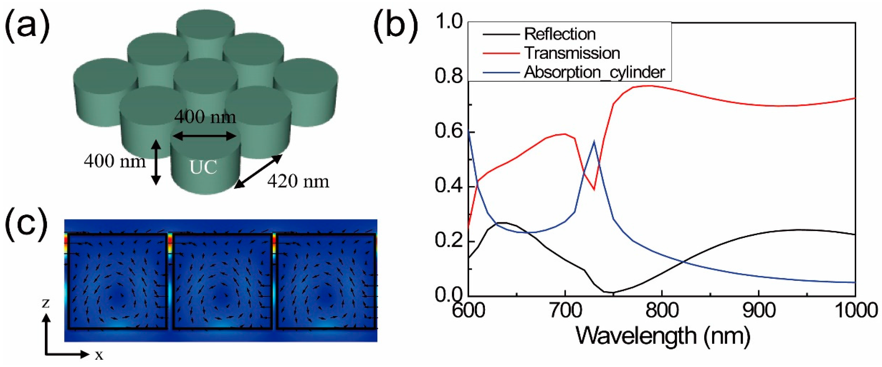
To exploit a UC nanocylinder in a usable device, we consider an array of UC nanocylinders arranged in a square lattice with a period of 420 nm, as shown in Figure 3a. The height and diameter of the nanocylinder are 400 nm and 400 nm, respectively. We calculated the spectra for reflectance, transmittance, and absorbance in the nanocylinder array structure in Figure 3b. The absorbance has a peak of 0.56 at a wavelength of 730 nm. In terms of the wavelength, the electric field vector flows of each nanocylinder are similar to those of the MD of a single nanocylinder (Figure 1d), and the overall vector flows for the entire surface of an array of nanocylinders is directed along the x-direction in phase, as shown in Figure 3c. Magnetic dipole resonance in each nanocylinder and the coupling between cylinders contribute to absorption enhancement. Because of the coupling between cylinders, a concentrated electric field, called an electric hotspot, is induced along the direction of the electric field of the incident lights. We are able to use this MD resonance of a single cylinder and the coupling effect of MDs in an array of nanocylinders by tuning the resonant wavelength of the resonance to the absorption wavelength of the material.
2.4. UC Nanocylinder on a Gold Substrate and an Absorption Enhancement at 980 nm
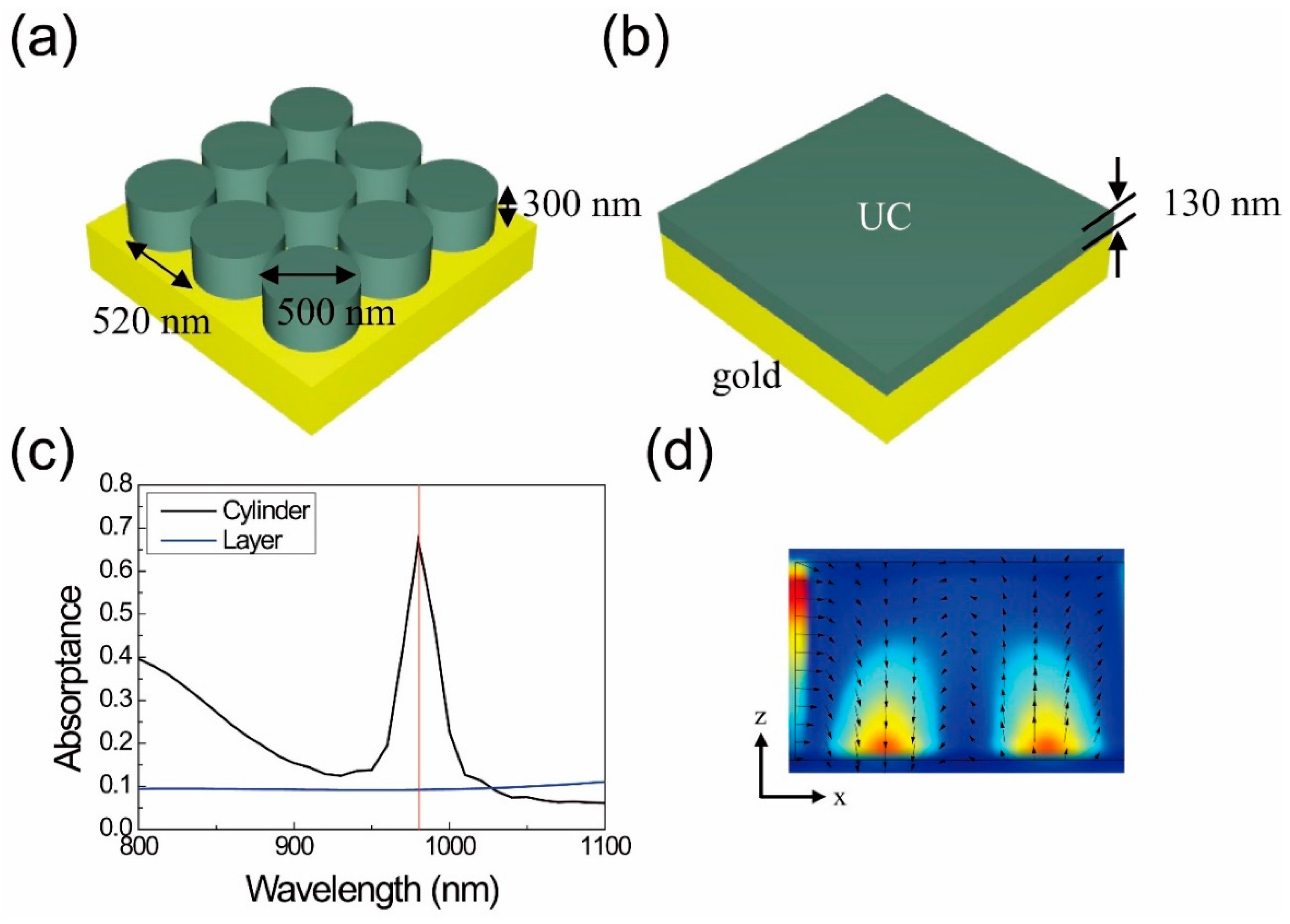
In order to increase the optical path length of the absorbed NIR (near-infrared) light and have uni-directional emission of the converted visible light, we introduce a gold substrate just below the array of nanocylinders, as shown in Figure 4a. The optimized structure has an absorption peak with a wavelength of 980 nm, h = 300 nm, d = 500 nm, and a period of 520 nm. In order to match the absorption peak of the nanocylinder array at the absorption wavelength of UC material, 980 nm, we adjust the period to 520 nm, because the peak wavelength depends on this period. As a reference structure, a thin UC film with a thickness of 130 nm on a gold substrate is assumed in Figure 4b, which has the same volume as the proposed structure. In the absorbance curve of Figure 4c, the reference structure is almost a constant value of 10% in the wavelength range of interest, 800 nm–1100 nm. In contrast, the proposed nanocylinder structure has a sharp absorption peak of 980 nm with an absorbance of 67.1%, which is 7.3 times larger than that (9.2%) of the reference structure. According to the mode profile at 980 nm, as shown in Figure 4d, a strong electric field intensity is observed at the bottom of the nanocylinder on a gold substrate and at the air slots between the nanocylinders. One field enhancement originates from the surface plasmon polaritons (SPPs), as indicated by the field intensity and the field direction normal to the gold substrate. The other enhancements are caused by the electric hotspots due to the coupling of MDs in the nanocylinders. The coupling of two resonances, SPP and electric hotspot, made a sharp absorption peak at 980 nm, which is the absorption wavelength of the UC material.
2.5. Spontaneous Emission Enhancement at 660 nm
Next, in order to investigate the emission properties of the converted visible light with wavelengths of 660 nm, we calculated the spontaneous emission (SE) enhancement of dipole sources in the proposed structure, as seen in Figure 4a, which are horizontally polarized (Ex) or perpendicularly polarized (Ez). SE enhancement is calculated using the following equation: SE enhancement = (emitted power of dipole source in UC nanocylinder)/(emitted power of dipole source in bulk UC material). We put a dipole source with a wavelength of 660 nm inside a UC nanocylinder and measured the total output power of the dipole source by integrating the Poynting vectors outgoing from the nanocylinder. We scanned the position of the dipole source with a spatial resolution of 20 nm. The actual calculation region is set to a quarter of a nanocylinder due to the mirror symmetry of the nanocylinder.
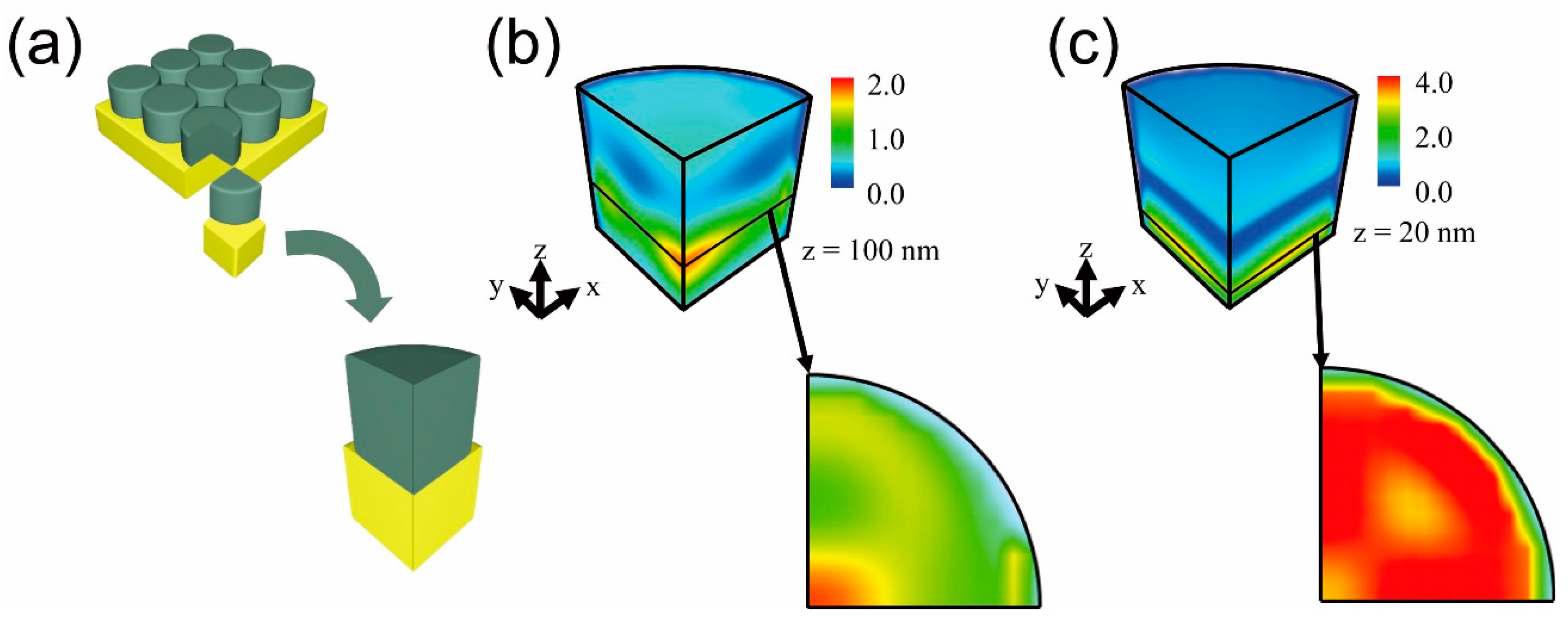
The Ex dipole source, parallel to the gold substrate, has a maximum SE rate enhancement of 2.0 at a plane with z = 100 nm above the substrate, as shown in Figure 5b. Considering an image electric dipole on a gold substrate, which is anti-parallel to the original Ex dipole source, the height of 100 nm corresponds to approximately a quarter wavelength of 660 nm in the UC material, such that the image dipole can constructively interfere with the original dipole [29]. The horizontal mapping of the enhancement is similar to the mode profile of the ED mode (left of Figure 1c), which indicates that the emission of the Ex dipole source is enhanced via the Purcell effect of the ED mode in a nanocylinder [30]. The Ey dipole source has the same spatial distribution as the SE enhancement of the Ex dipole, except for a rotation by 90°.
On the other hand, the Ez dipole source emits light strongly at the surface of the gold substrate, which is shown in Figure 5c. Here, the maximum enhancement position 20 nm above the substrate is limited by the spatial resolution of the scanning (20 nm). If a smaller resolution is applied for the enhancement of the Ez dipole, the maximum enhancement is at nearest position to the gold substrate. The SE rate of the Ez dipole source is enhanced 4.0 times its normal maximum for the plasmonic mode. Finally, we summarize the SE rate enhancements at a visible wavelength of 660 nm, the absorption enhancement at an NIR wavelength of 980 nm for the proposed nanocylinder array structure, and the reference structure in Table 1. The absorption of the nanocylinder structure is 7.3 times larger than that of the reference structure due to the fact it has coupled with the SPPs and the MDs in each nanocylinder.
For the emission of 660 nm, the properties of the SE rate enhancements are very different depending on the direction of the dipole sources. In the case of parallel dipole sources (E‖) such as Ex or Ey dipole sources, the SE rate averaged over the nanocylinder is 0.62 times that of the SE rate in bulk UC material because the SE rate is suppressed near a half wavelength in the UC material [29], which is smaller than that of the reference structure. However, since the useful converted visible light is only the emitted light into free space, which escapes from the UC layer and propagates upward, an output efficiency, ηz, defined as the ratio between the upward-directional emitted power and the total emitter power, should also be considered alongside the SE rate enhancements. The output efficiency is same as the extraction efficiency in light-emitting diodes. The upward emission of the 660 nm wavelength light is ×0.66 the total emitted power from the parallel dipole source in the nanocylinder structure due to constructive interference of the dipole source and the image dipole source on a gold substrate [29]; in contrast, the upward emission in the reference structure is only ×0.11 of the total emitter power. Therefore, combined with the SE rate enhancements and the output efficiency, the effective upward emission of the parallel dipole source in the nanocylinder is 3.8 times larger than the reference structure. Here, the effective upward emission enhancement can be estimated by the ratio of the upward emission in the nanocylinder and the reference, in which the upward emitted power is obtained by the SE rate enhancement multiplied by the output efficiency, ηz. On the other hand, in the case of a perpendicular dipole source (Ez), the SE rate enhancements of the nanocylinder and the reference are similar, ×1.1 and ×1.5, respectively, because of the SPP coupling. However, the output efficiency of the nanocylinder (0.53) is distinct from that of the reference (0.01). In the reference that consists of a UC film on a gold substrate, the Ez dipole source couples with a horizontally propagating SPP wave and the upward emission is strongly suppressed. In contrast, in the nanocylinder array, light from the Ez dipole source is also able to couple to the SPPs, but the coupled SPPs can scatter at the edge of the finite nanocylinder, resulting in a high output efficiency of 0.53. Therefore, the effective upward emission of the perpendicular source in the nanocylinder is 41 times larger than that of the reference due to its strong upward directionality. If two parallel polarized dipole sources, Ex and Ey, and one perpendicularly polarized dipole source, Ez, are equally considered, the total effective upward emission of 660 nm light in the nanocylinder array is 21 times larger than the reference structure. As a result of the emission enhancement (×21) and the absorption enhancement (×7.3), the total effective enhancement of the UC process is ×155 the reference structure due to SPP coupling, coupling between the MD mode, and effective vertical directionality.
3. Conclusions
In this paper, we proposed a dielectric nanostructure made of UC material that converts NIR light into visible light. The resonances in the structure enable the enlargment of the light-matter interactions in both absorption and emission to improve the efficiency of the UC process. The absorption at 980 nm is enhanced by an electric hotspot induced by the MD resonances and surface plasmons at the interface between the nanocylinders and a gold substrate. The absorption is 7.3 times larger than the reference UC film structure. In addition, we obtain the enhanced upward emission of 660 nm wavelength light by directional scattering of the emission light due to constructive interference and scattering of the nanocylinders. The upward emission rates are 21 times larger than those of the reference structure. In total, the efficiency of the wavelength conversion combined with the absorption and emission rates is improved by a factor of 155. The converted light can be used effectively because the direction of the emitted light is upward. As a result, the efficiency of devices that use UC materials (such as solar cells and sensors) can be significantly improved.
A KNbO3 thin film can be deposited on the silicon substrate using the polymeric precursor method (Pechini method) [31]. Gold thicker than several hundred nanometers is deposited on the KNbO3 film. Then, the sample is flipped and bonded to the other substrate. The original silicon substrate is removed by wet etching and the KNbO3 film on gold layer is obtained. The next process to form an array of nanocylinders can be performed by using conventional electron-beam lithography or nanostamp techniques.
Because the exciting electric field distribution in the absorption at 980 nm is spatially localized due to the resonance effects, as shown in Figure 4, the spontaneous emission enhancement can be affected by the spatial distribution of the absorption like in the case of lasing in nanocavity [32]. However, in order to consider the distribution adequately, there are several complicated factors to be considered such as the three-dimensional (3D) dynamics of carriers and photons in the multilevel system of a UC nanocylinder, carrier diffusion velocities, energy transfer rates in the UC process, and the 3D distribution of photon densities, which should be analyzed in a further study. Our analysis of the SE enhancements assumes that the 980 nm absorption generates the corresponding carriers in a nanocylinder uniformly, which can provide a reasonable value of the SE enhancements as long as the diffusion velocities are large enough compared to the size of a nanocylinder, 500 nm.
Enhancements of the UC process by using nanostructures have been reported in other UC materials such as ZnO/Zn [33] and InAs quantum dots (QDs) [34]. In ZnO/Zn, the nanostructure made by femtosecond laser ablation enhances the UC process from 800 nm to 500 nm, with an enhancement factor of one order of magnitude. In InAs QDs, the flat bandedge property of a photonic crystal waveguide enhances the UC process, achieving lasing of 1.3 mm light from the absorption of 1.55 mm light. In contrast to such UC nanostructures that have small effective UC conversion areas of several micrometers, our UC nanocylinder array made by the lanthanide UC material can be fabricated on a wafer scale by nanostamp or nanosphere lithography techniques; thereby, the UC process increases by two orders of magnitude.
Acknowledgments
This work was supported in part by the National Research Foundation of Korea through the Korean Government under grant NRF-2013M3C1A3065051, NRF-2015R1A2A1A15055998, and NRF-2016R1C1B2007007.
Author Contributions
Kihwan Moon performed simulations and wrote the manuscript. Young Jin Lee and Seokhyeon Hong designed structures and performed simulations. Soon-Hong Kwon supervised all simulations and revised the manuscript.
Conflicts of Interest
The authors declare no conflict of interest.
Appendix A
Figure A1.
The experimentally measured refractive index (real: black; imaginary: blue) of the UC material, Er3+-doped KNbO3.
Figure A1.
The experimentally measured refractive index (real: black; imaginary: blue) of the UC material, Er3+-doped KNbO3.

References
- Menyuk, N.; Dwight, K.; Pierce, J.W. NaYF4: Yb,Er—An efficient upconversion phosphor. Appl. Phys. Lett. 1972, 21, 159. [Google Scholar] [CrossRef]
- Yi, G.S.; Chow, G.M. Synthesis of hexagonal-phase NaYF4:Yb,Er and NaYF4:Yb,Tm nanocrystals with efficient up-conversion fluorescence. Adv. Funct. Mater. 2006, 16, 2324–2329. [Google Scholar] [CrossRef]
- Van Sark, W.G.J.H.M.; de Wold, J.; Rath, J.K.; Meijerink, A.; Schropp, R.E.I. Upconversion in solar cells. Nanoscale Res. Lett. 2013, 8, 81. [Google Scholar] [CrossRef] [PubMed]
- Cheng, Y.Y.; Fuckel, B.; MacQueen, R.W.; Khoury, T.; Clady, R.G.C.R.; Schylze, T.F.; Ekins-Daukes, N.J.; Crossley, M.J.; Stannowski, B.; Lips, K.; et al. Improving the light-harvesting of amorphous silicon solar cells with photochemical upconversion. Energy Environ. Sci. 2012, 5, 6953–6959. [Google Scholar] [CrossRef]
- Ramachari, D.; Esparza, D.; Lopez-Luke, T.; Romero, V.H.; Perez-Mayen, L.; De la Rosa, E.; Jayasankar, C.K. Synthesis of co-doped Yb3+-Er3+:ZrO2 upconversion nanoparticles and their applications in enhanced photovoltaic properties of quantum dot sensitized solar cells. J. Alloys Compd. 2017, 698, 433–441. [Google Scholar] [CrossRef]
- Yu, J.; Yang, Y.L.; Fan, R.Q.; Wang, P.; Dong, Y.W. Enhanced photovoltaic performance of dye-sensitized solar cells using a new photoelectrode material: Upconversion YbF3-Ho/TiO2 nanoheterostructures. Nanoscale 2016, 8, 4173–4180. [Google Scholar] [CrossRef] [PubMed]
- Nyk, M.; Kumar, R.; Ohulchanskyy, T.Y.; Bergey, E.J.; Prasad, P.N. High Contrast in Vitro and in Vivo Photoluminescence Bioimaging Using Near Infrared to Near Infrared Up-Conversion in TM3+ and Yb3+ Doped Fluoride. Nano Lett. 2008, 8, 3834–3838. [Google Scholar] [CrossRef] [PubMed]
- Xiong, L.Q.; Chen, Z.G.; Yu, M.X.; Li, F.Y.; Liu, C.; Huang, C.H. Synthesis, characterization, and in vivo targeted imaging of amine-functionalized rare-earth up-converting nanophosphors. Biomaterials 2009, 30, 5592–5600. [Google Scholar] [CrossRef] [PubMed]
- Lin, H.; Jiang, S.B.; Wu, J.F.; Song, F.; Peyghambarian, N.; Pun, E.Y.B. Er3+ doped Na2O-Nb2O5-TeO2 glasses for optical waveguide laser and amplifier. J. Phys. D Appl. Phys. 2003, 36, 812–817. [Google Scholar] [CrossRef]
- Singh, S.K.; Kumar, K.; Rai, S.B. Diode laser pumped Gd2O3:Er3+/Yb3+ phosphor as optical nano-heater. Appl. Phys. B 2010, 100, 443–446. [Google Scholar] [CrossRef]
- Shalav, A.; Richards, B.S.; Trupke, T.; Kramer, K.W.; Gudel, H.U. Application of NaYF4: Er3+ up-converting phosphors for enhanced near-infrared silicon solar cell response. Appl. Phys. Lett. 2005, 86, 013505. [Google Scholar] [CrossRef]
- Lee, G.Y.; Jung, K.; Jang, H.S.; Kyhm, J.; Han, I.K.; Park, B.; Ju, H.; Kwon, S.J.; Ko, H. Upconversion luminescence enhancement in plasmonic architecture with random assembly of metal nanodomes. Nanocsale 2016, 8, 2071–2080. [Google Scholar] [CrossRef] [PubMed]
- Park, K.; Jung, K.; Kwon, S.J.; Jang, H.S.; Byun, D.; Han, I.K.; Ko, H. Plasmonic nanowire-enhanced upconversion luminescence for anticounterfeit Devices. Adv. Funct. Mater. 2016, 26, 7836–7846. [Google Scholar] [CrossRef]
- Guo, K.M.; Li, M.Y.; Fang, X.L.; Liu, X.L.; Zhu, Y.D.; Hu, Z.Q.; Zhao, X.Z. Enhancement of properties of dye-sensitized solar cells by surface plasmon resonance of Ag nanowire core-shell structure in TiO2 films. J. Mater. Chem. A 2013, 1, 7229–7234. [Google Scholar] [CrossRef]
- Nam, M.; Kwon, N.-K.; Kwon, S.J.; Kwon, S.-H.; Cha, M.; Lee, S.-H.; Park, S.; Jeong, D.; Lee, K.-T.; Rhee, H.; et al. Multi-Functional Transparent Luminescent Configurationfor Advanced Photovoltaics. Adv. Energy Mater. 2016, 6, 1502404. [Google Scholar] [CrossRef]
- Bezares, F.J.; Long, J.P.; Glembocki, O.J.; Guo, J.P.; Rendell, R.W.; Kasica, R.; Shirey, L.; Owrutsky, J.C.; Caldwell, J.D. Mie resonance-enhanced light absorption in periodic silicon nanopillar arrays. Opt. Express 2013, 21, 27587–27601. [Google Scholar] [CrossRef] [PubMed]
- Liu, X.M.; Zhao, Q.; Lan, C.W.; Zhou, J. Isotropic Mie resonance-based metamaterial perfect absorber. Appl. Phys. Lett. 2013, 103, 031910. [Google Scholar] [CrossRef]
- Callewaert, F.; Chen, S.; Butun, S.; Aydin, K. Narrow band absorber based on a dielectric nanodisk array on silver film. J. Opt. 2016, 18, 075006. [Google Scholar] [CrossRef]
- Hong, S.; Lee, Y.J.; Moon, K.; Kwon, S.H. Double resonance perfect absorption in a dielectric nanoparticle array. Curr. Opt. Photonics 2017, 1, 228–232. [Google Scholar] [CrossRef]
- Cheng, J.R.; Ansari-Oghol-Beig, D.; Mosallaei, H. Wave manipulation with designer dielectric metasurfaces. Opt. Lett. 2014, 39, 6285–6288. [Google Scholar] [CrossRef] [PubMed]
- Gaillot, D.P.; Croenne, C.; Zhang, F.; Lippens, D. Transformation optics for the full dielectric electromagnetic cloak and metal-dielectric planar hyperlens. New J. Phys. 2008, 10, 115039. [Google Scholar] [CrossRef]
- Moitra, P.; Slovick, B.A.; Li, W.; Kraychencko, I.I.; Briggs, D.P.; Krishnamurthy, S.; Valentine, J. Large-scale all-dielectric metamaterial perfect reflectors. ACS Photonics 2015, 2, 692–698. [Google Scholar] [CrossRef]
- Moitra, P.; Slovick, B.A.; Yu, Z.G.; Krishnamurthy, S.; Valentine, J. Experimental demonstration of a broadband all-dielectric metamaterial perfect reflector. Appl. Phys. Lett. 2014, 104, 171102. [Google Scholar] [CrossRef]
- Slovick, B.; Yu, Z.G.; Berding, M.; Krishnamurthy, S. Perfect dielectric-metamaterial reflector. Phys. Rev. B 2013, 88, 165116. [Google Scholar] [CrossRef]
- Sun, S.Y.; Ge, Y.Y.; Zhao, Y.J.; Yuan, X.Y.; Zhao, Y.Z.; Zhou, H.P. Up-conversion luminescence behaviors in Er3+ doped single crystal KNbO3 nanosheets. RSC Adv. 2016, 6, 113038–113044. [Google Scholar] [CrossRef]
- Balakrishnaiah, R.; Kim, D.W.; Yi, S.S.; Kim, K.D.; Kim, S.H.; Jang, K.W.; Lee, H.S.; Jeong, J.H. Frequency upconversion fluorescence studies of Er3+/Yb3+-codoped KNbO3 phosphors. Thin Solid Films 2009, 517, 4138–4142. [Google Scholar] [CrossRef]
- Wang, Y.L.; Wang, L.H.; Zhao, Y.J.; Yan, D. Improved luminescence behavior in Er3+ doped KNbO3 perovskite structure ceramics. Ceram. Int. 2016, 42, 17911–17915. [Google Scholar] [CrossRef]
- Johnson, P.B.; Christy, R.W. Optical constants of the noble metals. Phys. Rev. B 1972, 6, 4370. [Google Scholar] [CrossRef]
- Ee, H.S.; Kim, S.K.; Kwon, S.H.; Park, H.G. Design of polarization-selective light emitters using one-dimensional metal grating mirror. Opt. Express 2011, 19, 1609–1616. [Google Scholar] [CrossRef] [PubMed]
- Purcell, E.M.; Torrey, H.C.; Pound, R.V. Resonance absorption by nuclear magnetic moments in a solid. Phys. Rev. 1946, 69, 37. [Google Scholar] [CrossRef]
- Simoes, A.Z.; Ries, A.; Riccardi, C.S.; Gonzalez, A.H.; Zaghete, M.A.; Stojanovic, B.D.; Cilense, M.; Varela, J.A. Potassium niobate thin films prepared through polymeric precursor method. Mater. Lett. 2004, 58, 2537–2540. [Google Scholar] [CrossRef]
- Nozaki, K.; Baba, T. Carrier and photon analyses of photonic microlasers by two-dimensional rate equations. IEEE J. Sel. Areas Commun. 2005, 23, 1411–1417. [Google Scholar] [CrossRef]
- Li, H.; Zhang, C.-Y.; Li, X.-F.; Xiang, J.; Tie, S.-L.; Lan, S. Enhanced upconversion luminescence from ZnO/Zn hybrid nanostructures induced on a Zn foil by femtosecond laser ablation. Opt. Express 2015, 23, 30118–30126. [Google Scholar] [CrossRef] [PubMed]
- Oda, H.; Yamanaka, A.; Ozaki, N.; Ikeda, N.; Sugimoto, Y. Operation of an InAs quantum-dot embedded GaAs photonic crystal slab waveguide laser by using two-photon pumping for photonics integrated circuits. AIP Adv. 2016, 6, 065215. [Google Scholar] [CrossRef]
Figure 1.
(a) A nanocylinder with height h and diameter d created using an upconversion material (UC). Incident light with a linearly polarized electric field along the x-axis propagating along the z-axis; (b) normalized scattering cross section (Qscat) of a UC nanocylinder with h = 400 nm and d = 400 nm. Resonant wavelengths of the electric dipole (ED) and magnetic dipole (MD) are 710 nm and 960 nm, respectively. Top and side views of the electric field intensity profiles and vector field distributions for (c) ED (710 nm) and (d) MD (960 nm). The top views are obtained from directly above the center of the nanocylinder.

Figure 2.
Normalized scattering cross section (Qscat) as a function of wavelength for a nanocylinder with (a) a fixed diameter (d) of 400 nm and different heights (h) of 360 nm, 380 nm, and 400 nm; and (b) a fixed height (h) of 400 nm and different diameters (d) of 360 nm, 380 nm, and 400 nm. The resonant wavelengths of ED and MD increase with increasing h and d.

Figure 3.
(a) Array of UC nanocylinders arranged in a square lattice with a period of 420 nm. The cylinder has a height of 400 nm and a diameter of 400 nm; (b) Reflection (black), transmission (red), and absorption curves (blue) as a function of wavelength; (c) Electric field intensity profile with a vector field plot in the side view.

Figure 4.
(a) Schematic of the proposed UC nanocylinder array structure with a gold substrate. Here, the UC cylinders have a height of 300 nm and a diameter of 500 nm. The period in the array is 520 nm; (b) Reference structure consisting of a UC film with a thickness of 130 nm and a gold substrate. The thickness is determined to have the same UC volume as the proposed nanocylinder array; (c) The absorptances of the proposed structure (black) and reference structure (blue) as functions of wavelength. The absorptance of a cylinder array is 67.1% at 980 nm; (d) The electric field intensity profile with a vector field plot of the UC cylinder array.

Figure 5.
(a) A schematic diagram of one quarter of a UC nanocylinder to calculate the spontaneous emission (SE) enhancement mapping. The cylinder has a height of 300 nm and a diameter of 500 nm. The period in the array is 520 nm. SE enhancement distributions of (b) Ex and (c) Ez dipole sources; a magnified top view represents the horizontal SE enhancement mapping obtained at a plane with z = 100 nm in the case of the Ex dipole source and a plane with z = 20 nm in the case of the Ez dipole source, respectively. A plane with z = 0 nm represents the interface between the nanocylinder and gold substrate.


Table 1.
The volume average spontaneous emission (SE) enhancements of parallel (E‖) and perpendicular (Ez) dipole sources at a wavelength of 660 nm and the absorption enhancement at a wavelength of 980 nm. The UC material absorbs near-infrared (NIR) light with a wavelength of 980 nm and emits visible light with a wavelength of 660 nm. SE enhancements in an array of nanocylinders on a gold substrate and those in the reference structure are compared. SE enhancements in Table 1, the averaged SE enhancements, are calculated by integrating the values over the whole nanocylinder volume. The output efficiency ηz is defined as the ratio between the upward-directional emitted power and the total emitter power.
| Cylinder (h 300_d 500) | Reference | |||||
|---|---|---|---|---|---|---|
| SE Enhancement | ηz | SE Enhancement | ηz | |||
| E‖ | 0.62 | 0.66 | 1.0 | 0.11 | 3.8 | 7.3 |
| Ez | 1.1 | 0.53 | 1.5 | 0.01 | 41 | |
© 2017 by the authors. Licensee MDPI, Basel, Switzerland. This article is an open access article distributed under the terms and conditions of the Creative Commons Attribution (CC BY) license (http://creativecommons.org/licenses/by/4.0/).
Share and Cite
MDPI and ACS Style
Moon, K.; Lee, Y.J.; Hong, S.; Kwon, S.-H. Wavelength Conversion Enhancement Achieved by Using Resonance in an Array of Nanocylinders. Appl. Sci. 2017, 7, 1246. https://doi.org/10.3390/app7121246
AMA Style
Moon K, Lee YJ, Hong S, Kwon S-H. Wavelength Conversion Enhancement Achieved by Using Resonance in an Array of Nanocylinders. Applied Sciences. 2017; 7(12):1246. https://doi.org/10.3390/app7121246
Chicago/Turabian StyleMoon, Kihwan, Young Jin Lee, Seokhyeon Hong, and Soon-Hong Kwon. 2017. "Wavelength Conversion Enhancement Achieved by Using Resonance in an Array of Nanocylinders" Applied Sciences 7, no. 12: 1246. https://doi.org/10.3390/app7121246
Note that from the first issue of 2016, this journal uses article numbers instead of page numbers. See further details here.