A New Compact Octagonal Shape Perfect Metamaterial Absorber for Microwave Applications
by
 , and
, and
Mohammad Jakir Hossain
1,*, 
Mohammad Rashed Iqbal Faruque
1,*,
Mohammad Tariqul Islam
2,* and
Kamarulzaman Bin Mat
2,* 1
Space Science Centre (ANGKASA), Institute of Climate Change (IPI), Universiti Kebangsaan Malaysia, Bangi 43600, Selangor, Malaysia
2
Department of Electrical Electronic and Systems Engineering, Universiti Kebangsaan Malaysia, Bangi 43600, Selangor, Malaysia
*
Authors to whom correspondence should be addressed.
Appl. Sci. 2017, 7(12), 1263; https://doi.org/10.3390/app7121263
Submission received: 31 October 2017
/
Revised: 22 November 2017
/
Accepted: 29 November 2017
/
Published: 6 December 2017
(This article belongs to the Section Acoustics and Vibrations)
Abstract
:A new compact octagonal shape perfect metamaterial absorber (PMA) design, numerical simulation, fabrication, and investigational verification of unit cell that is based on a simple structure are presented in this paper. The suggested structure comprised of three layers, in which interact to produce the plasmonic resonances. The finite-integration technique (FIT) based Computer Simulation Technology (CST) microwave electromagnetic simulator was utilized to examine the design parameters and conduct absorption analysis. The design structure exhibited peak absorption values as 99.64% and 99.95% at frequencies 8.08 GHz and 11.41 GHz, respectively. The absorption characteristics were analysed using the polarization angle of the structure, layer thickness, PMA with resistive load, and number of rings. An N5227A vector network analyser was used for the measurement. The measured results of the fabricated prototype were in good agreement with the simulation results. The suggested perfect absorber structure enables innumerable application aimed at X-band for applications like, defence, security, and stealth technology.
1. Introduction
Artificial metamaterials (MMs) are engineered composites consisting of sub-wavelength metallic structures in a host dielectric medium, which are engineered to obtain unconventional properties that are not found naturally. Due to the unconventional electromagnetic properties of numerous metamaterials, namely the (-) ve permittivity, (-) ve permeability, (-) ve refractive index, and invisibility, the design and application of MMs has gained the priority of vigorous research [1,2]. Nevertheless, MMs are also being extensively studied for different applications, for instance, perfect absorbers through the wide electromagnetic spectrum from millimetre to nanometre wavelengths [3,4], multiband absorber [5], polarization insensitive absorber [6], imagers and detectors [7,8], and broad band absorber [9], smart antenna, and beam shaping devices [10,11]. A 24 × 24 mm2 Jerusalem cross with meandered load absorber depicts absorptions of more than 95% at 14.75 GHz and 16.1 GHz [12]. Lin et al. recommended a metamaterial unit cell structure with 10.92 × 10 mm2 dimension that was applicable in microwave regime. The absorption peak of the structure was 96.5%, 96.8%, and 99.6% at 2.15 GHz, 2.28 GHz, and 2.38 GHz, respectively [13]. Zhao et al. offered 10 × 10 mm2 ultra broadband perfect absorber based on an electric split-ring resonator (ESRR) loaded with lumped resistors. The design structure displayed the absorption of 99.3%, 97.1%, and 98.6% at 5.45 GHz, 15.46 GHz, and 19.48 GHz, respectively [14]. Dincer et al. [15] suggested the design for an absorbing metamaterial element with a near unity absorbance. They designed, fabricated, characterized, and analysed a metamaterial absorber (MA) with an absorbance of around 99.99% at 5.48 GHz and 99.92% at 0.865 THz. However, the dimension of the unit cell structure was 36 × 36 mm2. Hossain et al. recommended a design structure of 12 × 12 mm2 composite double negative metamaterial for multi-band operation and reported effective medium ratio was 7.44 [16]. On the other hand, the above author analysed double negative characteristics and compactness, but absorption properties were not analysed in their study. Islam et al. [17] proposed multi-band split S-shaped metamaterial structure for absorption analysis, whereas authors obtained maximum 55% absorption. Kim et al. proposed a dual-band multilayer metamaterial absorber in the megahertz region, which were absorptions of 96% in the 4.0–6.0 GHz range because of the irregular thickness of the resistive sheets [18]. A multi-band perfect metamaterial absorber based on spiral showed the absorption of 99.4%, 96.7%, and 99.1% at three resonant frequencies 9.86 GHz, 12.24 GHz, and 15.34 GHz, simultaneously [5]. Wen et al. suggested a dual-band metamaterial absorber in the terahertz area, which was two discrete absorptions of 80.8% and 63.4% near 0.45 and 0.92 THz [19]. A dual-band MA design, fabrication, and characterization was offered by Tao et al. [20]. Their MA exhibited absorption peaks of 85% and 94% at 1.4 THz and 3.0 THz, respectively. Polarization-independent MAs proposed by Kollatou et al. that performed in the microwave regime. The maximum absorption value was 95.81% at 10.31 GHz [21].
In this paper, compact octagonal shape perfect metamaterial absorber exhibits dual resonance at X-band. The absorption has been changed by altering the polarization angle of unit cell, thickness of substrate and metallic materials, number of rings, and resistive load. Moreover, the size of the proposed unit cell is 10 × 10 mm2, which is physically smaller than the stated metamaterials unit cells in literature [12,13,15,17,22,23,24]. Moreover, the design structure provides high absorption peaks of 99.64% at 8.08 GHz and 99.95% at 11.41 GHz, respectively. It is observed that the absorption of the proposed design is better than the suggested metamaterials unit cells in [12,13,14,17,18,19,20,21,22,23,24,25]. To determine the absorption parameters, the Computer Simulation Technology (CST) microwave studio suite simulator 2015 is used.
2. Design, Numerical Simulation, and Experiment
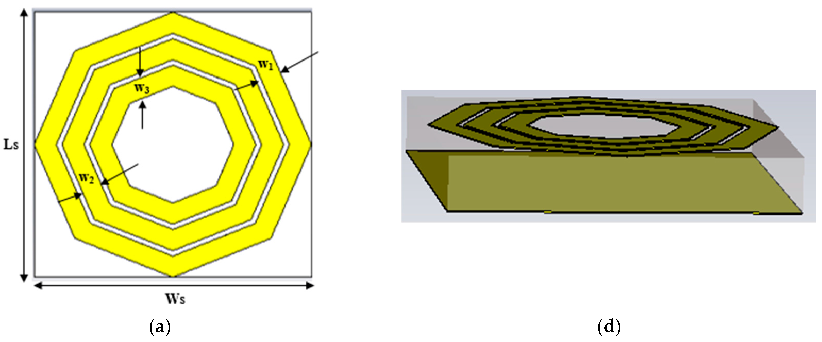
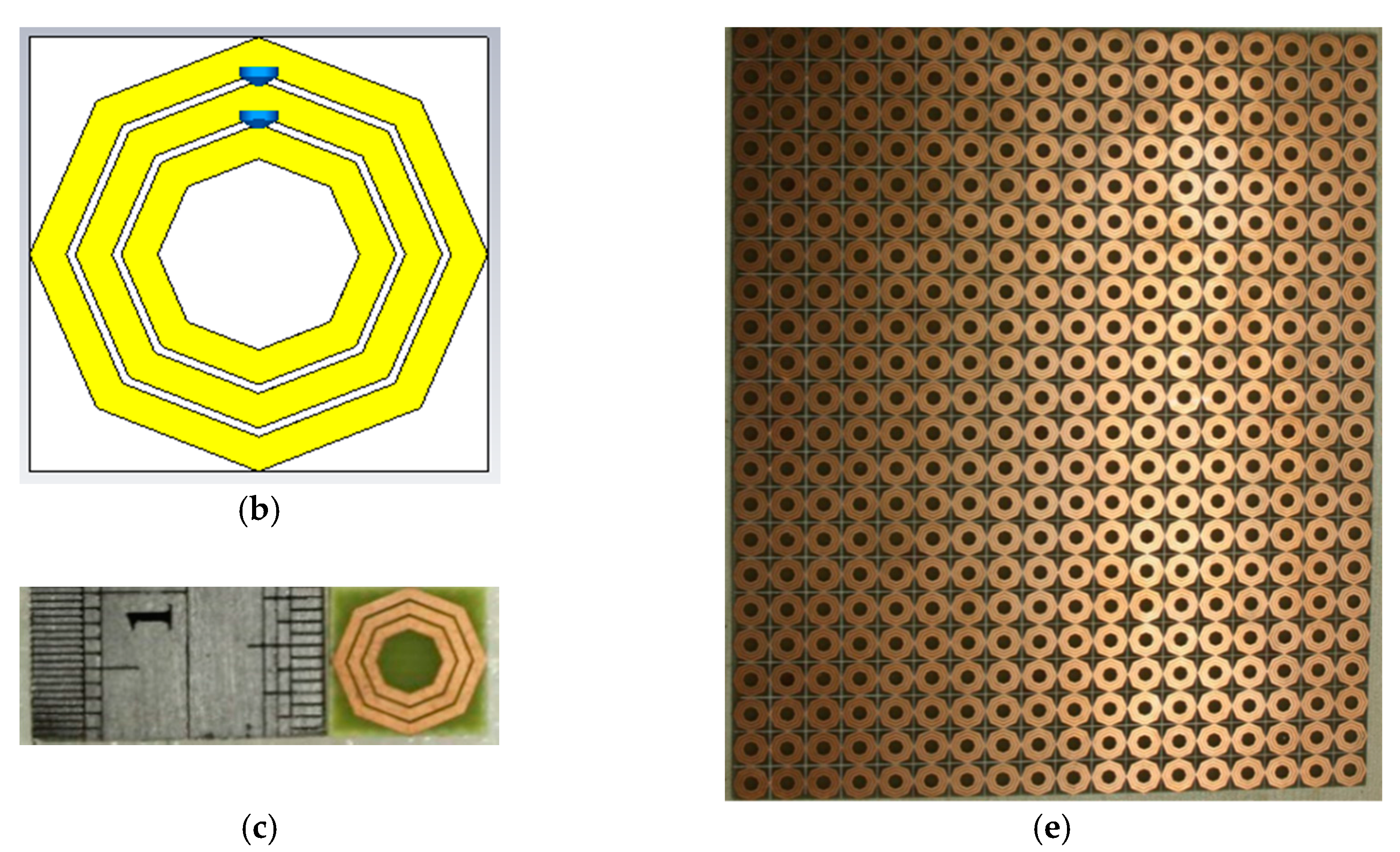
The proposed perfect metamaterial absorber (PMA) consists of three octagonal shape resonators on the dielectric material and a ground plane backside. The proposed perfect metamaterial absorber structure and structural parameters are shown in Figure 1. All of the metallic elements of the PMA are made of copper with a conductivity of 5.8 × 10⁷ S/m and the thickness of copper resonators are 35 µm that are printed on a substrate with standard relative permittivity ε = 4.3, as well as loss tangent δ = 0.025. The parameters of the structure are Ls = 10 mm, Ws = 10 mm, W1 = W2 = W3 = 0.8 mm. The double-sided copper laminated PCB (Printed Circuit Board) (Shenzhen Zhongxinhua Electronics Co., Ltd., Shenzhen, China) is available in the market. Using LPKF S63 PCB prototyping machine (LPKF Laser & Electronics, Tualatin, OR, USA) or chemical process, it is easy to fabricate the design structure. Low cost, high efficient flame retardant4 (FR4) epoxy dielectric material (Shenzhen Zhongxinhua Electronics Co., Ltd., Shenzhen, China) was utilized as substrate material.
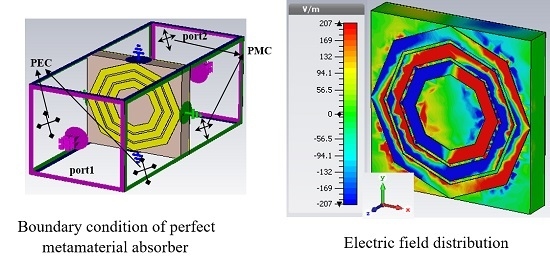
Finite-integration technique (FIT) based CST microwave studio suite simulator has been implemented to examine this design structure in this paper. The electric field and magnetic field have been polarized along the x-axis and the y-axis, respectively, thus wave propagation is along the z-axis. The boundary conditions of perfect magnetic conductor (PEC) and the perfect electric conductor (PMC) are utilized along the x-axis and y-axis, individually, and two waveguide ports are placed on the positive and negative z-axis. In addition, the periodic boundary conditions with the waveguide ports are used in simulation. The schematic drawing of the proposed structure, unit cell with resistive load, fabricated unit cell, side view of the unit cell, and array of the structure are demonstrated in Figure 1.
CST based frequency domain solver was used to determine the reflection coefficient in simulation at 1001 frequency samples. The boundary condition and measurement set up are shown in Figure 2. The fabricated sample encloses 18 × 22 arrays of the structure of copper materials, and the dimension of the fabricated sample are 180 × 220 mm2. The measurement has been performed with two waveguides in the free-space environment. The scattering parameters have been measured by the PNA network analyser (N5227, Agilent Technologies Sdn. Bhd., Petaling Jaya, Malaysia) where the frequency range of the device was 10 MHz–67 GHz. In addition, a calibration kit (Agilent N4694-60001, Agilent Technologies Sdn. Bhd., Petaling Jaya, Malaysia) was utilized to calibrate the network analyser. For that reason, the measurements were completed precisely. The absorption of the design structure is determined using the following equation, A (ω) = 1 − R (ω) − T (ω), where T (ω), R (ω), and A (ω) are the transmittance, reflectance, and absorption at angular frequency ω, respectively. Absorption depends on the scattering parameters, for instance, |S21|2 = T (ω), and |S11|2 = R (ω). The absorption of the incidence electromagnetic (EM) wave is simplified as A (ω) = 1 − R (ω), because back side copper plane blocks the transmission of EM wave. Nonetheless, from the absorption equation, it can be seen that minimizing scattering parameters, which can maximize the absorption of the metamaterials.
3. Results and Discussions
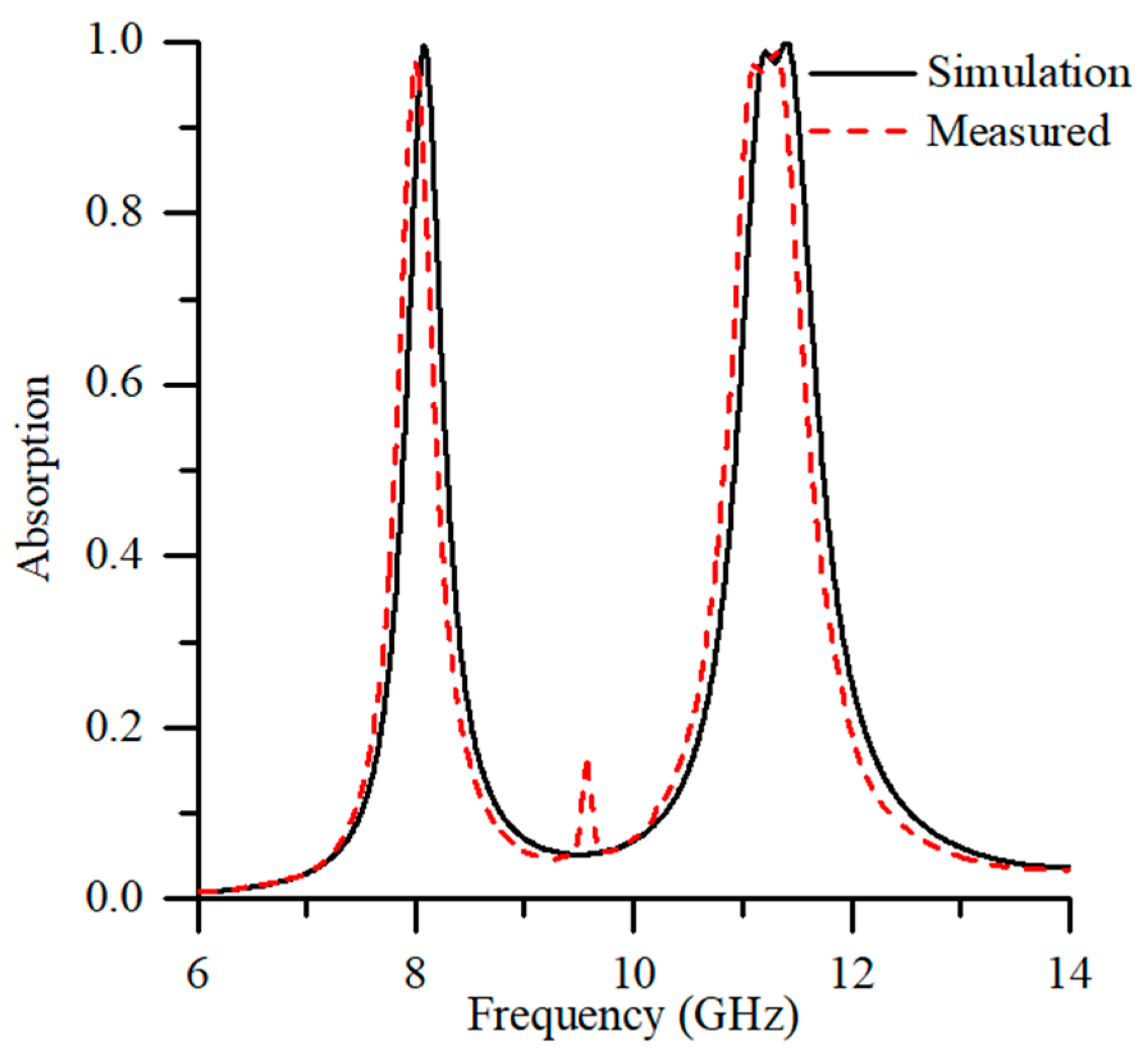
The simulations of the unit cell structure and array structure are executed using a full-wave frequency domain solver based on the FIT. In simulation, the waveguide port with periodic boundary conditions is applied. In this paper, scattering parameters, absorption of design structure with angular rotation, thickness of substrate materials, thickness of radiated patch and ground materials, effect of the resonator’s number, and resistive load have been analysed. The numerical simulation and experimental result of compact octagonal shape PMA has been presented. The numerical simulation and measured absorption A (ω) of the design structure has been demonstrated in Figure 3. As is seen from Figure 3, the frequencies of the proposed design are in X-band.
From Figure 3, the numerical simulation and experimental results are showing agreement with each other. The measured results have been shown the same band when comparing with numerical results in Figure 3. In simulation, the absorption values of the structure are 99.64% and 99.95% at frequencies 8.08 GHz and 11.41 GHz, respectively. However, the values of the absorption are 97.74% at 8.00 GHz, and 98.97% at 11.30 GHz, correspondingly by measurement. Furthermore, the absorption parameter of measured results has been slightly shifted towards the lower frequency and decrease small amount of the magnitude when comparing with simulation results. The small difference can be attributed to fabrication tolerance and open-space measurement procedure.
The electric field and magnetic field distributions are examined at the resonant frequency of 8.08 GHz to understand the physical mechanism of operation. The field distributions are shown in Figure 4. It is observed that there is high concentration of electric field around the outer side of the rings. The electric field are powerfully coupled with the rings and produce electric response that works as like an electric dipole moment. Hence, the charges of outer surface excite along the external electric field. As a result, a magnetic dipole is induced and it produces a magnetic response that makes a resonant absorption. In addition, high concentration of magnetic field is observed around the upper side and lower side of middle rings. The magnetic fields are strongly coupled with the rings and induce magnetic response that works as like a magnetic dipole moment. Consequently, an electric dipole is induced and produces an electric response that makes a resonant absorption. However, the desired response of electric and magnetic fields occur at this resonant frequency concurrently, resulting in almost complete absorption of the EM wave under the ideal condition (Z (ω) = Z0 (ω)).
Therefore, the energy of EM is dissipated in the structure, which produces zero transmission and reflection with unity absorption. Moreover, properties are also observed for the second resonance found at 11.41 GHz suppose its approach, as shown in Figure 5. It is seen from Figure 5, the highest concentration of electric filed occurs at the right side of the octagonal resonator. The non-uniform perturbation of field distribution is also investigated. It indicates that the response of electric and magnetic field are similar to 8.08 GHz response with higher intensity. Hence, this approach is higher than the previous one. Hence, this produces higher absorption rate than 8.08 GHz.
3.1. Analysis of Design Structure with Polarization Angle
The numerical results of compact octagonal shape PMA have been presented. The absorption A (ω) of the design structure has been illustrated in Figure 6.
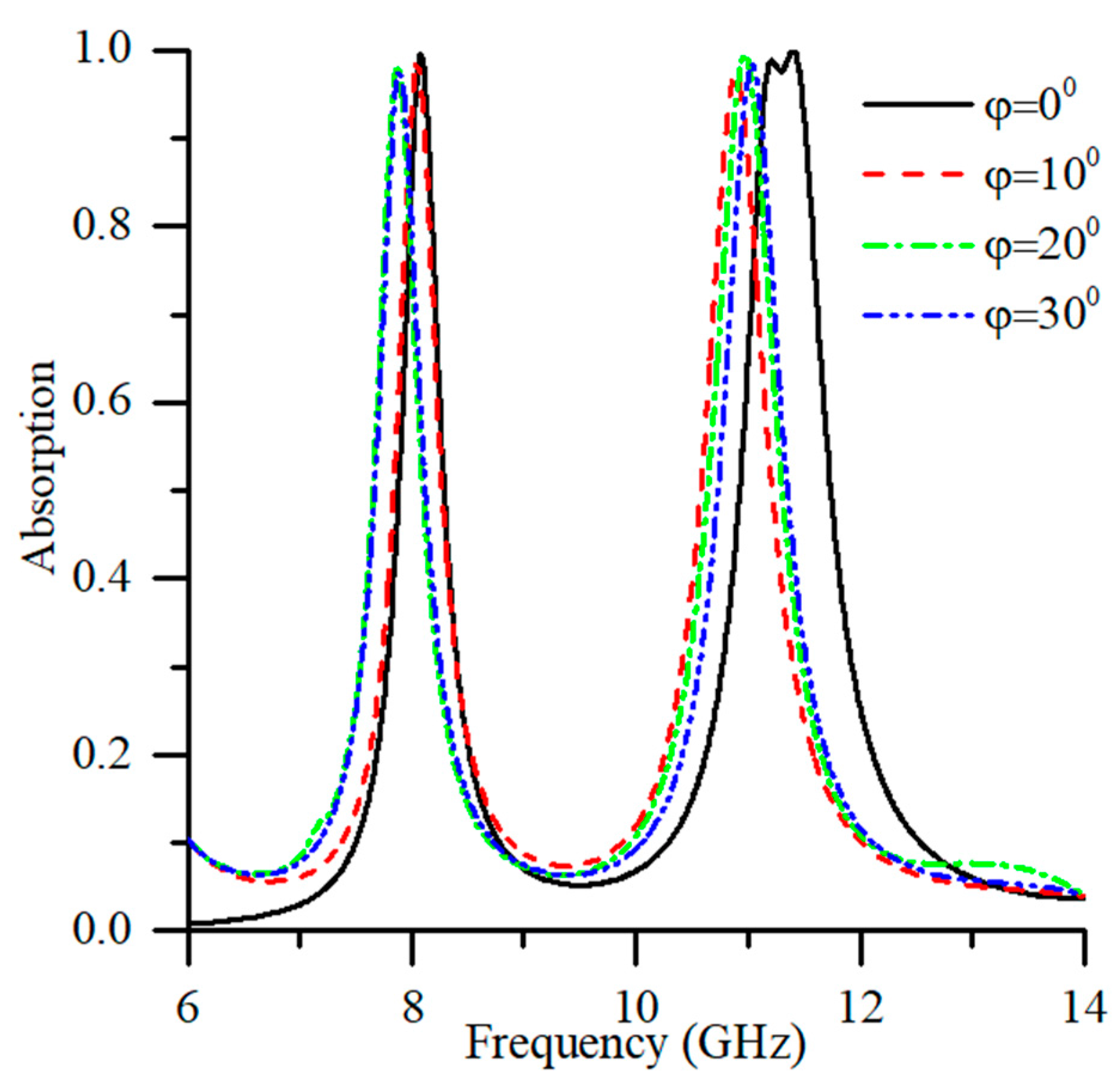
The effect of polarization on the design structure of PMA has been analysed and the results of the absorption is little bit changed for polarization angle. The absorption values for different polarization angle, such as φ = 0°, 10°, 20°, and 30° are demonstrated in Figure 6. It is seen from Figure 6 that the maximum absorption values of design structure are 99.64% at 8.08 GHz, and 99.95% at 11.41 GHz, for 0° polarization; the highest peaks of the absorption are 98.93% at 8.05 GHz, and 97.21% at 10.89 GHz, for 10°; the maximum absorption values of structure are 98.22% at 7.87 GHz, and 99.47% at 10.97 GHz, for 20°; and, the highest peaks of the absorption are 97.54% at 7.89 GHz, and 98.28% at 11.04 GHz, for 30°, respectively. At 0° polarization, the design structure has exhibited highest peak of the absorption. The absorption value is high while the transmittance value is near zero. However, the reflectance value is also less at that point. The polarization of electromagnetic wave has marginally changed the resonance frequencies and absorption values due to altering the material properties.
3.2. Analysis of Design Structure with Different Thickness of FR4 Substrate Materials
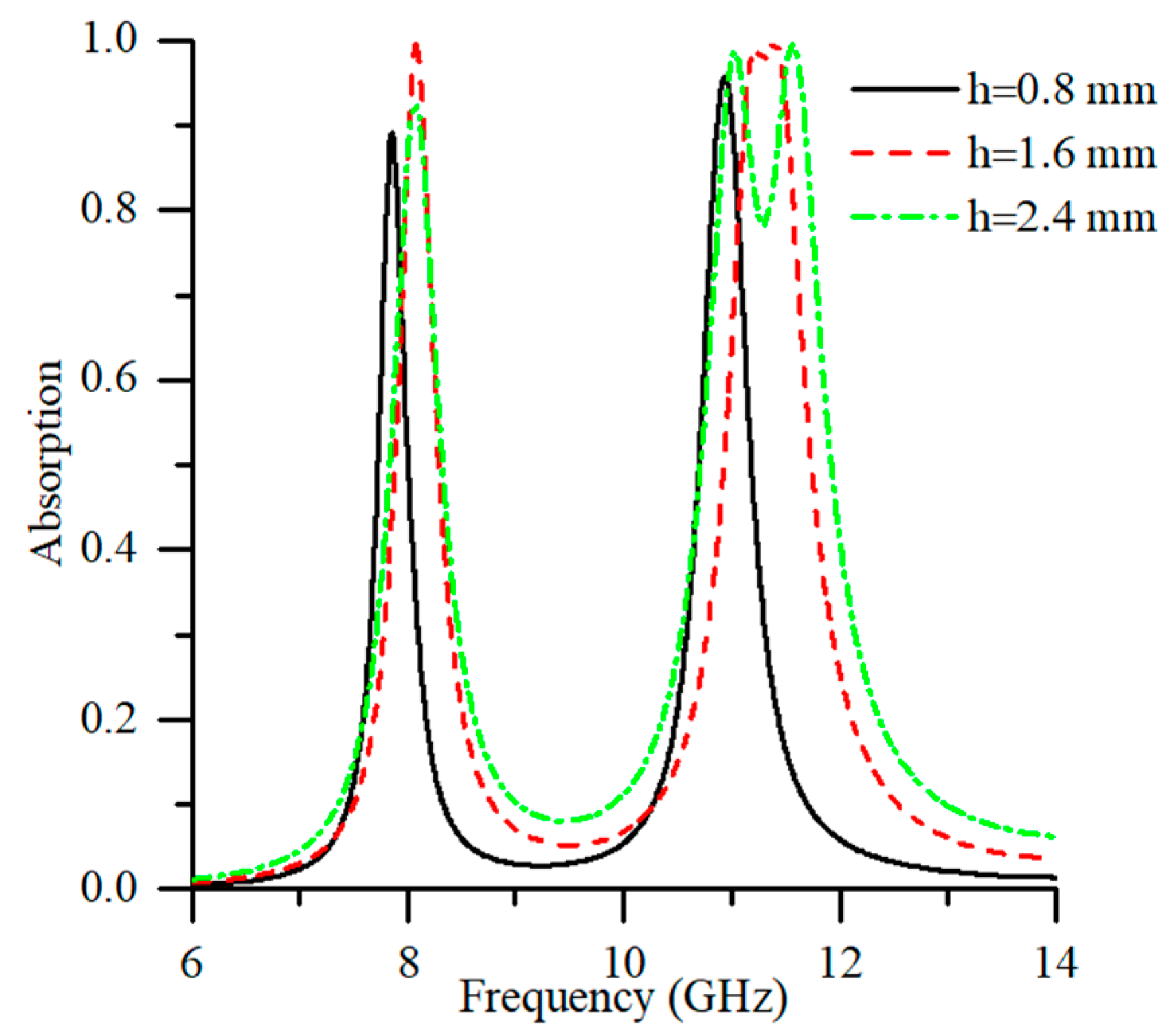
Different thickness of substrate materials, for example, 0.8 mm, 1.6 mm, and 2.4 mm have been considered in the design structure. To observe the absorption, three different thicknesses have been utilized for proposed design. It is observed from Figure 7, the absorption values of the structure are 89.20% at 7.85 GHz, and 95.76% at 10.94 GHz, respectively, for FR4 substrate material with 0.8 mm thick. Similarly, the values of the absorption are 99.64% at 8.08 GHz, and 99.97% at 11.40 GHz, correspondingly for 1.6 mm thickness. Besides, absorption values are 92.88% at 8.07 GHz and 99.56% at 11.57 GHz, individually for 2.4 mm thickness of substrate material. The high absorption value are 99.64% at 8.08 GHz, and 99.97% at 11.40 GHz for 1.6 mm thickness of substrate material. Due to different thickness of substrate material, the absorption rate has been different at different frequencies.
The thickness of substrate material with 1.6 mm has revealed the maximum peak. On the other hand, the minimum peak has been achieved from FR4 substrate material with 2.4 mm thickness.
3.3. Analysis of Design Structure with Different Thickness of Metallic Materials
Thickness of the resonator and ground plane of the PMA has an effect on the absorption of electromagnetic energy. Different thickness like 0.1 mm, 0.2 mm, 0.3 mm, and 0.4 mm have been analyzed in the design structure.
The variation of absorption is shown in Figure 8. The absorption values of the structure are 99.04% at 8.32 GHz and 96.98% at 11.59 GHz, respectively, for metallic material with 0.1 mm thickness. Likewise, the values of the absorption are 97.96% at 8.66 GHz, and 97.39% at 11.89 GHz, correspondingly for 0.2 mm thickness. In addition, absorption values are 96.70% at 9.01 GHz and 99.71% at 12.22 GHz, respectively, for 0.3 mm thickness as well as 99.04% at 9.11 GHz and 99.92% at 12.43 GHz, respectively, for 0.4 mm thickness of copper metallic material. The highest absorption peaks are 99.04% at 9.11 GHz and 99.92% at 12.43 GHz for 0.3 mm thickness of metallic material. Due to different thickness of metallic material, the amount of absorption has been different at different frequencies. The thickness of metallic material with 0.3 mm has shown the maximum peak. However, the minimum peak has been achieved from metallic material with 0.2 mm thick. However, the variation of absorption has occurred in a small amount.
3.4. Analysis of Design Structure with Resistive Load
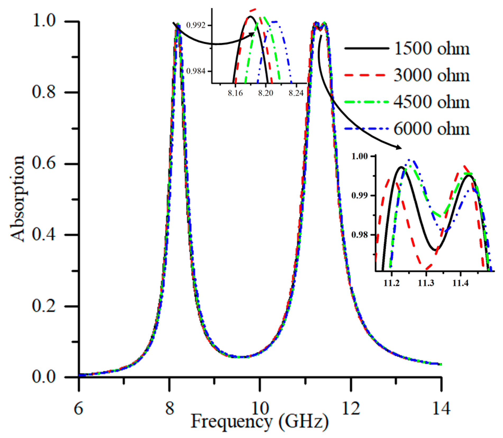
The effects of the resistive load of the octagonal resonators on the absorption have been analysed. The absorption of design structure with different values of a resistive load are shown in Figure 9. The maximum absorption peaks of the structure are 99.40% at 8.17 GHz and 99.74% at 11.23 GHz, respectively, for 1500 Ω resistive load. Similarly, the maximum peak values of the absorption are 99.54% at 8.19 GHz, and 99.77% at 11.41 GHz, correspondingly for 3000 Ω resistive load. Additionally, absorption peak values are 99.41% at 8.20 GHz and 99.76% at 11.26 GHz, respectively, for 4500 Ω resistive load, as well as 99.33% at 8.21 GHz and 99.94% at 11.26 GHz, respectively, for 6000 Ω resistive load that placed between two rings. The high absorption peaks are 99.54% at 8.19 GHz, and 99.77% at 11.41 GHz for 3000 Ω resistive load.
Due to different resistive load, the absorption values have been different at different frequencies. The resistive load with 3000 Ω has shown the maximum absorption value. On the other hand, the minimum value of absorption has been attained from resistive load with 1500 Ω. The effects of resistive load also showed that the performance of absorption of PMA also depends on lumped elements. Furthermore, the absorbing performance has been optimized by proper choice of the lumped resistor of the structure.
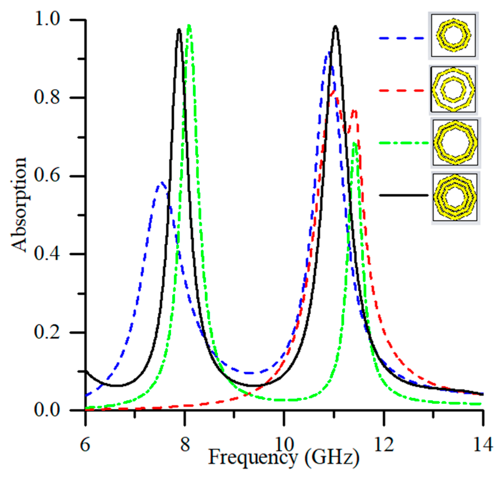
3.5. Analysis of Design Structure with Resonator’s Number
The absorption of electromagnetic energy also is contingent on the resonator’s number used in the structure. Effect of resonator’s number on the substrate material of the PMA has been analyzed. The effect of absorption is shown in Figure 10. The absorption peaks of the structure are 58.35% at 7.54 GHz and 91.97% at 10.89 GHz for two inner resonators. Similarly, the peaks of the absorption are 81.77% at 10.99 GHz for inner and outer resonators. Moreover, absorption peaks are 98.99% at 8.10 GHz and 68.97% at 11.43 GHz, respectively, for two outer resonators. Furthermore, 99.64% at 8.08 GHz and 99.95% at 11.41 GHz, respectively, for three metallic resonators. The maximum absorption peaks are 99.64% at 8.08 GHz and 99.95% at 11.41 GHz, for three metallic resonators.
The absorption values have been different due to the number of metallic resonators. The PMA with three metallic resonators has shown the maximum peak. However, the minimum peak and single absorption peak have been achieved from metallic resonator with the combination of inner and outer resonators. Hence, the variation of absorption has occurred for different ring’s number.
Table 1 demonstrates the comparisons with proposed PMA and another reported PMA. The compared parameters of PMA have been considered here, for example, design structure, size of unit cell structure, applicable band, absorption rate, and year published. Kollatou et al. [21] proposed modified square-shape structure with 8 × 8 mm2 size and obtained absorption of 95.81% in Table 1. Likewise, other authors, Rana et al. in [22], suggested a U-shape absorber for multiband application. On the other hand, authors have achieved 98% absorption with 15 × 15 mm2 size of design structure. Borah et al. [23] exhibited an O-shape with 12 × 12 mm2 dimension of unit cell structure for X-band application. However, Authors obtained absorption of 98.90%. In [17] an S-shape metamaterial absorber was analysed using various substrate materials and different propagation axis of electromagnetic wave. In contrast, authors have obtained a small amount of absorption. Sen et al. recommended L-shape structure with 9 × 9 mm2 dimension for X- and Ku-band operations and attained absorption of 95%. In addition, the authors, Mahmood et al. [24] suggested modified S-shape structure with 16 × 16 mm2 dimensions and achieved absorption of 90%. The compact octagonal shape PMA has been analysed and attained higher absorption (98.97%) with compact size of unit cell (10 × 10 mm2) in this paper. The proposed metamaterial has attained compactness and high absorption comparing mentioned references that are suitable for the microwave regime. In addition, the compact size of the design structure is feasible for X band application. Hence, the manufacturability and robustness of the properties of our design structure are very good for commercial adoption.
4. Conclusions
A new design of compact octagonal shape PMA was proposed for analysing the absorbing properties based on the numerical simulation and experimental results. The geometry of the offered PMA structure was very simple and it showed a high absorption in microwave frequencies. The results of measurement are in agreement with the numerical ones. The suggested PMA is appropriate for x-band microwave application. A comparative analysis also carried out on the basis of the polarization angle of the unit cell, different thickness of substrate and metallic material, number of resonator, and energy absorption with resistive load. The mentioned variation of PMA shows good performance and the values of absorption are around unity. The open-space measurement method was applied to validate the results of the prototype of the structure. The metamaterial structure was compact in size, and high absorption, which makes it ideal for defence and stealth systems.
Acknowledgments
This work was supported by the Ministry of Education (MOE) under Fundamental Research Grant Scheme, Code: FRGS/1/2017/TK04/UKM/02/3.
Author Contributions
Mohammad Jakir Hossain made substantial contributions to the conception, design and analysis. Mohammad Rashed Iqbal Faruque participated in revising the article critically for important intellectual contents. Mohammad Tariqul Islam and Kamarulzaman bin Mat provided necessary instructions for experimental purposes.
Conflicts of Interest
The authors declare no conflict of interest.
References
- Smith, D.R.; Pendry, J.B.; Wiltshire, M.C. Metamaterials and negative refractive index. Science 2004, 305, 788–792. [Google Scholar] [CrossRef] [PubMed]
- Soukoulis, C.M.; Linden, S.; Wegener, M. Negative refractive index at optical wavelengths. Science 2007, 315, 47–49. [Google Scholar] [CrossRef] [PubMed]
- Landy, N.I.; Sajuyigbe, S.; Mock, J.; Smith, D.; Padilla, W. Perfect metamaterial absorber. Phys. Rev. Lett. 2008, 100, 207402. [Google Scholar] [CrossRef] [PubMed]
- Singh, P.; Ameri, S.K.; Chao, L.; Afsar, M.N.; Sonkusale, S. Broadband millimeterwave metamaterial absorber based on embedding of dual resonators. Prog. Electromagn. Res. 2013, 142, 625–638. [Google Scholar] [CrossRef]
- Huang, X.; Yang, H.; Yu, S.; Wang, J.; Li, M.; Ye, Q. Triple-band polarization-insensitive wide-angle ultra-thin planar spiral metamaterial absorber. J. Appl. Phys. 2013, 113, 213516. [Google Scholar] [CrossRef]
- Xu, Y.Q.; Zhou, P.H.; Zhang, H.B.; Chen, L.; Deng, L.J. A wide-angle planar metamaterial absorber based on split ring resonator coupling. J. Appl. Phys. 2011, 110, 044102. [Google Scholar]
- Shrekenhamer, D.; Xu, W.; Venkatesh, S.; Schurig, D.; Sonkusale, S.; Padilla, W.J. Experimental realization of a metamaterial detector focal plane array. Phys. Rev. Lett. 2012, 109, 177401. [Google Scholar] [CrossRef] [PubMed]
- Shrekenhamer, D.; Watts, C.M.; Montoya, J.; Krishna, S.; Padilla, W.J. Metamaterial-based imaging for potential security applications. SPIE OPTO 2013, 8632, 863221. [Google Scholar]
- Xiong, H.; Hong, J.-S.; Luo, C.-M.; Zhong, L.-L. An ultrathin and broadband metamaterial absorber using multi-layer structures. J. Appl. Phys. 2013, 114, 064109. [Google Scholar] [CrossRef]
- Hunt, J.; Driscoll, T.; Mrozack, A.; Lipworth, G.; Reynolds, M.; Brady, D.; Smith, D.R. Metamaterial apertures for computational imaging. Science 2013, 339, 310–313. [Google Scholar] [CrossRef] [PubMed]
- Pfeiffer, C.; Grbic, A. Metamaterial Huygens’ surfaces: Tailoring wave fronts with reflectionless sheets. Phys. Rev. Lett. 2013, 110, 197401. [Google Scholar] [CrossRef] [PubMed]
- Naser-Moghadasi, M.; Nia, A.Z.; Toolabi, M.; Heydari, S. Microwave metamaterial Absorber based on Jerusalem Cross with meandered load for bandwidth enhancement. Opt. Int. J. Light Electron Opt. 2017, 140, 515–522. [Google Scholar] [CrossRef]
- Lin, B.; Zhao, S.; Da, X.; Fang, Y.; Ma, J.; Li, W.; Zhu, Z. Triple-band low frequency ultra-compact metamaterial absorber. J. Appl. Phys. 2015, 117, 184503. [Google Scholar] [CrossRef]
- Zhao, J.; Cheng, Y. Ultrabroadband microwave metamaterial absorber based on electric SRR loaded with lumped resistors. J. Electron. Mater. 2016, 45, 5033–5039. [Google Scholar] [CrossRef]
- Dincer, F.; Karaaslan, M.; Sabah, C. Design and analysis of perfect metamaterial absorber in GHz and THz frequencies. J. Electromagn. Waves Appl. 2015, 29, 2492–2500. [Google Scholar] [CrossRef]
- Hossain, M.J.; Faruque, M.R.I.; Islam, M.T. Design and analysis of a new composite double negative metamaterial for multi-band communication. Curr. Appl. Phys. 2017, 17, 931–939. [Google Scholar] [CrossRef]
- Islam, S.S.; Faruque, M.R.I.; Islam, M.T. Design and absorption analysis of a new multiband split-S-shaped metamaterial. Sci. Eng. Compos. Mater. 2017, 24, 139–148. [Google Scholar] [CrossRef]
- Kim, Y.; Yoo, Y.; Hwang, J.; Lee, Y. Ultra-broadband microwave metamaterial absorber based on resistive sheets. J. Opt. 2016, 19, 015103. [Google Scholar] [CrossRef]
- Wen, Q.-Y.; Zhang, H.-W.; Xie, Y.-S.; Yang, Q.-H.; Liu, Y.-L. Dual band terahertz metamaterial absorber: Design, fabrication, and characterization. Appl. Phys. Lett. 2009, 95, 241111. [Google Scholar] [CrossRef]
- Tao, H.; Bingham, C.; Pilon, D.; Fan, K.; Strikwerda, A.; Shrekenhamer, D.; Padilla, W.J.; Zhang, X.; Averitt, R.D. A dual band terahertz metamaterial absorber. J. Phys. D Appl. Phys. 2010, 43, 225102. [Google Scholar] [CrossRef]
- Kollatou, T.M.; Dimitriadis, A.I.; Assimonis, S.; Kantartzis, N.V.; Antonopoulos, C.S. A family of ultra-thin, polarization-insensitive, multi-band, highly absorbing metamaterial structures. Prog. Electromagn. Res. 2013, 136, 579–594. [Google Scholar] [CrossRef]
- Rana, C.R.; Inamdar, K.; Lalluwadia, A. Study, Design and Analysis of U-Shaped Metamaterial Absorber for X-Band Application. IUP J. Telecommun. 2016, 8, 23. [Google Scholar]
- Borah, D.; Bhattacharyya, N.S. Design and Development of Expanded Graphite-Based Non-metallic and Flexible Metamaterial Absorber for X-band Applications. J. Electron. Mater. 2017, 46, 226–232. [Google Scholar] [CrossRef]
- Mahmood, A.; Yetkin, G.Ö.; Sabah, C. Design and Fabrication of a Novel Wideband DNG Metamaterial with the Absorber Application in Microwave X-Band. Adv. Condens. Matter Phys. 2017, 2017, 1279849. [Google Scholar] [CrossRef]
- Sen, G.; Islam, S.N.; Banerjee, A.; Das, S. Broadband Perfect Metamaterial Absorber on Thin Substrate for X-Band and Ku-Band Applications. Prog. Electromagn. Res. C 2017, 73, 9–16. [Google Scholar] [CrossRef]
Figure 1.
(a) The proposed sketch of perfect metamaterial absorber (PMA); (b) Unit cell with resistive load; (c) The fabricated unit cell structure; (d) Side view of PMA; and, (e) Fabricated array of PMA.
Figure 1.
(a) The proposed sketch of perfect metamaterial absorber (PMA); (b) Unit cell with resistive load; (c) The fabricated unit cell structure; (d) Side view of PMA; and, (e) Fabricated array of PMA.


Figure 2.
(a) The boundary condition of PMA; (b) Measurement set of PMA. PEC: perfect electric conductor; PMC: perfect magnetic conductor; EM: electromagnetic.
Figure 2.
(a) The boundary condition of PMA; (b) Measurement set of PMA. PEC: perfect electric conductor; PMC: perfect magnetic conductor; EM: electromagnetic.
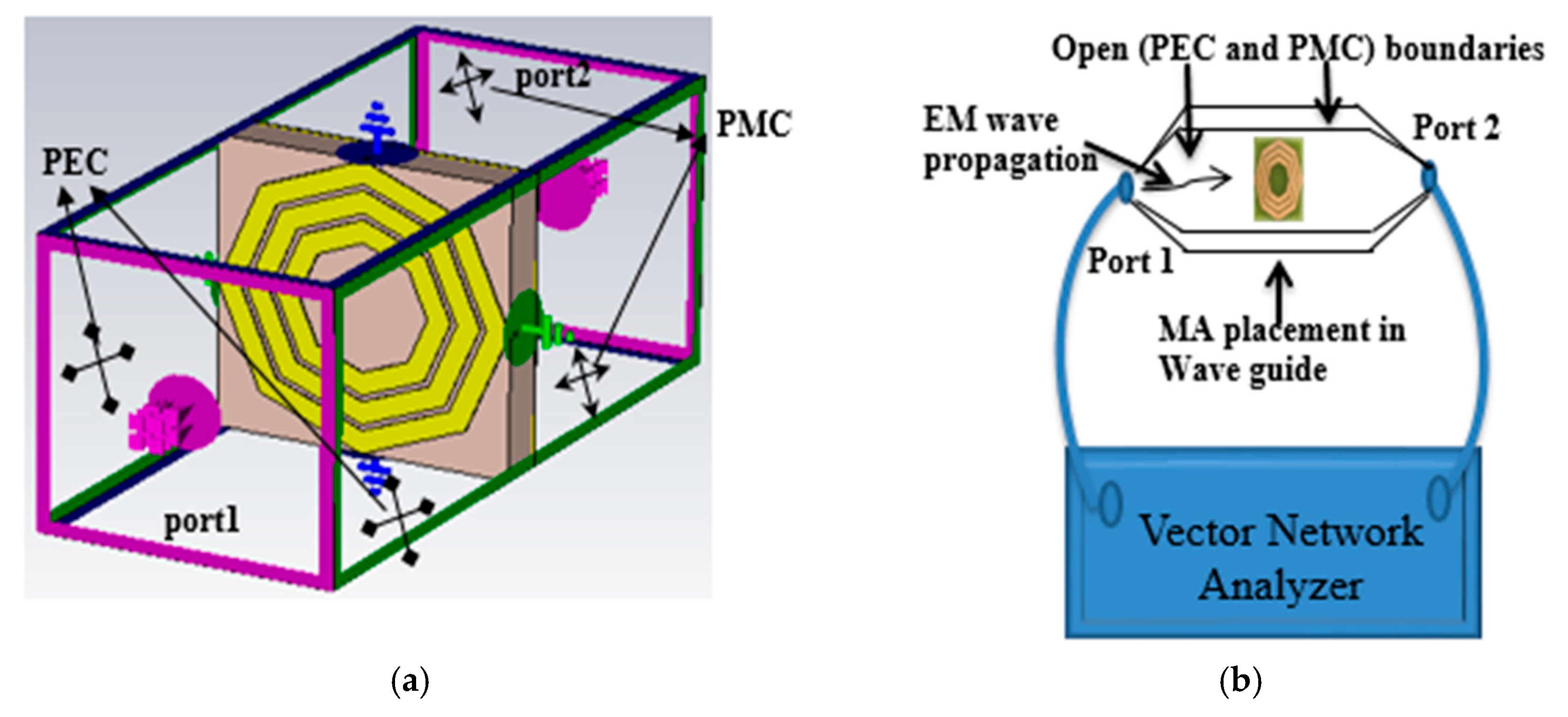
Figure 3.
Simulated-measured of absorption for the proposed PMA.

Figure 4.
(a) Electric field; (b) Magnetic field distribution at resonance frequency 8.08 GHz of PMA.
Figure 4.
(a) Electric field; (b) Magnetic field distribution at resonance frequency 8.08 GHz of PMA.
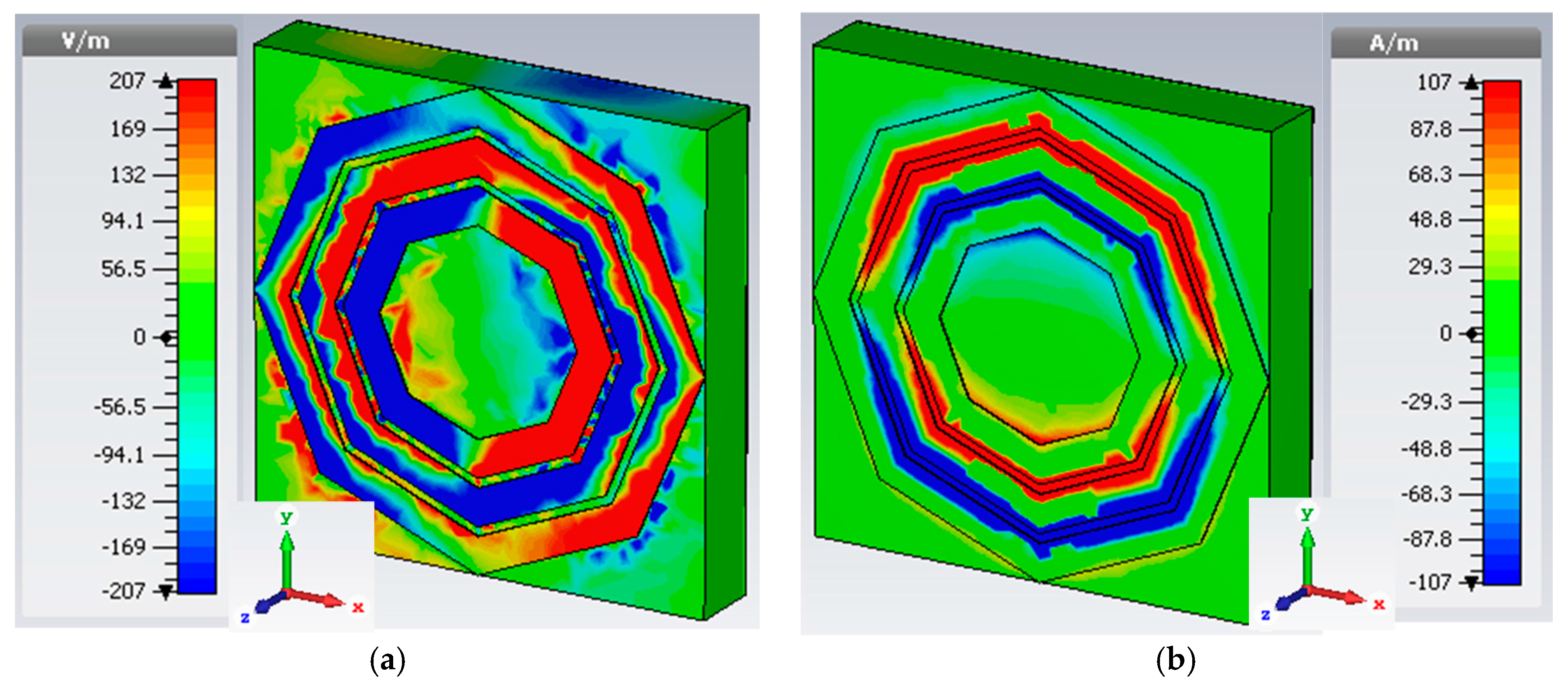
Figure 5.
(a) Electric field; (b) Magnetic field distribution at resonance frequency 11.41 GHz of PMA.
Figure 5.
(a) Electric field; (b) Magnetic field distribution at resonance frequency 11.41 GHz of PMA.
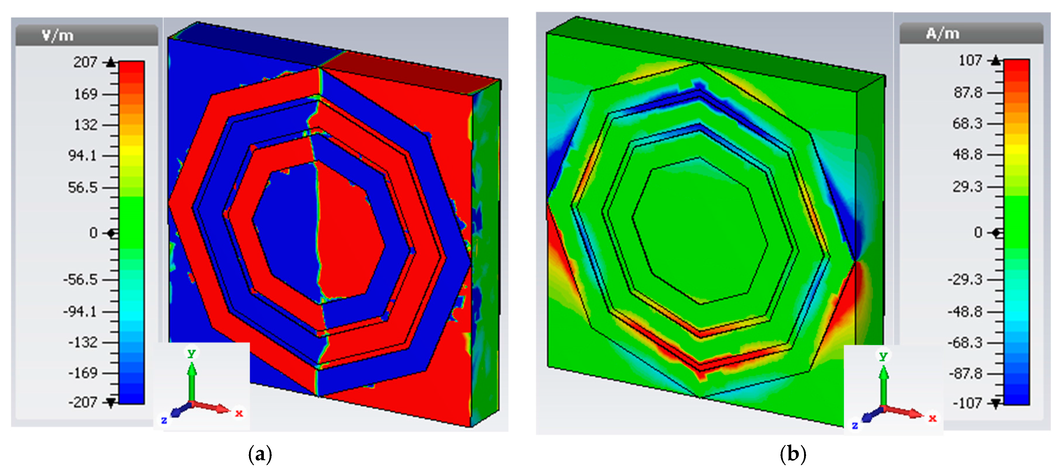
Figure 6.
Absorption of design structure with polarization angle.

Figure 7.
Absorption of the design structure for different thickness of substrate materials.

Figure 8.
Absorption of the design structure for different thickness of metallic materials.
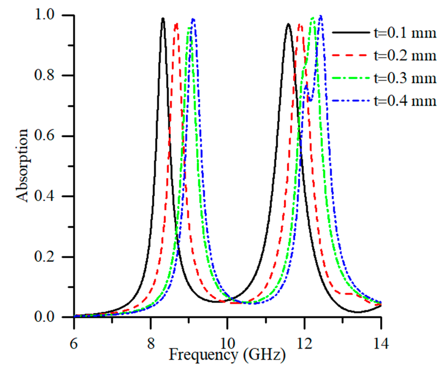
Figure 9.
Absorption of the design structure for different resistive load.

Figure 10.
Absorption of the design structure for number of metallic resonators.

Table 1.
Justification of previous perfect metamaterial absorber (PMA) and proposed PMA.
| Author Name | Design Structure | Size (mm2) | Proposed Band | Absorption Rate (%) | Year of Published |
|---|---|---|---|---|---|
| Kollatou et al. [21] | Modified Square | 8 × 8 | X-band | 95.81 | 2013 |
| Rana et al. [22] | U-shape | 15 × 15 | X-band | 98.00 | 2016 |
| Borah et al. [23] | O-shape | 12 × 12 | X-band | 98.90 | 2016 |
| Islam et al. [17] | S-shape | 20 × 20 | S-, X-, Ku-band | 55.00 | 2017 |
| Sen et al. [25] | L-shape | 9 × 9 | X-, Ku-band | 95.00 | 2017 |
| Mahmood et al. [24] | Modified S-shape | 16 × 16 | X-band | 90.00 | 2017 |
| Proposed PMA | Octagonal shape | 10 × 10 | X-band | 98.97 | - |
© 2017 by the authors. Licensee MDPI, Basel, Switzerland. This article is an open access article distributed under the terms and conditions of the Creative Commons Attribution (CC BY) license (http://creativecommons.org/licenses/by/4.0/).
Share and Cite
MDPI and ACS Style
Hossain, M.J.; Faruque, M.R.I.; Islam, M.T.; Mat, K.B. A New Compact Octagonal Shape Perfect Metamaterial Absorber for Microwave Applications. Appl. Sci. 2017, 7, 1263. https://doi.org/10.3390/app7121263
AMA Style
Hossain MJ, Faruque MRI, Islam MT, Mat KB. A New Compact Octagonal Shape Perfect Metamaterial Absorber for Microwave Applications. Applied Sciences. 2017; 7(12):1263. https://doi.org/10.3390/app7121263
Chicago/Turabian StyleHossain, Mohammad Jakir, Mohammad Rashed Iqbal Faruque, Mohammad Tariqul Islam, and Kamarulzaman Bin Mat. 2017. "A New Compact Octagonal Shape Perfect Metamaterial Absorber for Microwave Applications" Applied Sciences 7, no. 12: 1263. https://doi.org/10.3390/app7121263
Note that from the first issue of 2016, this journal uses article numbers instead of page numbers. See further details here.