Article

Low-Loss Micro-Resonator Filters Fabricated in Silicon by CMOS-Compatible Lithographic Techniques: Design and Characterization

1
Department of Electrical, Computer, and Biomedical Engineering, Università di Pavia, Pavia I-27100, Italy
2
Optoelectronics Research Centre, University of Southampton, Southampton SO17 1BJ, UK
3
Department of Civil Engineering and Architecture, Università di Pavia, Pavia I-27100, Italy
4
Photonic Department, CEA MINATEC Campus, Grenoble CEDEX F-38054, France
5
Istituto Superiore Mario Boella, Torino 10138, Italy
6
Dipartimento di Elettronica e Telecomunicazioni, Politecnico di Torino, Torino 10129, Italy
7
STMicroelectronics-Studio di Microelettronica, Via Ferrata 4, Pavia 27100, Italy
8
Photonic Packaging Group, Tyndall National Institute, Lee Maltings Complex, Cork T12R5CP, Ireland
*
Author to whom correspondence should be addressed.
Appl. Sci. 2017, 7(2), 174; https://doi.org/10.3390/app7020174
Submission received: 10 January 2017 / Revised: 25 January 2017 / Accepted: 7 February 2017 / Published: 11 February 2017
(This article belongs to the Special Issue Silicon Photonics Components and Applications)

Abstract

:
Optical resonators are fundamental building-blocks for the development of Si-photonics-integrated circuits, as tunable on-chip optical filters. In addition to the specific spectral shape, which may vary according to a particular application, extremely low losses from these devices are a crucial requirement. In the current state-of-the-art devices, most low-loss filters have only been demonstrated by exploiting ad hoc lithographic and etching techniques, which are not compatible with the standard CMOS (complementary metal-oxide semiconductor) process-flow available at Si-photonic foundries. In this paper, we describe the design and optimization of optical micro-resonators, based on Si-waveguides with a height lower than the standard ones (i.e., less than 220 nm), prepared on SOI (silicon on insulator) platform, which allow the realization of high-performance optical filters with an insertion loss lower than 1 dB, using only previously validated lithographic etch-depths.

1. Introduction

During the last decade, Silicon (Si) photonics emerged as a promising technology for the integration of optical functionalities within microelectronic chips, with several different components having already been demonstrated [1,2], including optical filters [3,4], modulators [5,6], receivers [7], and wavelength converters [8,9]. The two principal factors motivating Si-photonics are (i) the possibility to realize structures with a very high optical refractive-index contrast; and (ii) the exploitation of Si-processing technologies that have already been developed and validated for the microelectronic device industry, and which have the potential to deliver low cost Si-photonic components, at very high volumes.
Photonic structures with a high index contrast (HIC) allow modal confinement within sub-wavelength dimensions, which allows for reduced waveguide-turning radii, and small component sizes, both of which lead to very small photonic-chip footprints. The realization of high performance HIC structures requires precise designs and accurate fabrication, to ensure that waveguide propagation losses and reflections are sufficiently low. Additionally, as standard telecom single mode fibers have a mode field diameter of the order of 10µm, and HIC waveguides typically have a cross-section of the order of 200 nm × 500 nm, fiber-to-chip coupling is a significant technical challenge, and often introduces a relevant insertion loss (>3 dB [10,11]).
In this article, we focus our attention on the performance of HIC structures for an optical micro-resonator, with ring and racetrack topology, coupled to two separate waveguides. This 4-port configuration allows for the filtering of the selected channel, without affecting the through-signals, and is thus a promising candidate for the realization of optical filters for wavelength division multiplexing (WDM) telecom systems. Thanks to the HIC in the SOI platform, even micro-resonators with a turn-radius of less than 10 µm can be exploited, which brings the advantage of optical filters with a high free-spectral-range (FSR [12,13,14])—a fundamental requirement for application in real systems. The major challenge in realizing these filters is their relatively high optical losses. These losses can be reduced using ad hoc fabrication protocols, such as the steam oxidation and HF-stripping, to reduce waveguide heights, in addition to the standard processes in the Si-Photonic foundry, but this adds cost and complexity to the process [12,15,16]. On the other hand, our target was to implement a carefully designed strategy, so as to obtain the best possible filter performance, whilst only exploiting CMOS-compatible standard processes, as described in Section 2.3.
In this article, we present the results obtained in the frame of the European FP7-project FABULOUS, dedicated to the development of complex integrated optical circuits for innovative high bit-rate passive optical networks (PONs), fabricated by standard-CMOS technologies [17,18]. The final goal, which is the insertion of the chip in a real passive network, imposes very strict requirements on the loss of the component, which has to be kept as low as possible, as the reflective-PON approach yields a very challenging power budget. The filter was designed to meet the aforementioned EU project goals, but its specifications are common to many other potential low-cost WDM optical communication applications; as such, the presented filter design has wide potential applications.
In the following, we first describe the strategy used for the structure’s design, the fabrication technique, and the experimental characterization setup. In the Results Section, we discuss the characterization outcome, which constituted the base for the structure fine-tuning and for the final device fabrication. We then analyze the results obtained in the final fabrication, comparing ring- and racetrack-based devices, as well as with data reported in the literature.

2. Materials and Methods
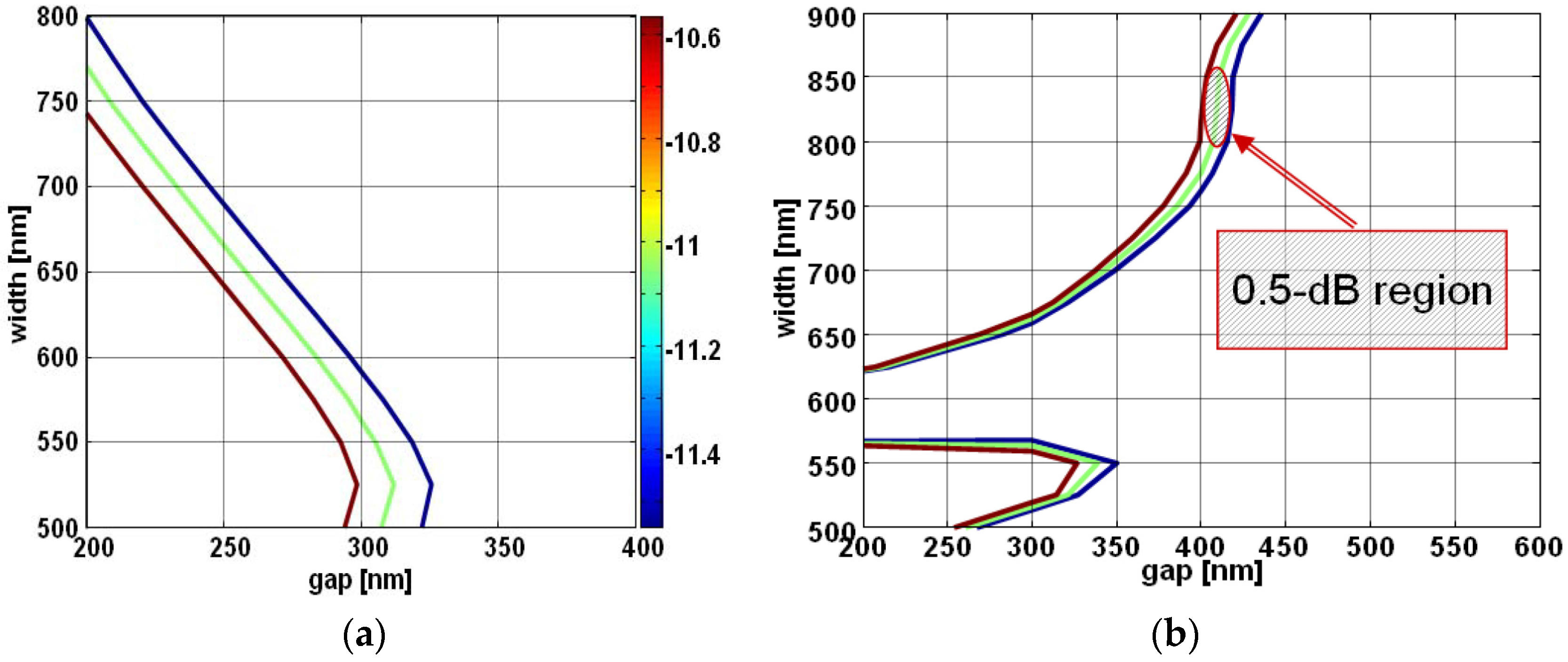
In this section, we first describe the methods used for the filter design, then illustrate the fabrication steps, and finally introduce the characterization setup.

2.1. Filter Design

In order to obtain a proper filter design, we started with a simple mathematical description of an ideal ring resonator transfer function, comparing it with the filter requirements that are reported in Table 1. It is worth noting that the requirements of the adjacent and non-adjacent suppression of channels are relatively relaxed, as the structure of next-generation passive optical network units (ONUs) often has the optical signal passing through two filters. On the other hand, this introduces the requirement of an extremely low filter insertion loss (IL).
By analyzing the filter-cascade transfer function, we determined that a cascade of at least two resonators is required to satisfy the requirements of a Si-photonic-based WDM NG-PON, and that the bus-to-ring (kB) and ring-to-ring (kR) field-coupling-coefficients, should be set to 0.26 and 0.05, respectively.
Following this, we performed a series of 3D-FDTD simulations, to identify the geometry of waveguides and coupling regions that could provide the desired coupling coefficients. All simulations were performed using the commercially available “FDTD Solutions” (by Lumerical Solutions Inc., Vancouver, BC V6E 2M6, Canada), by considering the silicon waveguide and resonator structures to be fully surrounded by SiO2 cladding layers, and by working on TE light polarization. Furthermore, minimum feature sizes and other manufacturing constraints were provided by the fabrication procedures at the CMOS-compatible Si-photonic foundry of CEA-Leti. The principal limits imposed by the fabrication and overall integration requirements are:
  • the minimum gap between adjacent waveguides was set to 200 nm, in order to allow a full-etch of the region using standard lithographic techniques;
  • the bus waveguide had to be 500 nm wide, so as to match the width of the waveguides used for the other components of the final chip;
  • the height of the waveguides could be 220 nm (corresponding to the height of the Si layer present on the SOI wafers), or could be reduced to 100 nm, as a fabrication step with a 120-nm etch depth was already present in the process flow, but no other height-value could be used for the filter’s design;
  • it was important to realize a fabrication-tolerant design, as the fabrication process was based on standard lithographic techniques and was not exploiting the e-beam high-resolution, as often done in scientific research where performance is the main challenge and production-price is not an issue.
Analysis immediately identified that standard (500 × 220 nm, width × height) Si-waveguides could not achieve the required bus-ring coupling coefficient, while maintaining a waveguide-to-waveguide gap > 200 nm. However, by taking advantage of the fact that the TE optical mode propagating in height-reduced waveguides more deeply extends outside of the Si-core (see the top part of Figure 1), it is possible to increase the waveguide coupling coefficients. This creates the possibility of two different solutions, which were investigated separately—(i) the use of race-track resonators with standard waveguide; and (ii) the use of reduced-height waveguides with a curved coupling region.
In both cases, the coupling region is increased, which provides a higher coupling efficiency. In addition, for the second case (curved coupling region), we expect a reduction of propagation losses [19], and a simultaneous increase of the coupling coefficients, as the optical mode further expands outside of the waveguide-core region.
For racetrack-based filters, the length of the straight section was initially determined through numerical simulations, so as to obtain the required coupling (while keeping the gap between the bus waveguide and the resonator equal to 200 nm). The curvature radius was then calculated, based on the free-spectral-range constraints reported in Table 1. Finally, the inter-resonator gap was determined, as once the racetrack shape is fixed, there is only one possible inter-resonator gap which can be used to obtain the desired coupling coefficient kR. The ring-based filters were initially defined so that the ring radius matched the physical length of the racetrack filters, and were then analyzed with regard to the dependence of the coupling coefficients on both the bus-to-ring gap, and the ring-waveguide width. Two principal constraints limited the range of solutions that could be considered—(i) the bus waveguide width was kept equal to 500 nm, to allow easy matching with the other on-chip components; (ii) the waveguide height was set to 100 nm, as this value was achievable without requiring additional processing steps in the fabrication of the overall chip.
It is worth underlining that, while having the possibility to tune the waveguide height would have yielded an interesting degree of freedom, the design efforts were aimed at obtaining the best performance, while using only standard, and previously validated, CMOS processes, available at the CEA-Leti Si-photonics foundry. Therefore, only 220-nm and 100-nm high waveguides were considered.

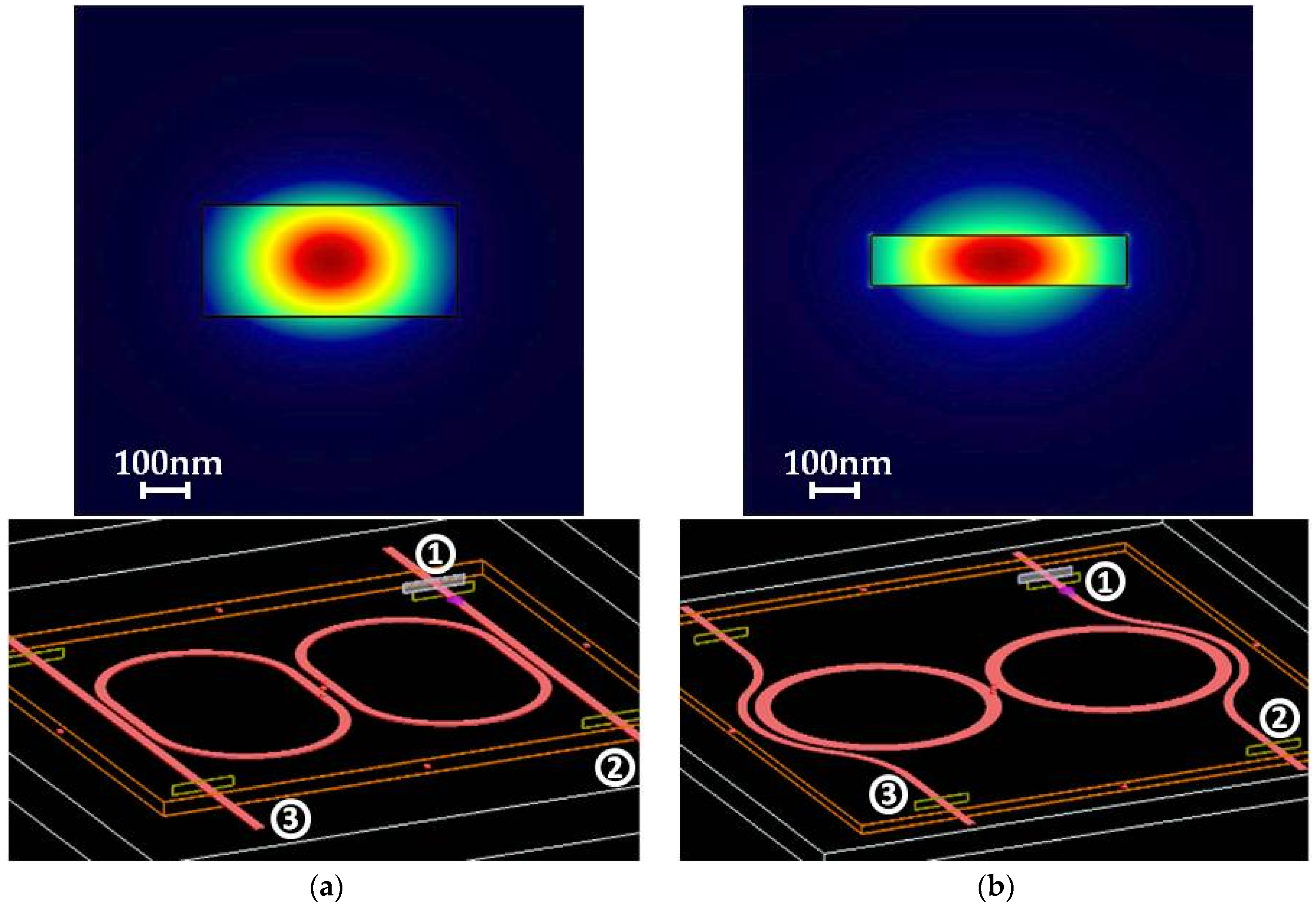
2.2. Structures Parameters

The design procedure for the racetrack-based structure was quite straight-forward, and identified the configuration described in the third column of Table 2.
In contrast, the parameters for the design of the rings-based filters required a deeper analysis, because the necessary coupling coefficient could be obtained by a range of different resonator waveguide-width and Bus-to-Resonator gap combinations. Therefore, the selection of the optimum width-&-gap combinations was made by accounting for the tolerances in the design for minimum feature sizes and fabrication deviations. For this reason, we plotted a contour map of the achievable bus-to-waveguide coupling, expressed in logarithmic units, as a function of the width and gap parameters.
The results of this analysis, shown in Figure 2, highlight that the tolerances offered by different designs can be very different. The plots allow the parameters of the most tolerant design to be identified, for designs with widths in the range of 800–850 nm (i.e., 6% tolerance), and gaps in the range of 400–420 nm (i.e., 5% tolerance). These can still deliver the required coupling coefficient, with a deviation of just ± 0.5 dB. It is worth noticing that, once the waveguide width was selected, the inter-resonator gap can be immediately derived by numerical simulations, because it is the only parameter that can be tuned to achieve the desired kR (see Table 2).

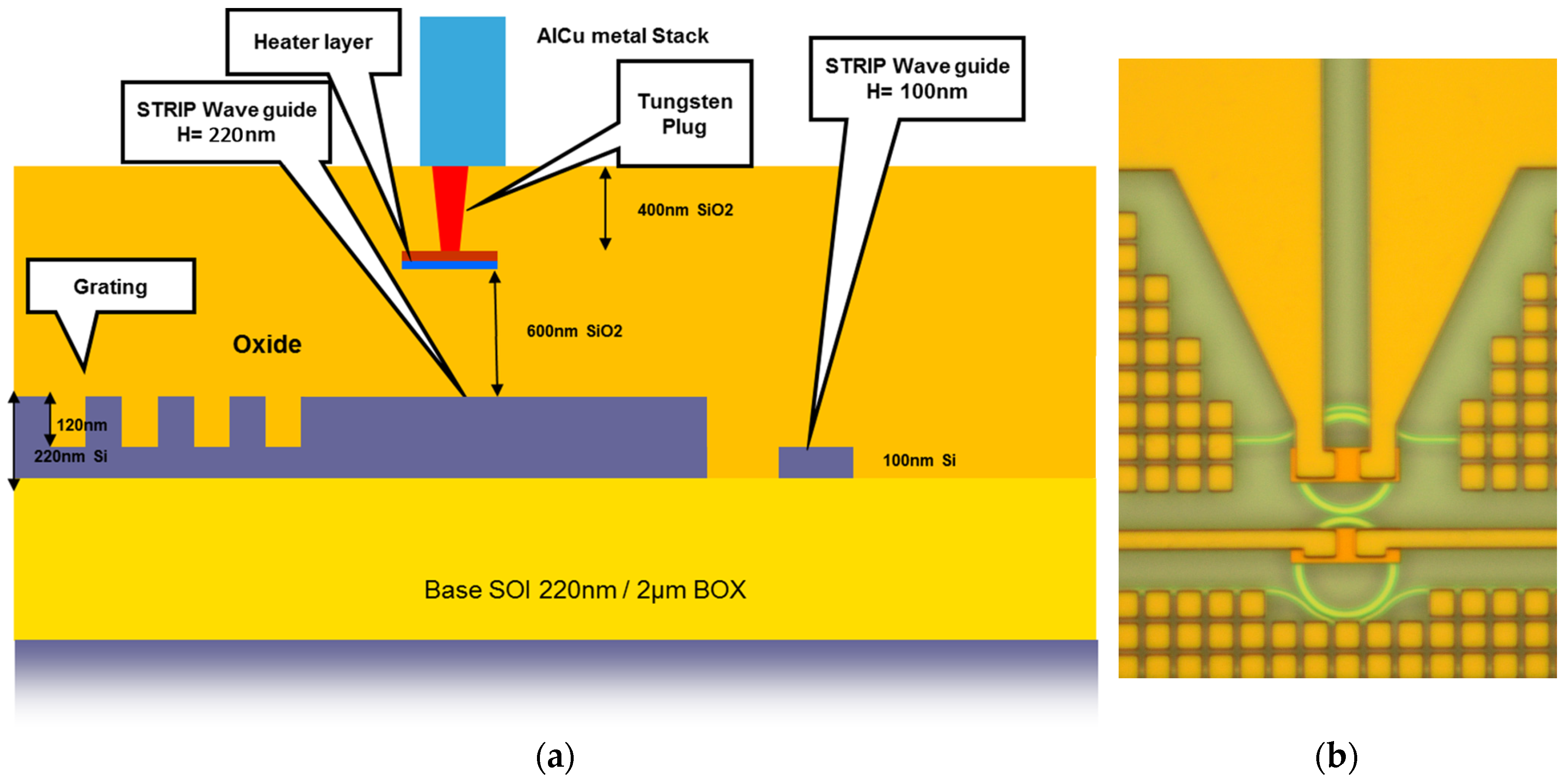
2.3. Fabrication Procedure

The 200 mm SOI (silicon on insulator) wafers have a 220 nm thick silicon-layer, and a 2 µm thick buried oxide layer, and were processed with a MPW (multi-project wafer) run at the CEA-Leti Si-photonics foundry, using standard CMOS process flows. An initial step in the wafer-processing, is the definition of the fiber grating-couplers by 193 nm DUV lithography, and a specific 120 nm partial etch of the Si-layer (with a uniformity better than 3% for the whole wafer). This partial etch is used to pattern the fiber couplers, and to define the height of the reduced-height 100 nm strip waveguides (220 nm Si-layer − 120 nm Si-etch = 100 nm Si-waveguide), used to achieve our low-loss micro-resonator filters. The realized gratings allowed the coupling of light directly from the input fiber to the Si waveguide, which was either 220-nm high or 100-nm high, according to the considered filter design.
The other etching process used has a depth of 220 nm ± 3% (full-etch), and a uniformity of 1.5% for the whole wafer. Both Si-etching processes are performed using ICP RIE, and dry etching equipment is used to obtain very low losses for optical waveguides. It must be noticed that this, fully CMOS-compatible, etching procedure is very different from the strategies that have been exploited in the past in order to realize height-reduced waveguides ([12] and references therein), which required steam oxidation of the Si-layer and subsequent HF stripping.
A HDP (high density plasma) oxide cladding layer encapsulates the waveguide, and optically insulates the waveguide from the Ti/TiN heater, used to tune the filters. The oxide layer thickness is selected to give the best trade-off between heating efficiency and optical losses. The heater consists of a 10nm-thick layer of Ti (used for adhesion), and of a 110 nm-thick TiN resistive layer, that is patterned to create the thermo-optic phase shifter above the waveguide. Finally, a silicon-oxide cladding layer is deposited, and a tungsten via is added, to make contact with the heater layer. This oxide layer provides optical isolations from the aluminum metallization, used for electrical routing to the contact pads. A schematic cross-section of the full device is shown in Figure 3a, with a top-view microscope image of the racetrack-based structure in Figure 3b.

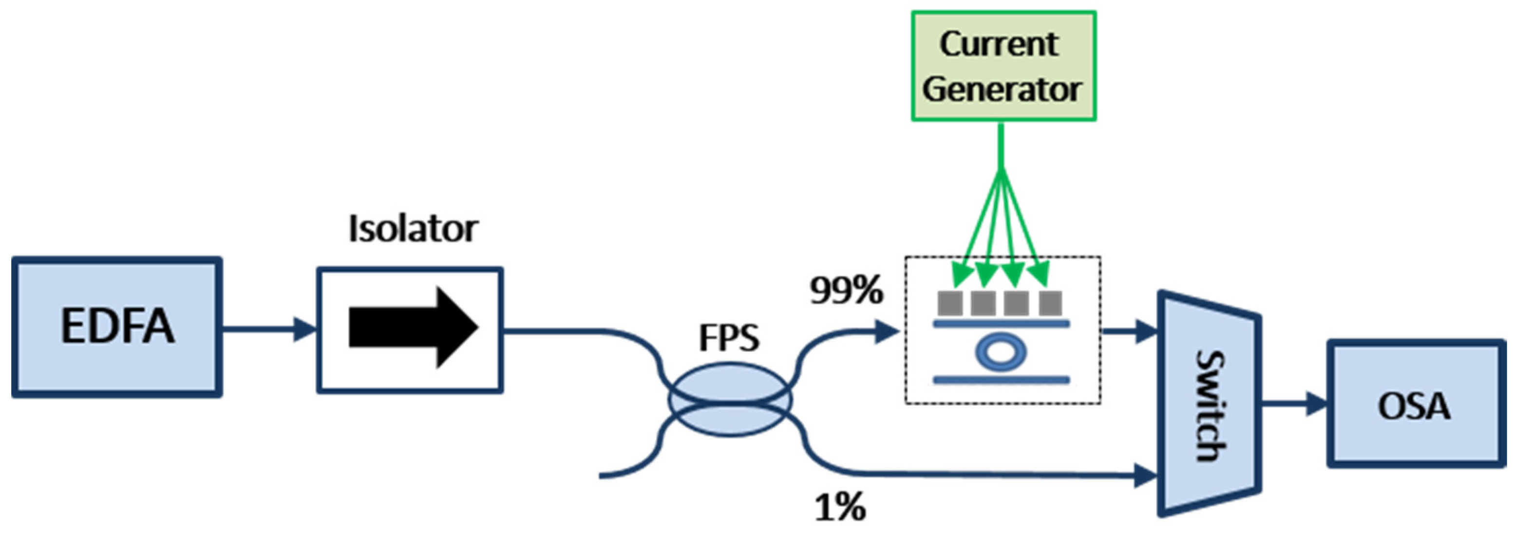
2.4. Experimental Characterization Setup

The experimental set-up used to characterize the filters is shown in Figure 4. The optical input is the broadband ASE (amplified spontaneous emission) from an Erbium-doped fiber amplifier (EDFA). The ASE is first sent to an optical isolator, and then to a 1:99 fiber power splitter—1% of the light is used as a reference to monitor the ASE output, while the remaining 99% is sent to the DUT (device-under-test). 1D-grating couplers are used to couple the light from the ASE fiber-source to/from the Si-PIC with the integrated filters. The output signal from the DUT, together with the 1% monitor signal, are monitored by an optical spectrum analyzer (OSA), using a MEMS-activated optical switch to acquire both spectra. Using stabilized current generators, the resonance wavelengths of the individual rings in the filters can be precisely thermally-tuned.

3. Results

3.1. Experimental Results

The racetrack-based and ring-based filters were experimentally characterized by taking into consideration chips from different parts of the wafer, using the above experimental set-up, with particular attention on evaluating the filter insertion losses and the transfer function spectrum. In Table 3, we report the results of the spectral characterization of the filter exhibiting, for each configuration, the lowest IL.
It is evident from these values that the IL of the filters is still higher than that needed to meet the requirements for practical NG-PONs. In particular, for the rings-based filter, the high losses also result in a significant broadening of the resonance peak, leading to a low suppression of adjacent channels at 100 GHz spacing. In order to improve the performance of the second iterations of these filter designs, we analyze the measured filter performance, to identify possible solutions.

3.2. Final Filter Design

3.2.1. Structures Parameters

Three probable causes for the high losses can be identified (please note that all the experiments were performed using low optical power, so that nonlinear effects can be excluded)—(i) the scattering due to waveguide roughness; (ii) the curvature loss due to waveguide bending; and (iii) the discontinuity of the effective refractive index due to the presence of the coupling region. While the first cause can only be addressed by improving the fabrication processes at the Si-Photonic foundry, the second and third can be mitigated by modifying the filter design.
In our initial design the radius-of-curvature could have been increased, while still satisfying the FSR requirement, but only for the rings-based configuration. This is due to the fact that the effective index in the reduced-height 100-nm waveguides is significantly lower than that in standard 220-nm waveguides, because of the reduced modal confinement in the silicon core. As a consequence, once the optical path length is fixed, the corresponding physical length of resonators based on 100-nm waveguides is longer than that of structures based on 220-nm waveguides. This allows us to increase the ring radius from 6.0 to 8.4 µm, with the expectation of reducing the possible IL-contribution from the waveguide curvature. It is worth mentioning that the biggest contribution to curvature loss is not represented by radiation loss, which is in our case negligible (<0.01 dB/cm even for a ring radius of 6.0 µm), but by the scattering induced because of the interaction of the optical mode, propagating in the bending section with the waveguide lateral-surface roughness.
We can reduce the mode index contrast experienced by light propagating in the coupling region, by increasing the gap between the two waveguides. This is also useful because some areas of the wafer, such as the 200-nm gap, were not fully etched, resulting in a small layer of Si being present between waveguides, which can completely compromise the filter transfer function. In the case of the racetrack configuration, increasing the gap forced an increase in the length of the straight-leg, and a reduction in the radius-of-curvature (to keep the total ring length constant) by approximately 20%, to 3.6 µm. For the modified rings-based configuration, the optimal gap increased by about 25% (from 400 to 515 nm). The final structure parameters of the modified design are reported in Table 4.

3.2.2. Experimental Results

The results collected from the second iteration devices are shown in Table 5; measurements were carried out on replicas of the same optimized filter structures, fabricated on different chips, and the minimum and maximum values obtained at the central resonance (the one closest to 1550 nm) are reported. The experimental results obtained using the newly-designed filter, showed some significant differences and improvements with respect to those of the first iteration in Table 3. In particular, a significant reduction of the insertion loss was observed for the ring-based filter, thanks to the increased radius. An example of the OSA-acquired spectra of the drop and through outputs, for the best performing ring filter, is shown in Figure 5. The performance of the racetrack-based device slightly deteriorated, because of the higher round-trip losses, introduced by the short-radius curves, and because of the change in the modal index between the curved and the straight sections. The variation in the measured absolute resonance wavelength for nominally identical filters, was found to be <0.4 nm for structures fabricated on the same chip, and <4 nm for structures with the same design across different chips.

4. Discussion

Our results demonstrate that, even in a system with strong technological and cost-related constraints, it is possible to reduce filter insertion losses, by carefully optimizing the waveguide cross-section and filter geometry. It is also interesting to note that the choice of a filter design with a relaxed fabrication tolerance, did not reduce filter performances. Comparing our results and designs with those already reported in the literature, this approach seems to be the first time that integrated filters fabricated in Silicon, with insertion losses as low as 0.8 dB, have been obtained (with strip waveguides). With regards to using these filter designs as building blocks for NG-PONs and related fibre-network applications, a comparison of Table 1 and Table 5 shows that the only technical specification which is not satisfied, is the case of the double-ring filter, which has a −3 dB bandwidth in the range 35–39 GHz, instead of being >40 GHz. In any case, due to the high suppression of adjacent channels, this filter is expected to satisfy all requirements, by slightly reducing its bus-to-ring gap.
As nonlinear effects can play a significant role in determining the losses of optical filters, especially for those based on Silicon-resonant cavities, a nonlinear characterization of the integrated filters has been carried out. The target was to estimate the “threshold” input power, which should not be exceeded, in order to avoid a non-linear degradation of the filter performance. For the nonlinear characterization, an external cavity laser (linewidth < 100 kHz), and tunable from 1490 nm to 1590 nm, was used as the optical source, instead of the ASE radiation. The light output from the laser was amplified by an EDFA, and then sent to a fiber polarization controller, in order to maximize the optical power, coupled by the 1D input grating coupler. The rest of the experimental setup is the same as the one presented in Figure 3.
Initially, the laser beam was set at a very low power (<−15 dBm) and its wavelength was tuned to match the filter resonance. The beam power was then progressively increased, while the power output from the drop port of the filter was recorded. The results obtained for the two filter configurations showed a linear relationship between input- and output-power levels (i.e., a constant IL) up to a certain threshold, which depends on the considered filter structure. When the input power is increased above this threshold level, the drop-port output power begins to saturate, due to a number of nonlinear effects, such as two-photon absorption, free-carrier dispersion, and free-carrier absorption. Due to the reduced effective index and lower modal confinement, the reduced height-waveguides have a threshold that is >3 dB higher than that of standard waveguides (500 nm × 220 nm) [20], thus allowing the use of higher power signals in the ONU. In particular, while the threshold power (in the waveguide) for standard waveguides that causes significant nonlinear effects is close to −1 dBm, it is necessary to reach about +4dBm to observe the same effect in the reduced-height structures [19].
As expected, the measured propagation loss of the reduced-height (i.e., 500–800 nm × 100 nm) Si-waveguides is lower than that of standard (i.e., 500 nm × 220 nm) Si-waveguides [19]. While the standard waveguides on the DUT had propagation losses of 2.8–3.0 dB/cm, the propagation losses of the reduced-height waveguides was 2.4–2.7 dB/cm for the 500 nm × 100 nm cross-section, and 1.7–2.0 dB/cm for the 800 nm × 100 nm cross-section.
When comparing our results with [14], which appears to be the only existing publication reporting similar performances, it appears that using rib waveguides has a similar effect to reducing the waveguide height, probably due to the optical mode extending further away from the waveguide axis. The solution reported in [14] allowed an increase in the coupling coefficient of 220-nm height waveguides, and the realization of high performance filters, thanks to the realization of a small bus-ring gap (180-nm, obtained by high resolution lithography). On the other hand, the use of rib waveguides imposes a strong limitation on the minimum curvature radius, and thus on the maximum FSR, which in fact, was limited to about 8 nm. Thanks to our design based on reduced height waveguides, we achieved better performances, both in terms of insertion losses (0.8 dB) and FSR (12.8 nm).

5. Conclusions

This is the first example of a ring-based integrated filter, exploiting SOI-strip waveguides for WDM systems, with an insertion loss as low as 0.8 dB. The result was obtained by a careful analysis of the waveguide dimensions, as well as by a selection of the curved-coupling geometry. Additionally, this result has been achieved using standard CMOS-compatible processes, and can be well suited for the realization of optical ring filters in devices exploiting the current Multi-Project Wafers opportunities.

Acknowledgments

The activity was carried in the frame of the European Project FABULOUS (FDMA Access By Using Low-cost Optical network Units in Silicon photonics). Contract No.: 318704, Specific Targeted Research Project (Call: FP7 ICT 2011-8).

Author Contributions

S.A. and R.G. contributed to define the filter requirements; P.M. and C.L. conceived and designed the devices; V.M. and M.F. were responsible of the device fabrication and process optimization. P.M., C.L. R.M. and I.C. designed the experiments; R.M. and V.V. performed the experiments; R.M., V.V. and C.L. analyzed the data; I.C., E.T., L.C. and G.G. contributed with suggestions and discussions to the data analysis. P.M., I.C. and V.V. wrote the main structure of the paper. All the authors read the paper and contributed with modifications and suggestions.

Conflicts of Interest

The authors declare no conflict of interest. The founding sponsors had no role in the design of the study; in the collection, analyses, or interpretation of data; in the writing of the manuscript, and in the decision to publish the results.

References

  1. Lim, A.E.-J.; Song, J.; Fang, Q.; Li, C.; Tu, X.; Duan, N.; Chen, K.K.; Tern, R.P.-C.; Liow, T.-Y. Review of Silicon Photonics Foundry Efforts. IEEE J. Sel. Top. Quantum Electron. 2014, 20, 405–416. [Google Scholar] [CrossRef]
  2. Thomson, D.; Zilkie, A.; Bowers, J.E.; Komljenovic, T.; Reed, G.T.; Vivien, L.; Marris-Morini, D.; Cassan, E.; Virot, L.; Fédéli, J.-M.; et al. Roadmap on silicon photonics. J. Opt. 2016, 18. [Google Scholar] [CrossRef]
  3. Xia, F.; Rooks, M.; Sekaric, L.; Vlasov, Y. Ultra-compact high order ring resonator filters using submicron silicon photonic wires for on-chip optical interconnects. Opt. Express 2007, 15, 11934–11941. [Google Scholar] [CrossRef] [PubMed]
  4. Bogaerts, W.; De Heyn, P.; Van Vaerenbergh, T.; De Vos, K.; Kumar Selvaraja, S.; Claes, T.; Dumon, P.; Bienstman, P.; Van Thourhout, D.; Baets, R. Silicon microring resonators. Laser Photonics Rev. 2012, 6, 47–73. [Google Scholar] [CrossRef]
  5. Reed, G.T.; Mashanovich, G.; Gardes, F.Y.; Thomson, D.J. Silicon optical modulators. Nat. Photonics 2010, 4, 518–526. [Google Scholar] [CrossRef] [Green Version]
  6. Thomson, D.J.; Gardes, F.Y.; Fedeli, J.M.; Zlatanovic, S.; Hu, Y.; Kuo, B.P.P.; Myslivets, E.; Alic, N.; Radic, S.; Mashanovich, G.Z.; et al. 50-Gb/s silicon optical modulator. IEEE Photonics Technol. Lett. 2012, 24, 234–236. [Google Scholar] [CrossRef]
  7. Fang, Q.; Liow, T.Y.; Song, J.F.; Ang, K.W.; Yu, M.B.; Lo, G.Q.; Kwong, D.L. WDM multi-channel silicon photonic receiver with 320 Gbps data transmission capability. Opt. Express 2010, 18, 5106–5113. [Google Scholar] [CrossRef] [PubMed]
  8. Espinola, R.L.; Dadap, J.I.; Richard, M.; McNab, S.J.; Vlasov, Y.A. C-band wavelength conversion in silicon photonic wire waveguides. Opt. Express 2005, 13, 4341–4349. [Google Scholar] [CrossRef] [PubMed]
  9. Yamada, K.; Fukuda, H.; Tsuchizawa, T.; Watanabe, T.; Shoji, T.; Itabashi, S. All-optical efficient wavelength conversion using silicon photonic wire waveguide. IEEE Photonics Technol. Lett. 2006, 18, 1046–1048. [Google Scholar] [CrossRef]
  10. Roelkens, G.; Vermeulen, D.; Van Thourhout, D.; Baets, R.; Brision, S.; Lyan, P.; Gautier, P.; Fédéli, J.M. High efficiency diffractive grating couplers for interfacing a single mode optical fiber with a nanophotonic silicon-on-insulator waveguide circuit. Appl. Phys. Lett. 2008, 92, 131101. [Google Scholar] [CrossRef]
  11. Taillaert, D.; Van Laere, F.; Ayre, M.; Bogaerts, W.; Van Thourhout, D.; Bienstman, P.; Baets, R. Grating couplers for coupling between optical fibers and nanophotonic waveguides. Jpn. J. Appl. Phys. 2006, 45, 6071–6077. [Google Scholar] [CrossRef]
  12. Dahlem, M.S.; Holzwarth, C.W.; Khilo, A.; Kärtner, F.X.; Smith, H.I.; Ippen, E.P. Reconfigurable multi-channel second-order silicon microring-resonator filterbanks for on-chip WDM systems. Opt. Express 2011, 19, 306–316. [Google Scholar] [CrossRef] [PubMed]
  13. Nawrocka, M.S.; Liu, T.; Wang, X.; Panepucci, R.R. Tunable silicon microring resonator with wide free spectral range. Appl. Phys. Lett. 2006, 89, 71110. [Google Scholar] [CrossRef]
  14. Hu, T.; Wang, W.; Qiu, C.; Yu, P.; Qiu, H.; Zhao, Y.; Jiang, X.; Yang, J. Thermally tunable filters based on third-order microring resonators for WDM applications. IEEE Photonics Technol. Lett. 2012, 24, 524–526. [Google Scholar] [CrossRef]
  15. Luo, L.W.; Wiederhecker, G.S.; Cardenas, J.; Poitras, C.; Lipson, M. High quality factor etchless silicon photonic ring resonators. Opt. Express 2011, 19, 6284–6289. [Google Scholar] [CrossRef] [PubMed]
  16. Xiao, S.; Khan, M.H.; Shen, H.; Qi, M. Compact silicon microring resonators with ultra-low propagation loss in the C band. Opt. Express 2007, 15, 14467–14475. [Google Scholar] [CrossRef] [PubMed]
  17. Abrate, S.; Straullu, S.; Nespola, A.; Savio, P.; Chang, J.; Ferrero, V.; Charbonnier, B.; Gaudino, R. Overview of the FABULOUS EU Project: Final System Performance Assessment with Discrete Components. J. Lightwave Technol. 2016, 34, 798–804. [Google Scholar] [CrossRef]
  18. Straullu, S.; Savio, P.; Chang, J.; Ferrero, V.; Nespola, A.; Gaudino, R.; Abrate, S. Optimization of Reflective FDMA-PON Architecture to Achieve 32 Gb/s Per Upstream Wavelength Over 31 dB ODN Loss. J. Lightwave Technol. 2015, 33, 474–480. [Google Scholar] [CrossRef]
  19. Barwicz, T.; Haus, H.A. Three-dimensional analysis of scattering losses due to sidewall roughness in microphotonic waveguides. J. Lightwave Technol. 2005, 23, 2719–2732. [Google Scholar] [CrossRef]
  20. Lacava, C.; Marchetti, R.; Vitali, V.; Cristiani, I.; Giuliani, G.; Fournier, M.; Bernabe, S.; Minzioni, P. Reduced nonlinearities in 100-nm high SOI waveguides. In Proceedings of the SPIE Photonic West 2016, Optical Interconnects XVI, San Francisco, CA, USA, 13–18 February 2016; Schröder, H., Chen, R.T., Eds.; SPIE International: Bellingham, WA, USA, 2016; Volume 9753, pp. 975313–975318. [Google Scholar]
Figure 1. Schemes of the considered waveguides (1 × 1 µm area) and structures: ports 1, 2, and 3 are the input, through, and drop ports, respectively. (a) Top: cross-section of the 500 × 220 nm waveguide and optical TE mode power-distribution. Bottom: 3D figure of the racetrack-resonators; (b) Top: cross-section of the 500 × 100 nm waveguide and optical TE mode power-distribution, showing a lighter-blue area outside the waveguide with respect to the left panel. Bottom: 3D figure of the ring-resonators showing the curved-coupling region.
Applsci 07 00174 g001
Figure 2. The green line shows the combination yielding the desired coupling coefficient. The red and blue lines correspond to an over and under coupling of 0.5 dB, respectively. (a) Contour map obtained considering a straight-coupling geometry; (b) Contour map obtained for curved-coupling geometry.
Applsci 07 00174 g002
Figure 3. (a) Section view of the chip; (b) Microscope-image of the double-ring filter with tuning electrodes.
Applsci 07 00174 g003
Figure 4. Experimental set-up. EDFA: erbium doped fiber amplifier; FPS: fiber power splitter; OSA: optical spectrum analyzer. The continuous lines represent the fiber optic connections.
Applsci 07 00174 g004
Figure 5. OSA-acquired spectra from the drop and through output channel of the best performing ring filter, showing an insertion loss of 0.8 dB. The insertion loss due to grating-coupling is about 7 dB/grating, and the ripple present on the green line is due to a grating-to-grating parasitic cavity.
Applsci 07 00174 g005
Table 1. Desired filter characteristics.
ParameterValue
Operation band1530–1570 nm
Channel spacing100 GHz
Free Spectral Range12.8 nm
Insertion Loss<1 dB
Suppression adjacent channels>15 dB
Suppression non-adjacent channels>20 dB
Table 2. Parameters used for the first fabrication of the filters.
ParameterUnitsRacetracksRings
Bus waveguide (width × height)nm × nm500 × 220500 × 100
Resonator waveguide (width × height)nm × nm500 × 220825 × 100
Straight-legnm4745N.A.
Curve radius (@ waveguide center)nm44906000
Bus-to-Resonator gapnm200410
Inter-Resonator gapnm415340
Table 3. Best values measured on filters based on the first design.
ParameterUnitsRacetracksRings
Insertion LossdB2.04.6
−3 dB BandwidthGHz4773
−20 dB BandwidthGHz158208
Suppression @ 100 GHzdB2419
Table 4. Parameters used for the second fabrication of the filters.
ParameterUnitsRacetracksRings
Bus waveguide (width × height)nm × nm500 × 220500 × 100
Resonator waveguide (width × height)nm × nm500 × 220800 × 100
Straight-legnm8160N.A.
Curve radius (@ waveguide center)nm36008400
Bus-to-Resonator gapnm250515
Inter-Resonator gapnm460355
Table 5. Minimum and maximum values measured on filters based on the second design.
ParameterUnitsRacetracksRings
Insertion LossdB1.9–2.90.8–1.5
−3 dB BandwidthGHz37–4035–39
−20 dB BandwidthGHz115–13195–109
Suppression @ 100 GHzdB26–3530–35
Thermo-optical tuning efficiency mW/nm2.5–2.64.8–5.5

