Article

Electronically Tunable Current Controlled Current Conveyor Transconductance Amplifier-Based Mixed-Mode Biquadratic Filter with Resistorless and Grounded Capacitors

1
Department of Electronic Engineering, Ming Chi University of Technology, New Taipei 24301, Taiwan
2
Department of Computer and Communication Engineering, De Lin Institute of Technology, New Taipei 23654, Taiwan
*
Author to whom correspondence should be addressed.
Appl. Sci. 2017, 7(3), 244; https://doi.org/10.3390/app7030244
Submission received: 22 December 2016 / Revised: 27 February 2017 / Accepted: 1 March 2017 / Published: 4 March 2017

Abstract

:
A new electronically tunable mixed-mode biquadratic filter with three current controlled current conveyor transconductance amplifiers (CCCCTAs) and two grounded capacitors is proposed. With current input, the filter can realise lowpass (LP), bandpass (BP), highpass (HP), bandstop (BS) and allpass (AP) responses in current mode and LP, BP and HP responses in transimpedance mode. With voltage input, the filter can realise LP, BP, HP, BS and AP responses in voltage and transadmittance modes. Other attractive features of the mixed-mode biquadratic filter are (1) the use of two grounded capacitors, which is ideal for integrated circuit implementation; (2) orthogonal control of the quality factor (Q) and resonance angular frequency (ωo) for easy electronic tenability; (3) low input impedance and high output impedance for current signals; (4) high input impedance for voltage signal; (5) avoidance of need for component-matching conditions; (6) resistorless and electronically tunable structure; (7) low active and passive sensitivities; and (8) independent control of the voltage transfer gains without affecting the parameters ωo and Q.

1. Introduction

Current-mode active elements have attracted the attention of analogue circuit designers because of their advantages over conventional operational amplifiers, which include higher accuracy, wider frequency response, larger dynamic range, greater linearity, lower power consumption and simpler implementation [1,2]. Thus, applications and advantages of various active filter transfer functions that use different active elements have been studied intensively [3,4,5,6,7,8,9,10,11,12]. Depending on the nature of input and output signals, filters are classified as current-mode (CM), voltage-mode (VM), transadmittance-mode (TAM) and transimpedance-mode (TIM) filters. In a VM structure, both input and output signals are voltages while in a CM structure, both input and output signals are currents. The TAM and TIM structures can function as bridges for transferring VM to CM and vice versa. Hence, mixed-mode circuits are worthy of study. Many types of mixed-mode circuits have been developed [13,14,15,16,17,18,19,20,21,22,23,24,25,26,27], utilizing assorted types of active elements such as conventional second-generation current conveyors (CCIIs) [13,14], current feedback operational amplifiers (CFOAs) [15], differential voltage current conveyors (DVCCs) [16], differential difference current conveyors (DDCCs) [17], fully differential current conveyors (FDCCIIs) [18], four-terminal floating nullors (FTFNs) [19], operational transconductance amplifiers (OTAs) [20,21,22], current controlled current conveyors (CCCIIs) [23,24,25], and current controlled current conveyor transconductance amplifiers (CCCCTAs) [26,27]. High performance electronically tunable active components have also received much attention. In CCCII and OTA, X-port parasitic resistance RX and transconductance gain gm, that are electronically controllable by the input bias currents IS and IB, respectively, have become the most promising active elements in the field of analogue circuit design. Thus, several electronically tunable mixed-mode biquadratic filters have been presented in the literature [20,21,22,23,24,25]. In the literature, circuits with different filter responses are realised according to the selected input signals, and they usually require two/three voltage signals for realising bandstop/allpass (BS/AP) filters and hence other active elements are needed to duplicate the input voltage signals. An attractive feature of multifunction active biquadratic filters is that lowpass (LP), bandpass (BP) and highpass (HP) outputs are simultaneously available in various circuit modes. These additional outputs can be used in systems that employ more than one filter function. Circuits that simultaneously use LP, BP and HP filters have applications in crossover networks used in three-way high-fidelity loudspeakers, touch-tone telephone systems and phase-locked loop frequency modulation stereo demodulators [12]. Simultaneously obtaining various filter functions in the same circuit topology increases the flexibility and versatility of practical applications.
Although several electronically tunable mixed-mode multifunction biquads with multiple-output current controlled conveyors (MOCCCIIs) and two grounded capacitors have been proposed [23,24,25], these circuits [24,25] suffer from the high-input impedance terminal in both VM and TAM. One interesting solution is the electronically tunable mixed-mode circuit [26]. Three CCCCTAs and two grounded capacitors were used to realise LP, BP and HP responses in all four modes in the same configuration. Both BS and AP responses can be realised in CM and TAM, but the AP response in CM and TAM requires a component-matching condition. Another valuable electronically tunable mixed-mode universal biquadratic filter structure with three CCCCTAs and two grounded capacitors was proposed in [27]. The circuit joins one more important advantage of orthogonal controllability of the resonance angular frequency (ωo) and quality factor (Q) and enables implementation of all standard filtering functions in CM and TAM, but a component-matching condition is still needed to realise the AP response in TAM.
This study proposes a new configuration for realising electronically tunable mixed-mode universal biquadratic filters. The proposed circuit employs three CCCCTAs and two grounded capacitors. When operating in CM/TAM, the circuit can simultaneously realise LP, BP and HP filtering responses. The BS/AP filtering responses are also obtained with interconnection of the relevant output currents without any component-matching conditions. When operating in TIM, the circuit can simultaneously realise LP, HP and two BP filtering responses. The LP, BP, HP and BS/AP filtering responses are also obtained simultaneously in VM operation. The advantages of the proposed circuit are the following: (1) resistorless and electronically tunable structure; (2) simultaneous realisation of three generic filtering responses in all the four possible modes; (3) capability to realise BS and AP filtering responses in the VM, CM and TAM without critical component-matching conditions; (4) low-input and high-output impedances for current signals; (5) high-input impedance for voltage signal; (6) use of only grounded capacitors; (7) orthogonal control of the parameters Q and ωo of the filter; (8) independent control of the VM filter gains without affecting the parameters Q and ωo; and (9) low active and passive sensitivity performances. Table 1 and Table 2 compare the proposed circuit with previously reported mixed-mode biquad circuits. It is interesting to note that the proposed circuit only employs three multiple-output CCCCTA active components and two grounded capacitors. Regarding the CCCCTA-based biquads proposed in [26,27], the proposed circuit does not require component-matching conditions to realise the AP response in CM and TAM, and two more standard filter signals can be obtained in VM. Another attractive feature is the independent tunability of the VM filter transfer gain constants without affecting the parameters ωo and Q. Moreover, the CM filter enjoys a low-input and high-output impedance feature, which is a desirable feature for the CM cascading. Since the proposed circuit does not require external resistors and uses only grounded capacitors, it is suitable for integrated circuit (IC) implementation. Table 3 and Table 4 compare the main features of the proposed circuit with those of previous CCCCTA-based works [26,27].

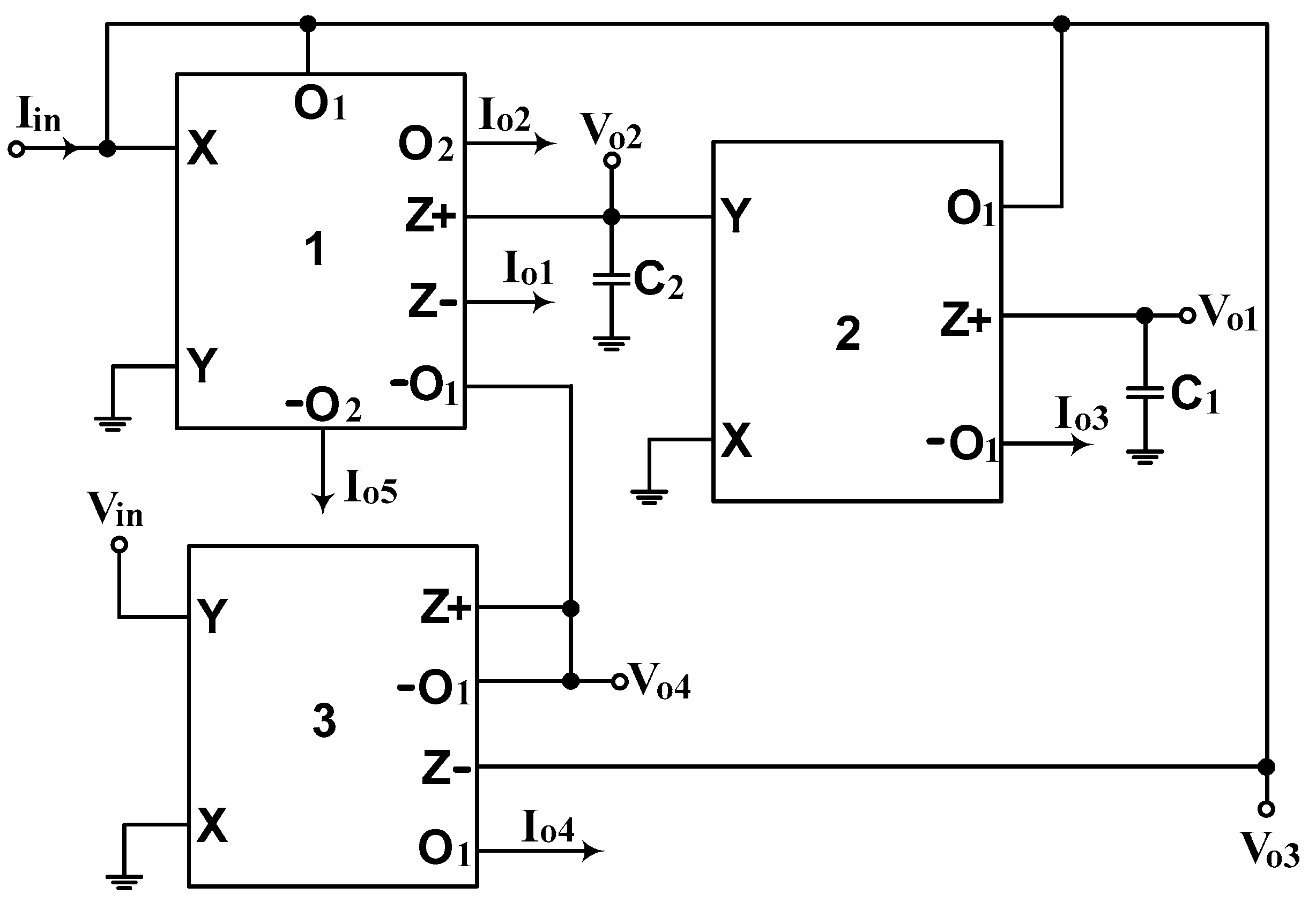
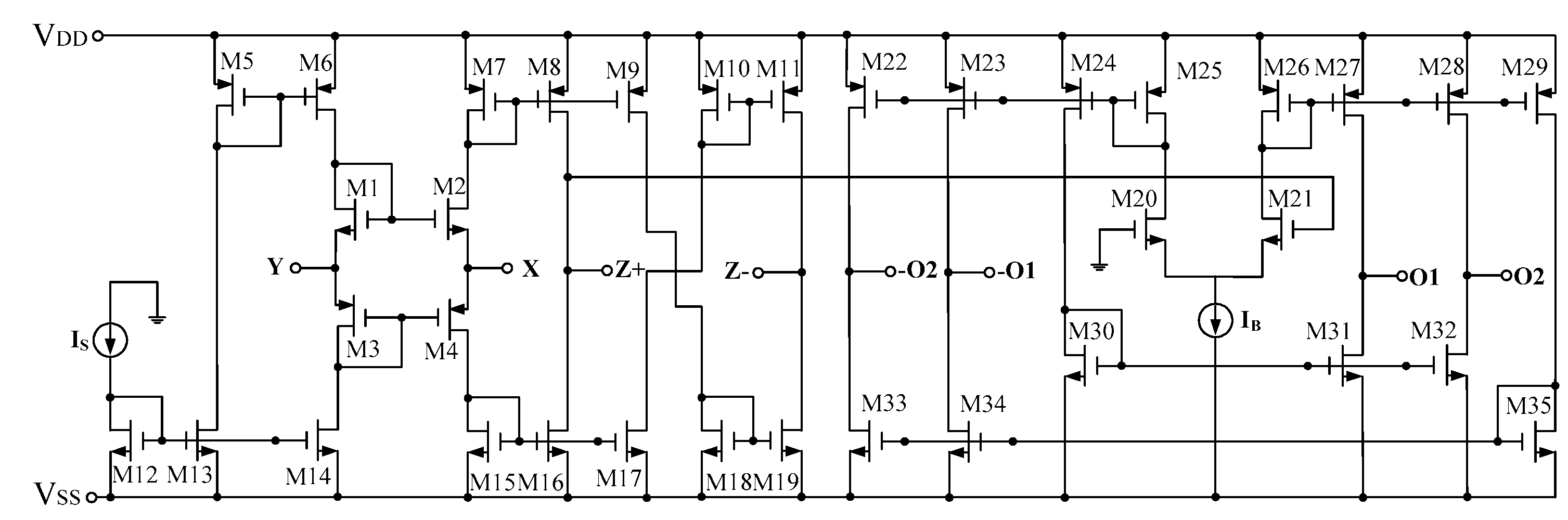
2. Circuit Descriptions

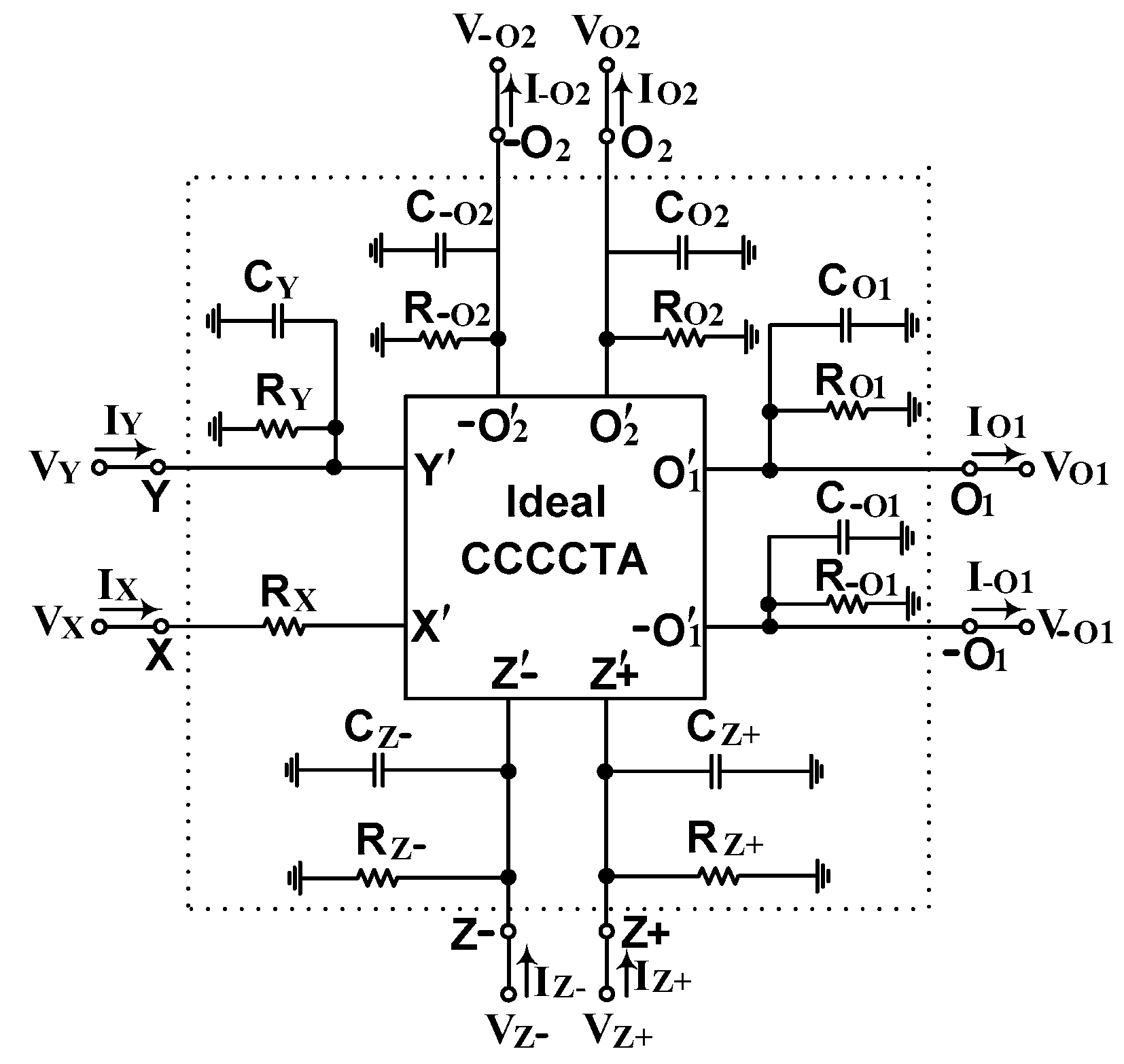
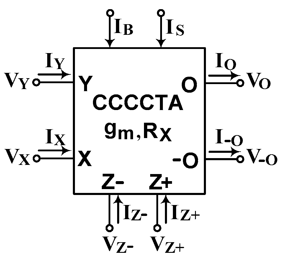
2.1. Basic Concept and Implementation of the CCCCTA

The CCCCTA simplifies circuit implementation by providing an active building block. The CCCCTA device is obtained by cascading the CCCII with the OTA to implement analogue function circuits in compact monolithic chips [28,29]. This versatile component also has potential applications in analogue signal-processing circuits. Because its parasitic resistance and transconductance can be adjusted electronically by the input bias currents IS and IB, respectively, it does not require a resistor in practical applications, which is an attractive feature for filter designers. Figure 1 shows the circuit symbol of the CCCCTA [29]. The port relations of CCCCTA can be characterized by the following matrix equation [26,27,28,29]:
[ I Y V X I Z + I Z I O I O ] = [ 0 0 0 0 0 0 R X 1 0 0 0 0 1 0 0 0 0 0 1 0 0 0 0 0 0 0 g m 0 0 0 0 0 g m 0 0 0 ] [ I X V Y V Z + V Z V O V O ]
where Rx and gm are the parasitic resistance at X-terminal and the transconductance gain of the CCCCTA, respectively. The parasitic resistance Rx can be controlled by the bias current IS of CCCCTA, and the transconductance gain gm can be controlled by the bias current IB of CCCCTA.

2.2. Proposed Electronically-Tunable Mixed-Mode Biquadratic Filter

Figure 2 shows that the proposed electronically tunable mixed-mode biquadratic filter employs three CCCCTAs and two grounded capacitors. The multiple current outputs of the CCCCTA are easily implemented by adding output branches to the CCCCTA. The input current of the circuit is applied to the X-terminal of the first CCCCTA, which has low input impedance. The output currents are obtained at high output impedance ports, which simplifies cascading in both CM and TAM operations. The input voltage of the circuit is applied to the Y-terminal of the third CCCCTA, which has high input impedance. Because the circuit has low input impedance and high output impedance for current signals and has high input impedance for voltage signal, it can be used in cascade for realizing higher-order filters [16]. Moreover, grounded capacitors are used in integrated circuits to cancel parasitic impedance effects of active elements [16]. Routine analysis of the circuit in Figure 2 reveals that the following four output voltages and five output currents can be obtained.
V o 1 = G X 1 G X 2 ( I in G X 3 V in ) D ( s )
V o 2 = sC 1 G X 1 ( I in G X 3 V in ) D ( s )
V o 3 = s 2 C 1 C 2 ( I in G X 3 V in ) D ( s )
V o 4 = ( 1 g m 3 ) sC 1 g m 1 G X 1 I in + G X 3 ( s 2 C 1 C 2 G X 1 + g m 2 G X 1 G X 2 ) V in D ( s )
I o 1 = s 2 C 1 C 2 G X 1 ( I in G X 3 V in ) D ( s )
I o 2 = sC 1 g m 1 G X 1 ( I in G X 3 V in ) D ( s )
I o 3 = g m 2 G X 1 G X 2 ( I in G X 3 V in ) D ( s )
I o 4 = sC 1 g m 1 G X 1 I in + G X 3 ( s 2 C 1 C 2 G X 1 + g m 2 G X 1 G X 2 ) V in D ( s )
I o 5 = sC 1 g m 1 G X 1 ( I in G X 3 V in ) D ( s )
D(s) is given by
D ( s ) = s 2 C 1 C 2 G X 1 + sC 1 g m 1 G X 1 + g m 2 G X 1 G X 2
where G X 1 = 1 R X 1 , G X 2 = 1 R X 2 , and G X 3 = 1 R X 3 .

2.2.1. CM and TIM

According to Equations (2)–(10), CM and TIM can be obtained by setting the input voltage Vin = 0 (grounded) and getting Iin as input signal. The five current transfer functions obtained are:
I o 1 I in = s 2 C 1 C 2 G X 1 D ( s )
I o 2 I in = sC 1 g m 1 G X 1 D ( s )
I o 3 I in = g m 2 G X 1 G X 2 D ( s )
I o 4 I in = I o 5 I in = sC 1 g m 1 G X 1 D ( s )
Equations (12)–(15) indicate that a non-inverting HP filtering response is obtained from Io1, an inverting BP filtering response is obtained from Io2, a non-inverting LP filtering response is obtained from Io3, and two non-inverting BP filtering responses are obtained from Io4 and Io5. The BS filtering response is easily obtained by adding the two currents Io1 and Io3 to obtain the following transfer function:
I BS I in = I o 1 + I o 3 I in = s 2 C 1 C 2 G X 1 + g m 2 G X 1 G X 2 D ( s )
Similarly, the AP transfer function is easily obtained by adding the three currents Io1, Io2 and Io3 to obtain the following transfer function:
I AP I in = I o 1 + I o 2 + I o 3 I in = s 2 C 1 C 2 G X 1 sC 1 g m 1 G X 1 + g m 2 G X 1 G X 2 D ( s )
Thus, all five standard filtering responses are provided by the same CM biquadratic filter structure, and no other component-matching conditions are needed. Notably, all current outputs are available from high-output impedance terminals. High-output impedance terminals of the configuration enable the circuit to be cascaded without additional current buffers. Because the gain of the current-mode HP, LP and BP filters is unity, the additional current amplifiers are needed if a variable gain of current-mode filter is necessary. In addition, the BS and AP filters cannot be realised simultaneously with the HP, LP and BP filters. This problem can be solved by adding the multiple current outputs that can be easily implemented by simply adding output branches.
According to Equation (11), filter parameters ωo and Q are:
ω o = g m 2 G X 2 C 1 C 2 ,   Q = 1 g m 1 g m 2 G X 2 C 2 C 1
Based on Equation (18), parameter Q can be independently tuned by using gm1 without disturbing ωo. Restated, parameters ωo and Q are orthogonally adjustable through the finite input conductance GX2 and then the gm1 in that order. This property is desirable in biquadratic filters because it increases design and tuning flexibility.
Accordingly, the four TIM transfer functions in this case can be obtained as follows:
V o 1 I in = G X 1 G X 2 D ( s )
V o 2 I in = sC 1 G X 1 D ( s )
V o 3 I in = s 2 C 1 C 2 D ( s )
V o 4 I in = ( 1 g m 3 ) sC 1 g m 1 G X 1 D ( s )
As indicated by Equations (19)–(22), an inverting LP filtering response is obtained from Vo1, an inverting BP filtering response is obtained from Vo2, a non-inverting HP filtering response is obtained from Vo3, and a non-inverting BP filtering response is obtained from Vo4. That is, the circuit provides TIM HP, LP and two BP responses simultaneously without disturbing circuit topology.

2.2.2. VM and TAM

According to Equations (2)–(10), VM and TAM can be obtained by setting the input voltage Iin = 0 (opened) and getting Vin as input signal. The four voltage transfer functions obtained are:
V o 1 V in = G X 1 G X 2 G X 3 D ( s )
V o 2 V in = sC 1 G X 1 G X 3 D ( s )
V o 3 V in = s 2 C 1 C 2 G X 3 D ( s )
V o 4 V in = ( G X 3 g m 3 ) ( s 2 C 1 C 2 G X 1 + g m 2 G X 1 G X 2 D ( s ) )
As indicated by Equations (23)–(26), a non-inverting LP filtering response is obtained from Vo1, a non-inverting BP filtering response is obtained from Vo2, an inverting HP filtering response is obtained from Vo3, and a non-inverting BS filtering response is obtained from Vo4. Notably, connecting the output current signal Io5 to the output voltage node Vo4 also obtains a non-inverting AP transfer function in VM as follows:
V o 4 V in = ( G X 3 g m 3 ) ( s 2 C 1 C 2 G X 1 sC 1 g m 1 G X 1 + g m 2 G X 1 G X 2 D ( s ) )
The gain constants in Equations (23)–(26) are
H o 1 = G X 3 g m 2 ,   H o 2 = G X 3 g m 1 ,   H o 3 = G X 3 G X 1 ,   H o 4 = G X 3 g m 3
In Equation (18), the proposed filter orthogonally controls ωo and Q by tuning conductance GX2 for ωo and then tuning transconductance gain gm1 for Q without disturbing parameter ωo. According to Equation (28), the VM filter transfer gains can be independently controlled by changing GX3 without affecting ωo and Q, and the finite input conductance GX3 at the X-terminal of the CCCCTA(3) is tunable. Therefore, the VM filter provides orthogonal tunability of all three filter parameters (ωo, Q and Ho) in all five responses. This is because the three output voltages Vo1, Vo2 and Vo4 are not in low-output impedance terminals. Voltage followers are needed for the proposed circuit to drive low impedance loads or to be directly connected to the next stages.
Accordingly, the five TAM transfer functions in this case are obtained as follows:
I o 1 V in = s 2 C 1 C 2 G X 1 G X 3 D ( s )
I o 2 V in = sC 1 g m 1 G X 1 G X 3 D ( s )
I o 3 V in = g m 2 G X 1 G X 2 G X 3 D ( s )
I o 4 V in = s 2 C 1 C 2 G X 1 G X 3 + g m 2 G X 1 G X 2 G X 3 D ( s )
I o 5 V in = sC 1 g m 1 G X 1 G X 3 D ( s )
As indicated by Equations (29)–(33), an inverting HP filtering response is obtained from Io1, a non-inverting BP filtering response is obtained from Io2, an inverting LP filtering response is obtained from Io3, a non-inverting BS filtering response is obtained from Io4 and an inverting BP filtering response is obtained from Io5. Thus, the proposed filter can simultaneously realise LP, BP, HP and BS responses in TAM. The TAM AP transfer function is easily obtained by adding currents Io4 and Io5, which yields the following transfer function:
I AP V in = I o 4 + I o 5 V in = s 2 C 1 C 2 G X 1 G X 3 sC 1 g m 1 G X 1 G X 3 + g m 2 G X 1 G X 2 G X 3 D ( s )
Table 5 summarizes the four possible modes of the transfer functions according to Equations (2)–(10).

2.3. Non-Ideal Analysis and Sensitivity Performance

If the non-idealities of CCCCTA are considered, the relationships of the terminal voltages and currents can be rewritten as V X = β V Y + I X R X , I Z + = α p I X , I Z = α n I X , I O 1 = γ p g m V Z + , I O 1 = γ n g m V Z + , I O 2 = η p g m V Z + and I O 2 = η n g m V Z + , where β, αp, αn, γp, γn, ηp and ηn are CCCCTA transfer ratios that deviate from unity by the transfer errors [27]. In a non-ideal case with reanalysis of the proposed circuit in Figure 2, the denominator of the non-ideal voltage transfer function is yielded as follows:
D ( s ) = β 1 s 2 C 1 C 2 G X 1 + α p 1 β 1 γ p 1 sC 1 g m 1 G X 1 + α p 1 α p 2 β 1 β 2 γ p 2 g m 2 G X 1 G X 2
where βi, αpi and γpi are the parameters β, αp and γp, respectively, of the ith CCCCTA (i = 1, 2, 3).
The non-ideal expressions for ωo and Q are obtained as follows:
ω o = α p 1 α p 2 β 2 γ p 2 g m 2 G X 2 C 1 C 2 ,   Q = 1 γ p 1 g m 1 α p 2 β 2 γ p 2 g m 2 G X 2 C 2 α p 1 C 1
The active and passive sensitivities of the proposed circuit are
S α p 1 ω o = S α p 2 ω o = S β 2 ω o = S γ p 2 ω o = S g m 2 ω o = S G X 2 ω o = S C 1 ω o = S C 2 ω o = 1 2
S α p 2 Q = S β 2 Q = S γ p 2 Q = S g m 2 Q = S G X 2 Q = S C 2 Q = S α p 1 Q = S C 1 Q = 1 2
S γ p 1 Q = S g m 1 Q = 1
These calculation results indicate that all sensitivities are low and have absolute values no larger than unity. The proposed circuit thus exhibited low sensitivity.

2.4. Effect of the CCCCTA Parasitic Impedances and Design Considerations

Next, various parasitic impedances of the CCCCTA in the proposed circuit were studied. Figure 3 represents the non-ideal CCCCTA model including its parasitic elements. A port Y parasitic is in the form RYi//CYi, a port Z+ parasitic is in the form RZi+//CZi+, a port Z− parasitic is in the form RZi−//CZi−, a port O1 parasitic is in the form RO1i//CO1i, a port O2 parasitic is in the form RO2i//CO2i, a port –O1 parasitic is in the form R–O1i//C–O1i, a port –O2 parasitic is in the form R–O2i//C–O2i, and a port X parasitic is in the form RXi where i = 1, 2, 3 and indicates the ith CCCCTA. After applying the non-ideal equivalent circuit mode of the CCCCTA in the proposed circuit, the denominator of the transfer functions becomes:
D ( s ) = m R 3 p s 2 + n 2 g m 1 s + n 1 n 2 g m 2
where,
n 1 = ( 1 R X 2 ) sR 1 p 1 + sR 1 p C 1 = ( 1 R X 2 C 1 ) ( s s + ω 1 ) ,   ω 1 = 1 R 1 p C 1
n 2 = ( 1 R X 1 ) sR 2 p 1 + sR 2 p C 2 = ( 1 R X 1 C 2 ) ( s s + ω 2 ) ,   ω 2 = 1 R 2 p C 2
m = 1 + sR 3 p C 3 p = 1 ω 3 ( s + ω 3 ) ,   ω 3 = 1 1 R 3 p C 3 p
C 1 = C 1 / / C Z 2 + , C 2 = C 2 / / C Z 1 + / / C Y 2 , C 3 P = C O 11 / / C O 12 / / C Z 3 - , R 1 p = R Z 2 + , R 2 p = R Z 1 + / / R Y 2 , and R 3 p = R X 1 / / R O 11 / / R O 12 / / R Z 3 - .
Equations (41)–(43) illustrate that the effects of parasitic elements depend on three parasitic poles yielded by the non-idealities of CCCCTAs. For near-ideal frequency operation, the operating frequency must be higher than ω1 and ω2 and lower than ω3. Therefore, the useful frequency range of the proposed filter is limited by the following conditions:
10 × max { ω 1 , ω 2 } < < ω < < 0.1 ω 3
This condition is easily satisfied since the external capacitance can be set much higher than the parasitic capacitance. In Figure 2, the effects of CCCCTA parasitic elements on the proposed filter can be ignored under the following conditions: min (C1, C2) >> parasitic capacitances (CZ1+, CZ2+, CY2), parasitic resistances (RO11, RO12, RZ3−) >> RX1, 1/sC1 << RZ2+ and 1/sC2 << RZ1+//RY2.
According to (44), the effects of parasitic elements on coefficients n1, n2 and m diminish under the conditions | s | > > ω 1 , | s | > >   ω 2 and | s | < < ω 3 . Hence,
n 1 1 R X 2 C 1
n 2 1 R X 1 C 2
m 1
By substituting Equations (45)–(47) into Equation (40) and assuming that (RO11, RO12, RZ3−) >> RX1, the characteristic equation is:
D ( s ) = s 2 C 1 C 2 G X 1 + sC 1 g m 1 G X 1 + g m 2 G X 1 G X 2
In this case, ωo and Q become:
ω o = G X 2 g m 2 C 1 C 2 ,   Q = 1 g m 1 G X 2 g m 2 C 2 C 1
Thus, the effects of CCCCTA parasitic elements on the proposed filter in Figure 2 can be ignored in this case.

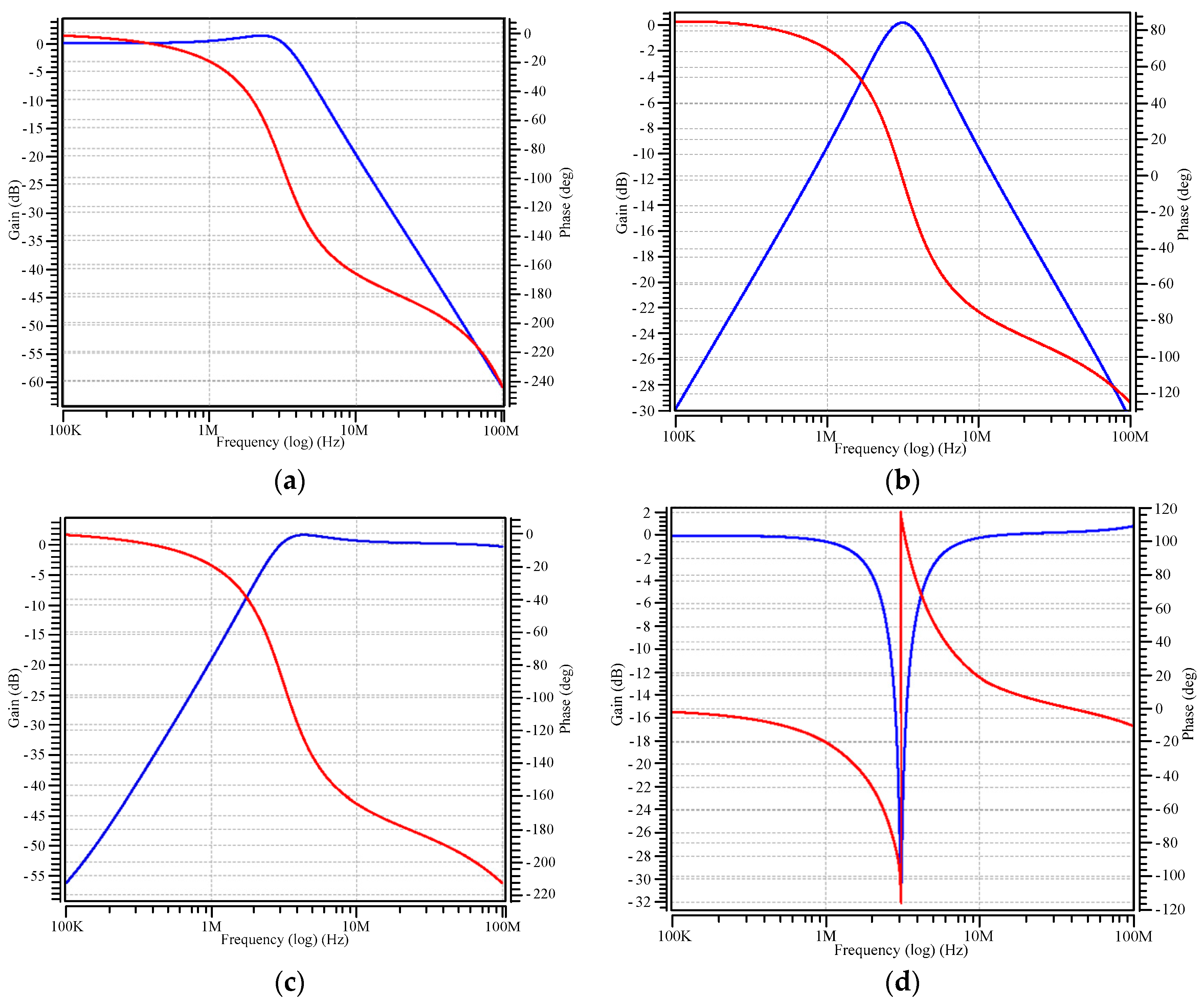
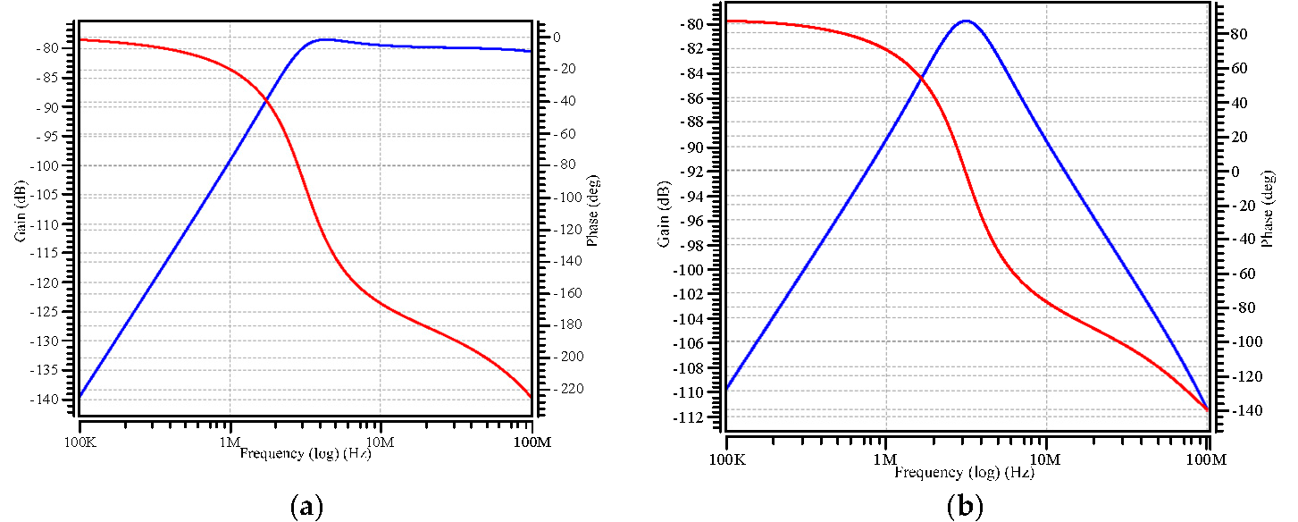
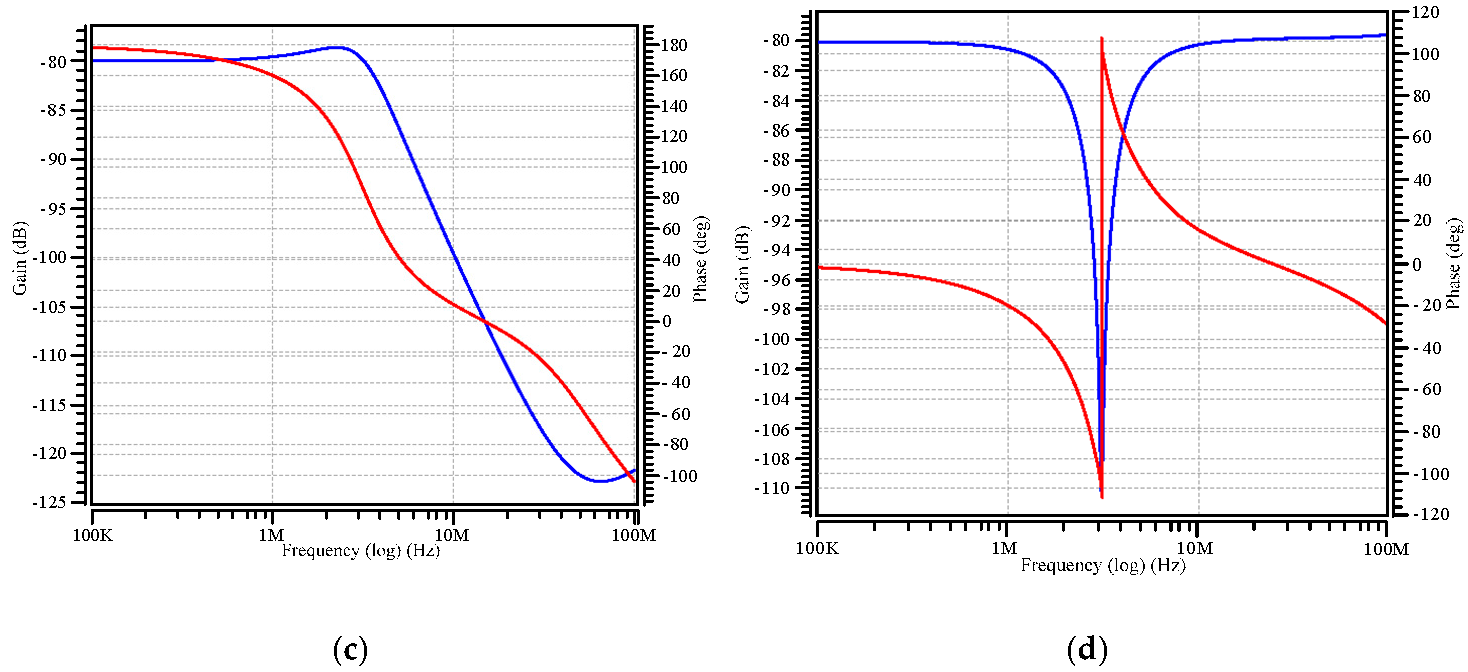
3. Simulation Results

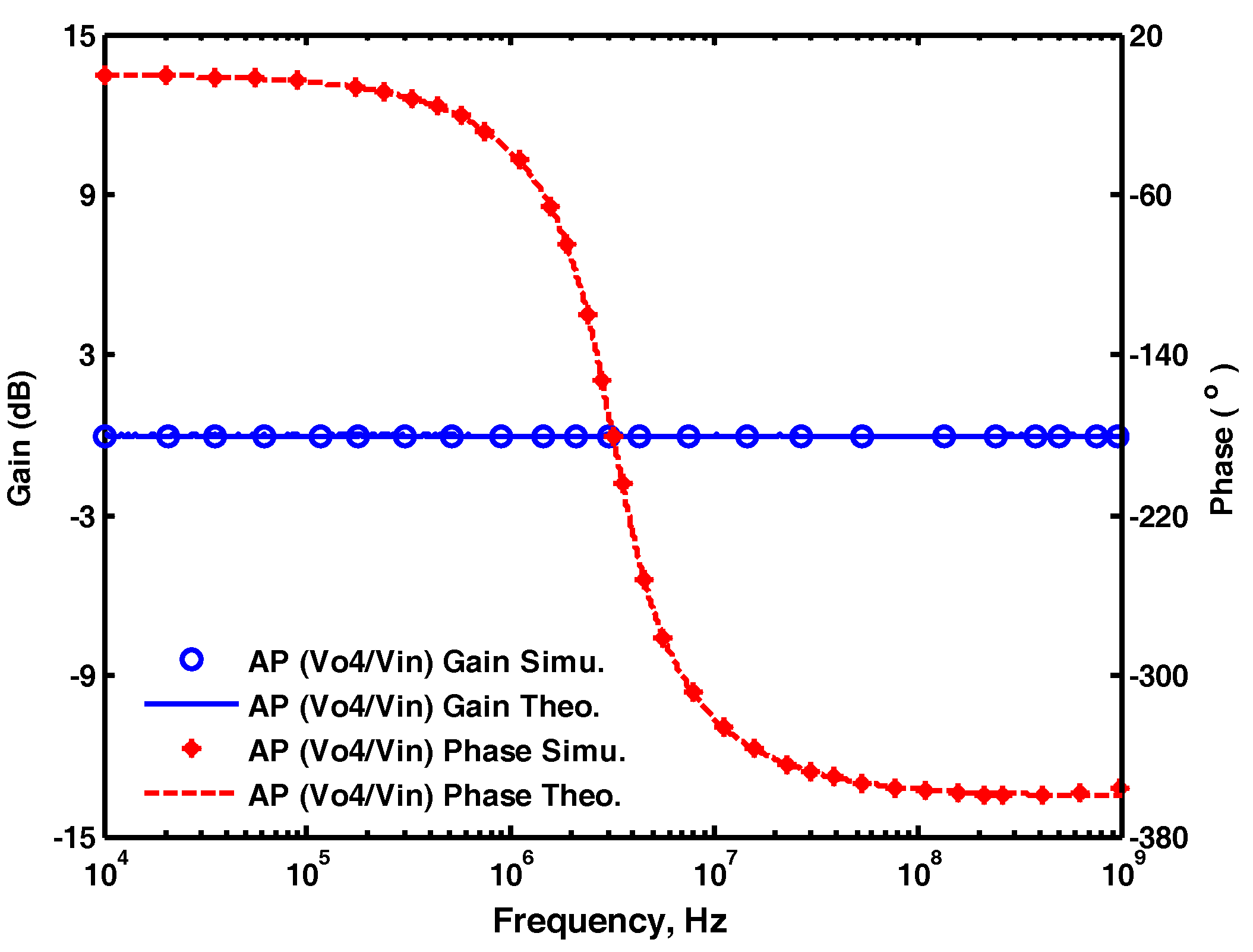
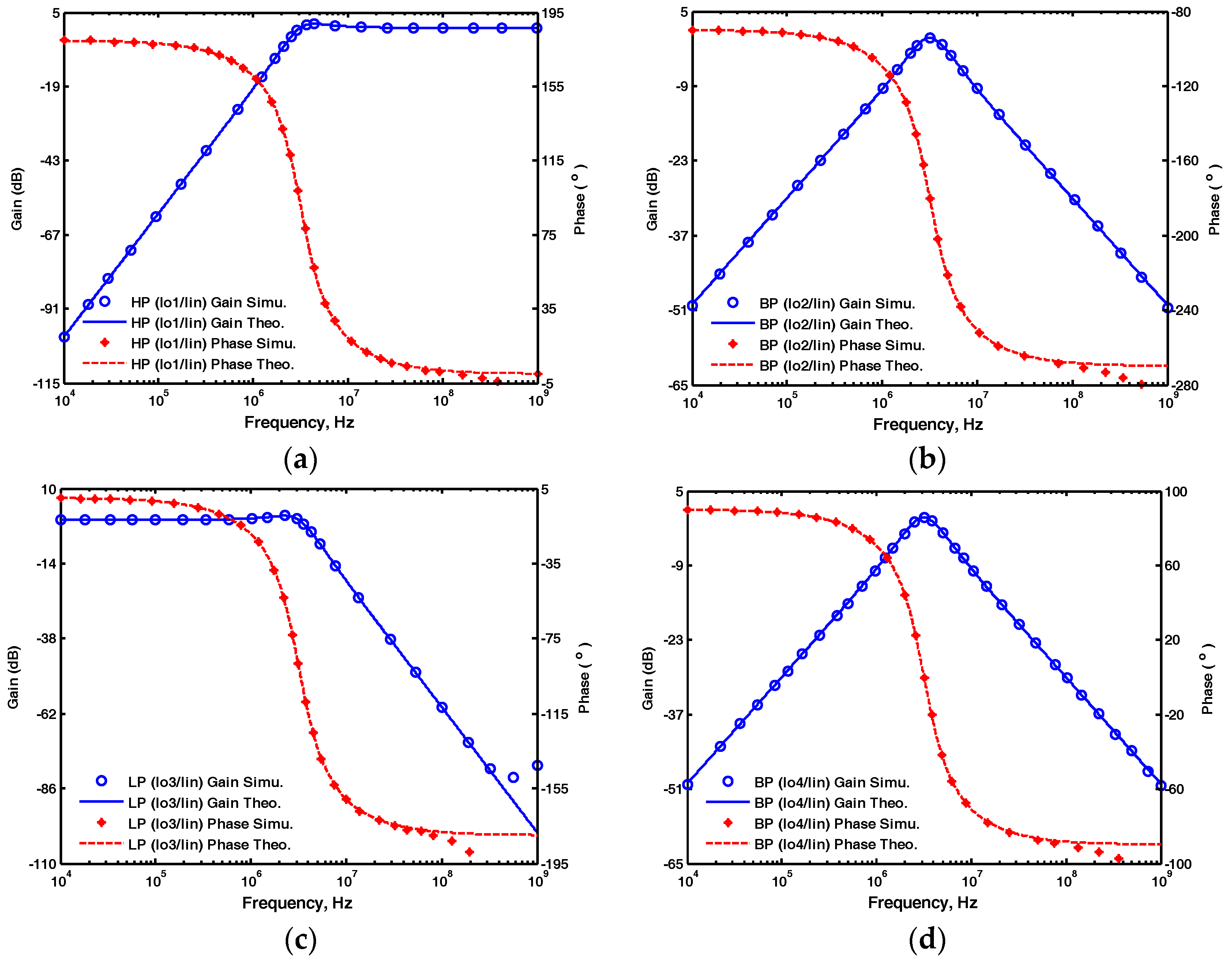
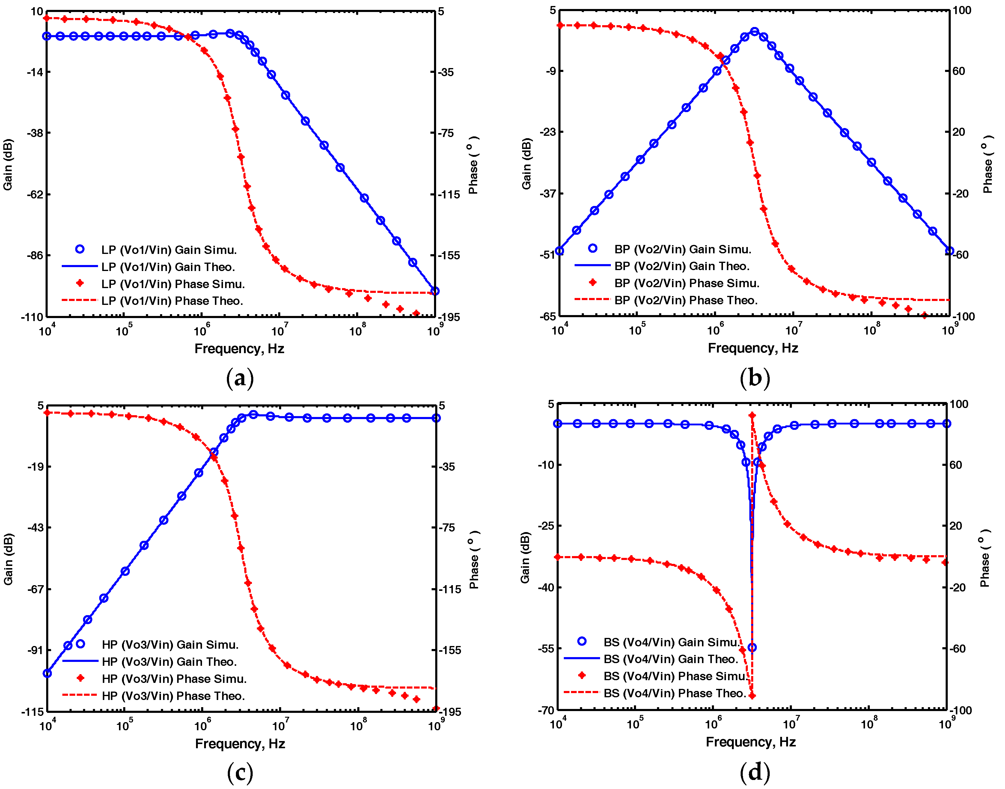
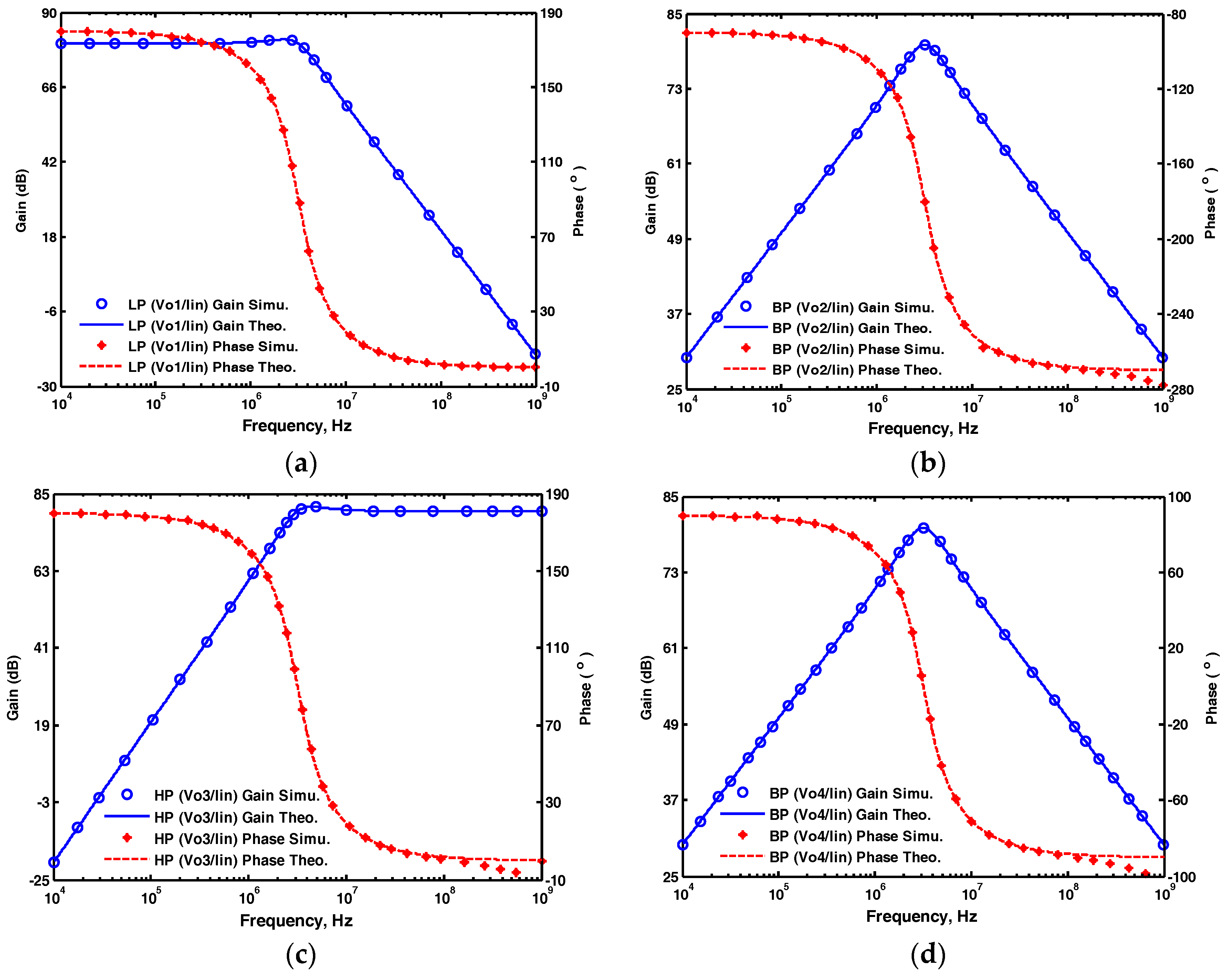
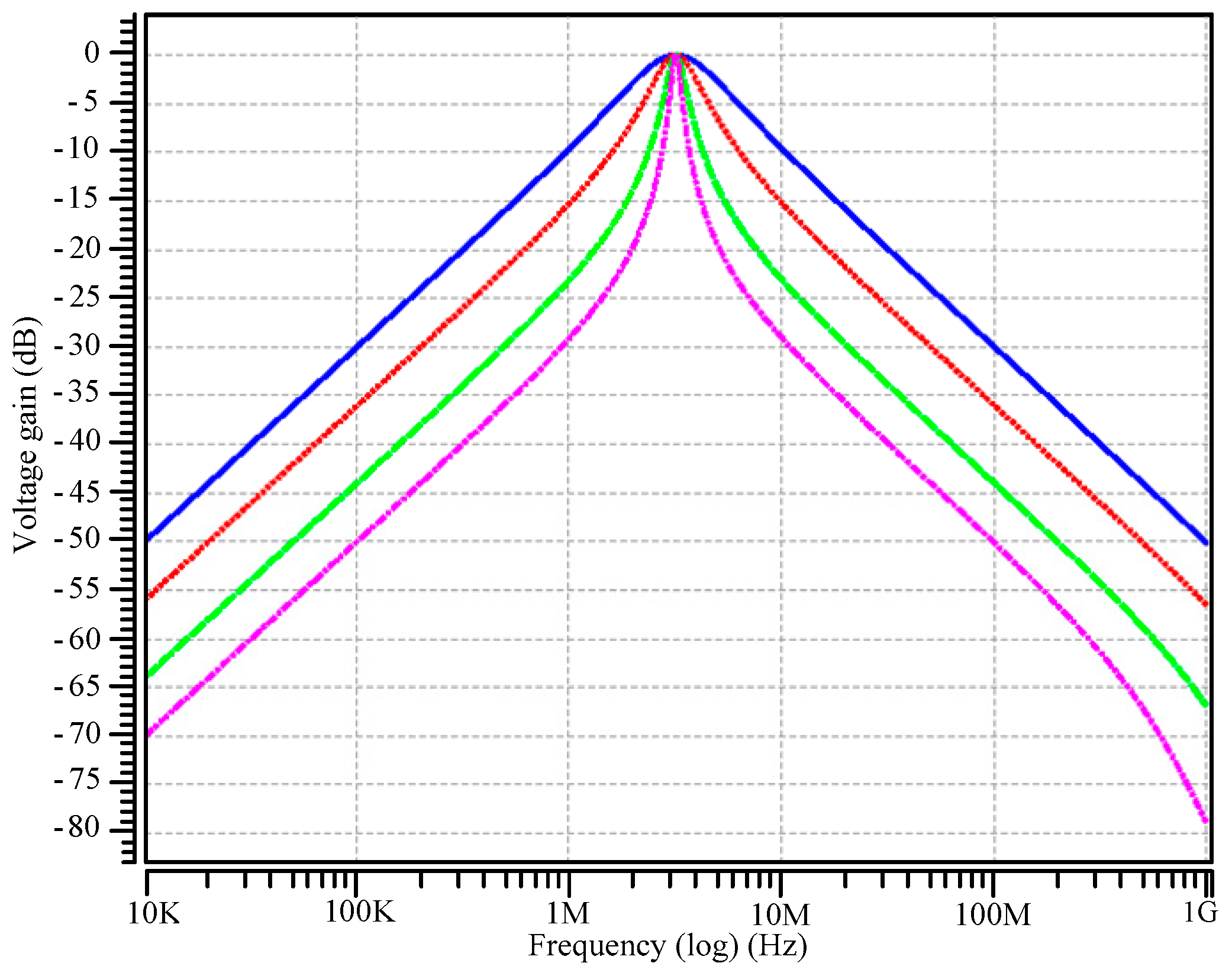
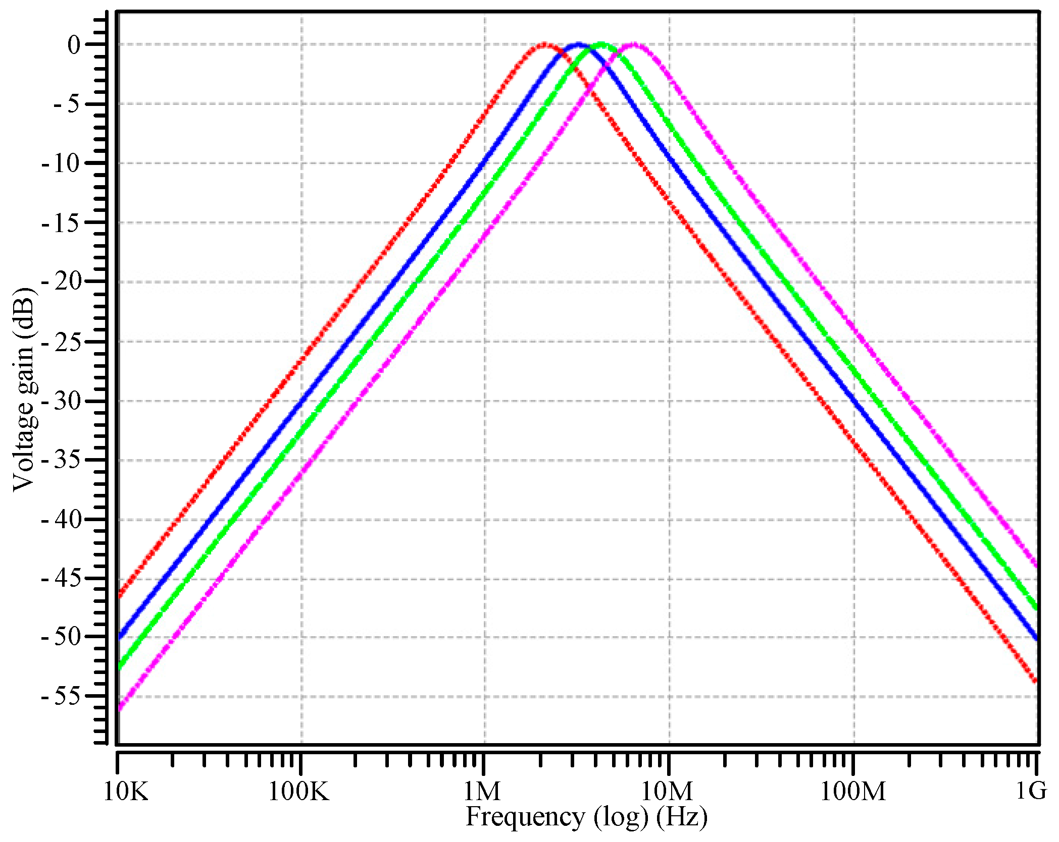
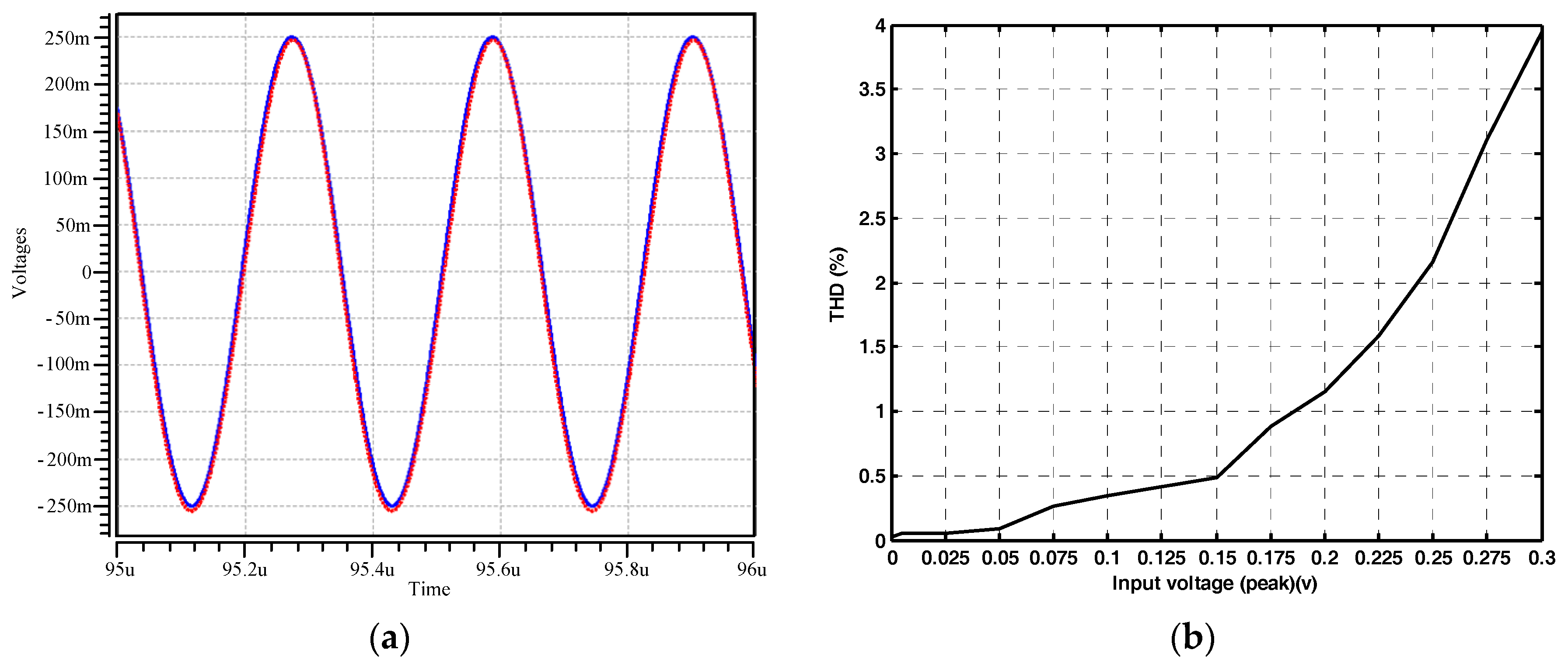
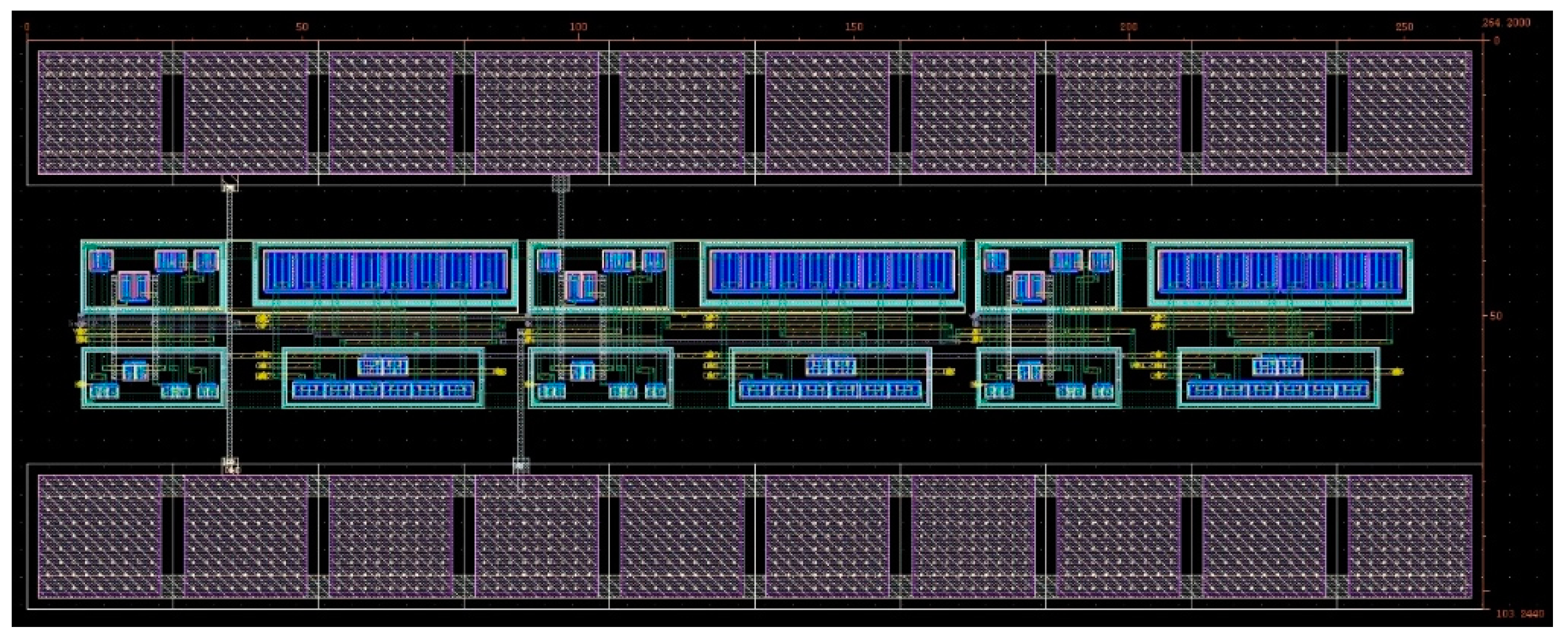
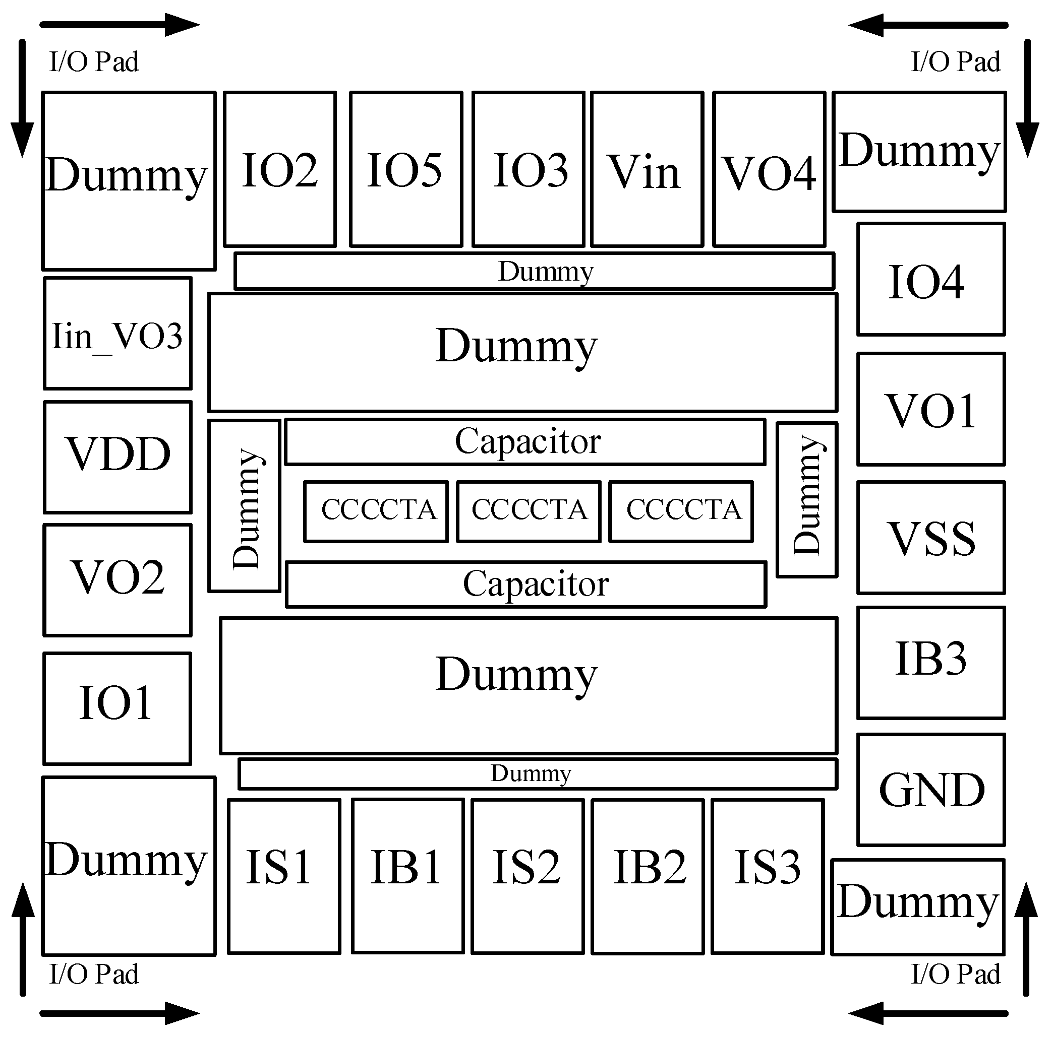
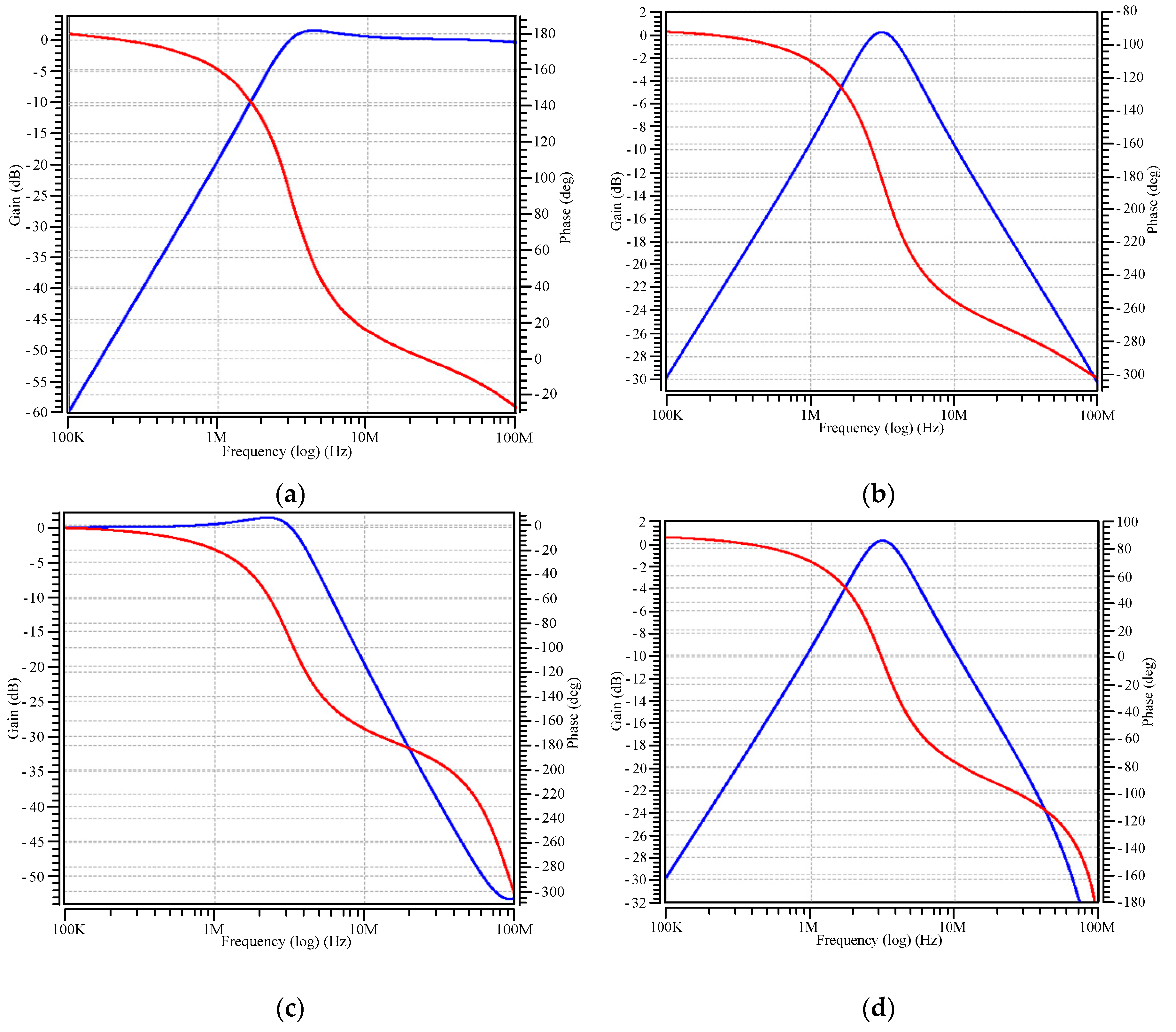
3.1. Pre-Layout Simulation

The performance of the proposed circuit was evaluated by an H-Spice simulation in a Taiwan Semiconductor Manufacturing Company (TSMC) 0.18-μm process. Figure 4 shows the complementary metal oxide semiconductor (CMOS) implementation of a CCCCTA [29]. The multiple current outputs are easily implemented by simply adding output branches. Table 6 gives the dimensions of the metal oxide semiconductor (MOS) transistors used in the CCCCTA implementation. The supply voltages are VDD = −VSS = 0.9 V. To obtain a pole frequency of fo = 3.183 MHz at Q = 1, the active and passive components were set to IB1 = IB2 = IB3 = 24.135 μA (gm = 100 μS), IS1 = IS2 = IS3 = 1.778 μA (RX = 10 kΩ) and C1 = C2 = 5 pF. Figure 5 represents the simulated frequency responses for the HP (Io1), BP (Io2), LP (Io3) and BP (Io4) filters in the CM. Figure 6 represents the simulated frequency responses for the LP (Vo1), BP (Vo2), HP (Vo3) and BS (Vo4) filters, respectively, in the VM. Figure 7 represents the VM non-inverting AP (Vo4) simulated frequency response when the output current signal Io5 is connected to the output voltage node Vo4. Figure 8 represents the simulated frequency responses for the HP, BP, LP and BS filters in the TAM. Figure 9 represents the simulated frequency responses for the LP, BP, HP and BS filters in the TIM. Figure 10 represents VM gain responses of BP (Vo2) filter for different IB1 and IS3 values, by keeping IB2 = IB3 = 24.135 μA, IS1 = IS2 = 1.778 μA and C1 = C2 = 5 pF. The Q varied (1, 2, 5 and 10) when fo was maintained at 3.183 MHz. Table 7 gives the different IB1 and IS3 values used in Figure 10. The Table 7 shows that Q can be used to adjust the input bias current IB1 without affecting the fo as depicted in Equation (18) and that the BP (Vo2) transfer gains can be independently controlled by changing IS3 without affecting the fo. Figure 11 represents the VM gain responses of the BP filter. The IB and IS values were changed by maintaining a constant ratio for constant Q. Table 8 shows the component values and corresponding ideal and simulated pole frequencies. The calculation results show that the fo can be adjusted without affecting the Q. The input dynamic range of the VM filter was tested by repeating the simulation for a sinusoidal input signal at fo = 3.183 MHz. Figure 12a shows the input dynamic range of the BP filter at the Vo2 output terminal with IB1 = IB2 = IB3 =96.5 μA (gm = 200 μS), IS1 = IS2 = IS3 = 7.113 μA (RX = 5 kΩ) and C1 = C2 = 10 pF, which extended to an amplitude of 0.5 V (peak to peak) without signification distortion. In Figure 12a, the percentage of total harmonic distortion (THD) is 2.16%, and the total power dissipation is 1.99 mW. The dependence of the output harmonic distortion on input voltage amplitude is illustrated in Figure 12b.

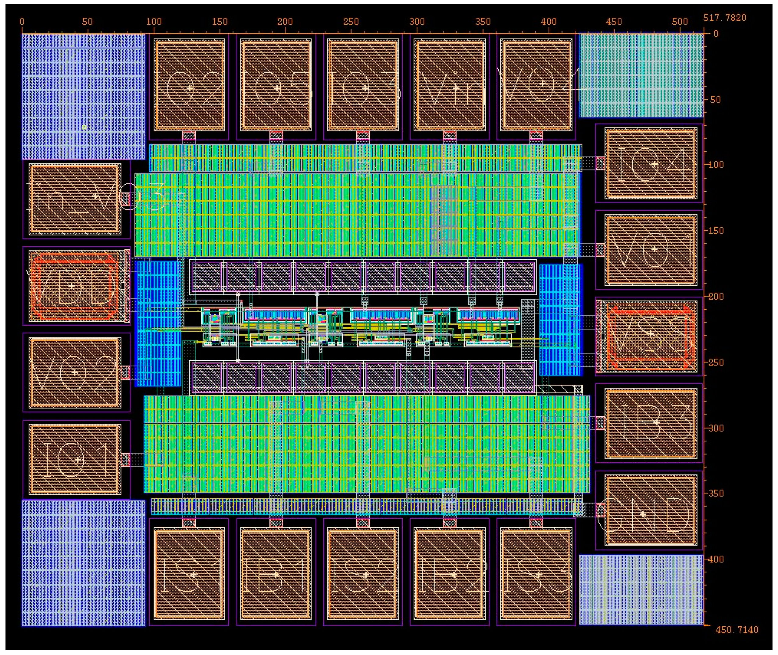
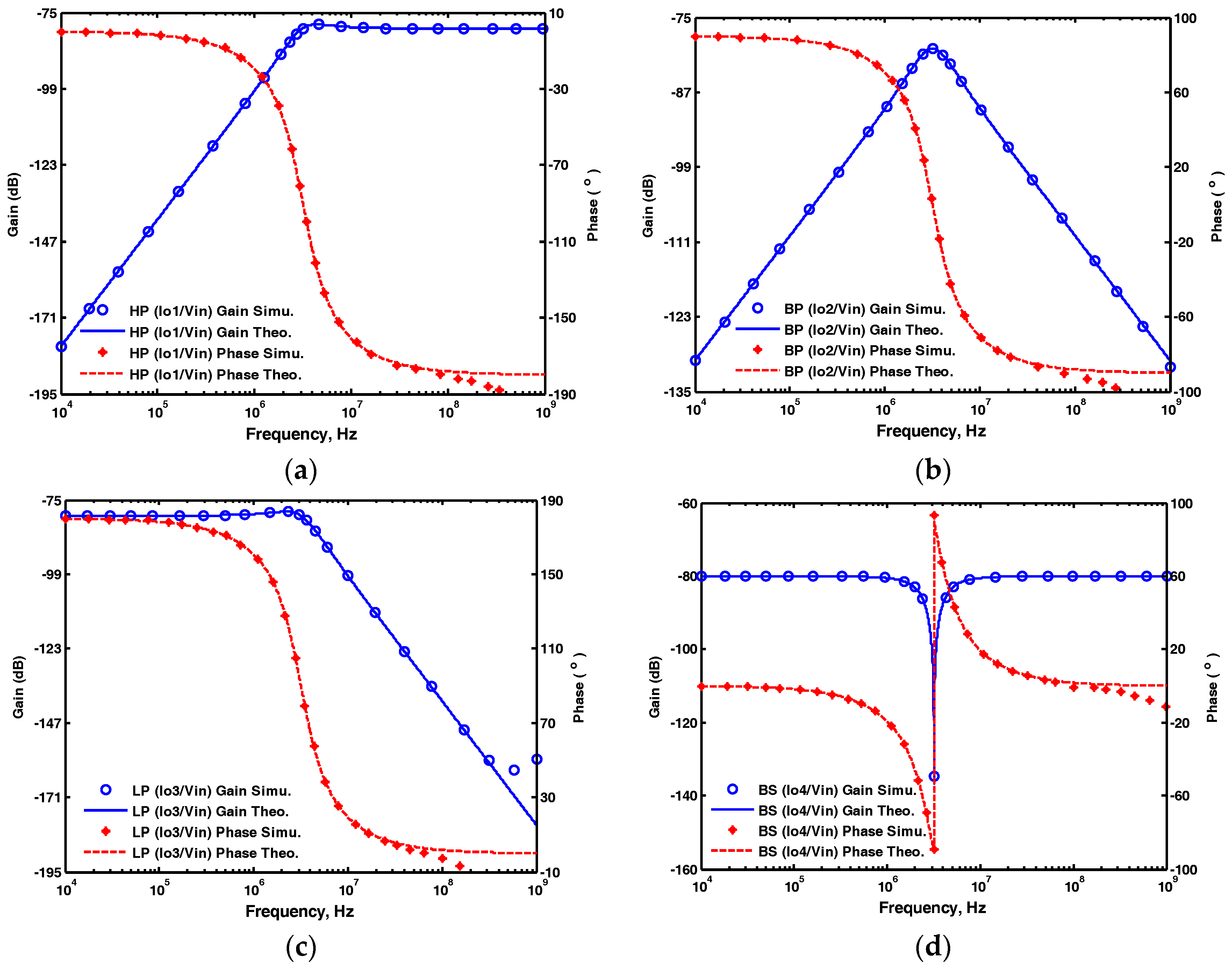
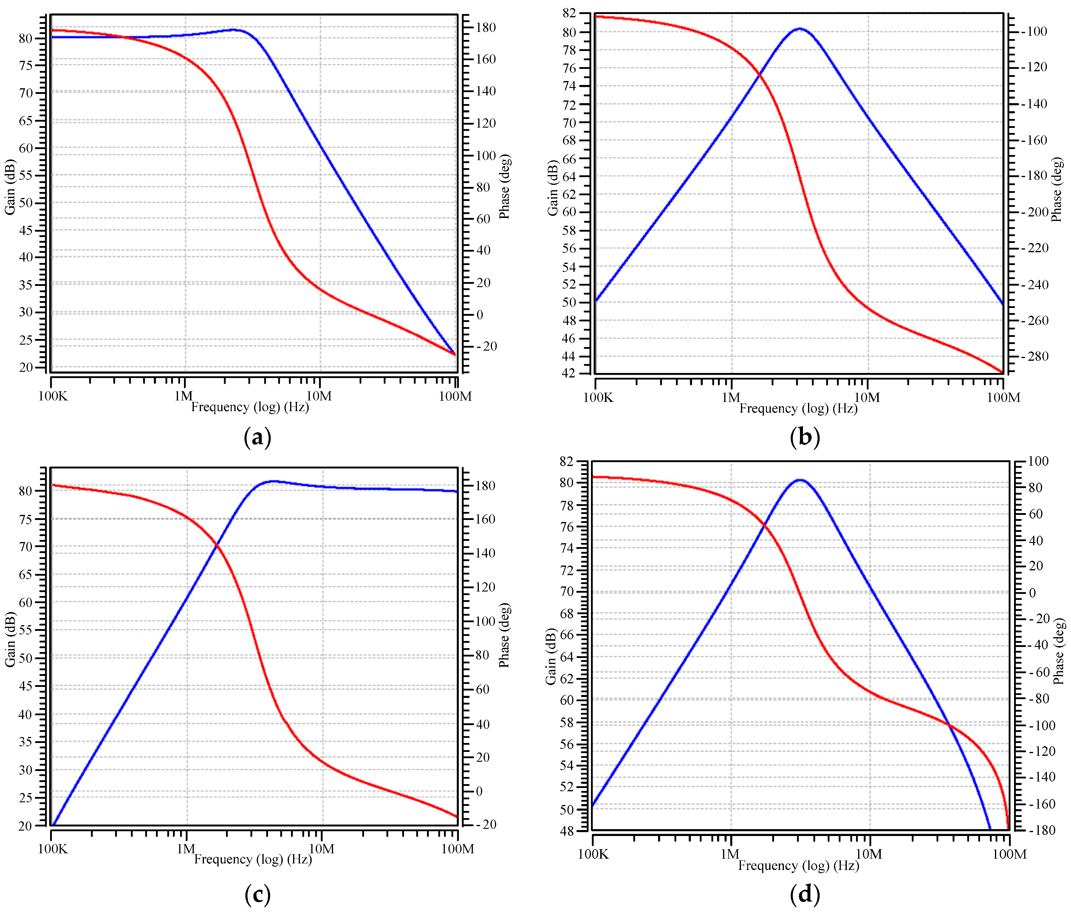
3.2. Post-Layout Simulation

The layout of the entire schematic was done using cadence’s virtuoso tool. Figure 13 and Figure 14 show the overall chip layout and the detail layout of the filter core, respectively. The layout floorplan is shown in Figure 15 which explains element placement. The component values of Figure 13 and Figure 14 were given by gm = 100 μS, RX = 10 kΩ and C1 = C2 = 5 pF, leading to a center frequency fo = 3.183 MHz. A design rules check (DRC) and a layout versus schematic (LVS) comparison were performed on the layout. The DRC checks for potential errors in the layout. The LVS checks the layout against the schematic and verifies that all the nets are matching. After the DRC and LVS were completed successfully, layout extraction was done. The extraction gives an overall idea about the parasitics of the design. All these processes are carried out using a cadence virtuoso schematic and layout editor tool for TSMC 0.18-μm CMOS process technology. The post-layout simulations were carried out to check the functionality of the design. Figure 16 represents the post-layout simulated frequency responses for the HP (Io1), BP (Io2), LP (Io3) and BP (Io4) filters in the CM. The post-layout simulation results show the CM simulated natural frequency as 3.10 MHz, that is, an approximately 2.52% error with the theoretical value. Figure 17 represents the post-layout simulated frequency responses for the LP (Vo1), BP (Vo2), HP (Vo3) and BS (Vo4) filter in the VM. The post-layout simulation results show the VM simulated natural frequency as 3.08 MHz, that is, an approximately 3.14% error with the theoretical value. Figure 18 represents the post-layout simulated frequency responses for the HP (Io1), BP (Io2), LP (Io3) and BS (Io4) filter in the TAM. The post-layout simulation results show the TAM simulated natural frequency as 3.10 MHz, that is, an approximately 2.52% error with the theoretical value. Figure 19 represents the post-layout simulated frequency responses for the LP (Vo1), BP (Vo2), HP (Vo3) and BP (Vo4) filter in the TIM. The post-layout simulation results show the TIM simulated natural frequency as 3.09 MHz, that is, an approximately 2.83% error with the theoretical value. It appears from Figure 16, Figure 17, Figure 18 and Figure 19 that the filter post-layout simulation performs all the filter functions well, but the small departures filter responses mainly stems from the parasitic impedance effects and non-ideal gains of the CCCCTA. The total power dissipation is found to be 0.593 mW. The chip area without pads is only 0.5177 × 0.4507 mm2.

4. Conclusions

This paper presents a new CCCCTA-based electronically tunable mixed-mode biquadratic filter, which uses three CCCCTAs and two grounded capacitors. When operating in CM/TAM, the circuit can simultaneously realise LP, BP and HP filtering responses. The BS/AP filtering responses are also obtained with the interconnection of the relevant output currents without any component-matching conditions. When operating in TIM, the circuit can simultaneously realise LP, HP and two BP filtering responses. The LP, BP, HP and BS/AP filtering responses are also obtained simultaneously in VM operation. The proposed circuit has the following nine advantages simultaneously: (1) resistorless and electronically tunable structure; (2) simultaneous realisation of three generic filtering responses in all the four possible modes; (3) capability to realise BS and AP filtering responses in the VM, CM and TAM without critical component-matching conditions; (4) low-input and high-output impedances for current signals; (5) high-input impedance for voltage signal; (6) use of only grounded capacitors; (7) orthogonal control of the parameters Q and ωo of the filter; (8) independent control of the VM filter gains without affecting the parameters Q and ωo; and (9) low active and passive sensitivity performances. The pre-layout simulation and post-layout simulation results in this study were consistent with the theoretical assumptions.

Acknowledgments

The authors would like to thank the reviewers and academic editor for their suggestions to improve the manuscript. Technical support from the National Chip Implementation Center (CIC) is also gratefully acknowledged.

Author Contributions

Hua-Pin Chen and Wan-Shing Yang conceived and designed the theoretical verifications; the optimization ideas were provided by Wan-Shing Yang; Hua-Pin Chen analysed the results and wrote the paper.

Conflicts of Interest

The authors declare no conflict of interest.

References

  1. Wilson, B. Recent developments in current conveyors and current-mode circuits. IEE Proc. G Circuits Devices Syst. 1990, 137, 63–77. [Google Scholar] [CrossRef]
  2. Schmid, H. Why “current mode” does not guarantee good performance. Analog Integr. Circuits Signal Process. 2003, 35, 79–90. [Google Scholar] [CrossRef]
  3. Cicekoglu, O.; Tarim, N.; Kuntman, H. Wide dynamic range high output impedance current-mode multifunction filters with dual-output current conveyors. AEU Int. J. Electron. Commun. 2002, 56, 55–60. [Google Scholar] [CrossRef]
  4. Chang, C.M.; Al-Hashimi, B.M.; Rose, J.N. Unified active filter baquad structures. IEE Proc. Circuits Devices Syst. 2004, 151, 273–277. [Google Scholar] [CrossRef]
  5. Maheshwari, S. High input impedance VM-APSs with grounded passive elements. IET Circuits Devices Syst. 2007, 1, 72–78. [Google Scholar] [CrossRef]
  6. Maheshwari, S. High output impedance current-mode all-pass sections with two grounded passive components. IET Circuits Devices Syst. 2008, 2, 234–242. [Google Scholar] [CrossRef]
  7. Hwang, Y.S.; Liu, W.H.; Tu, S.H.; Chen, J.J. New building block: Multiplication-mode current conveyor. IET Circuits Devices Syst. 2009, 3, 41–48. [Google Scholar] [CrossRef]
  8. Maheshwari, S. Analogue signal processing applications using a new circuit topology. IET Circuits Devices Syst. 2009, 3, 106–115. [Google Scholar] [CrossRef]
  9. Maheshwari, S.; Mohan, J.; Chauhan, D.S. Voltage-mode cascadable all-pass sections with two grounded passive components and one active element. IET Circuits Devices Syst. 2010, 4, 113–122. [Google Scholar] [CrossRef]
  10. Maheshwari, S.; Chaturvedi, B. High-input low-output impedance all-pass filters using one active element. IET Circuits Devices Syst. 2012, 6, 103–110. [Google Scholar] [CrossRef]
  11. Abdalla, K.K.; Bhaskar, D.R.; Senani, R. Configuration for realizing a current-mode universal filter and dual-mode quadrature single resistor controlled oscillator. IET Circuits Devices Syst. 2012, 6, 159–167. [Google Scholar] [CrossRef]
  12. Ibrahim, M.A.; Minaei, S.; Kuntman, H. A 22.5 MHz current-mode KHN-biquad using differential voltage current conveyor and grounded passive elements. Int. J. Electron. Commun. 2005, 59, 311–318. [Google Scholar] [CrossRef]
  13. Abuelma’atti, M.T.; Bentrcia, A.; Al-Shahrani, S.M. A novel mixed-mode current-conveyor-based filter. Int. J. Electron. 2004, 91, 191–197. [Google Scholar] [CrossRef]
  14. Pandey, N.; Paul, S.K.; Bhattacharyya, A.; Jain, S.B. A new mixed mode biquad using reduced number of active and passive elements. IEICE Electron. Express 2006, 3, 115–121. [Google Scholar] [CrossRef]
  15. Singh, V.K.; Singh, A.K.; Bhaskar, D.R.; Senani, R. Novel mixed-mode universal biquad configuration. IEICE Electron. Express 2005, 2, 548–553. [Google Scholar] [CrossRef]
  16. Minaei, S.; Ibrahim, M.A. A mixed-mode KHN-biquad using DVCC and grounded passive elements suitable for direct cascading. Int. J. Circuits Theory Appl. 2009, 37, 793–810. [Google Scholar] [CrossRef]
  17. Liao, W.B.; GU, J.C. SIMO type universal mixed-mode biquadratic filter. Indian J. Eng. Mater. Sci. 2011, 18, 443–448. [Google Scholar]
  18. Lee, C.N.; Chang, C.M. Single FDCCII-based mixed-mode biquad filter with eight outputs. AEU Int. J. Electron. Commun. 2009, 63, 736–742. [Google Scholar] [CrossRef]
  19. Shah, N.A.; Malik, M.A. Multifunction mixed-mode filter using FTFNs. Analog Integr. Circuits Process. 2006, 47, 339–343. [Google Scholar] [CrossRef]
  20. Abuelma’atti, M.T.; Bentrcia, A. A novel mixed-mode OTA-C universal filter. Int. J. Electron. 2005, 92, 375–383. [Google Scholar] [CrossRef]
  21. Chen, H.P.; Liao, Y.Z.; Lee, W.T. Tunable mixed-mode OTA-C universal filter. Analog Integr. Circuits Process. 2009, 58, 135–141. [Google Scholar] [CrossRef]
  22. Lee, C.N. Multiple-mode OTA-C universal biquad filters. Circuits Syst. Signal Process. 2010, 29, 263–274. [Google Scholar] [CrossRef]
  23. Pandey, N.; Paul, S.K. Mixed-mode universal filter. J. Circuits Syst. Comput. 2013, 22, 1250064. [Google Scholar] [CrossRef]
  24. Li, Z.J. Mixed-mode universal filter using MCCCII. AEU Int. J. Electron. Commun. 2009, 63, 1072–1075. [Google Scholar]
  25. Pandey, N.; Paul, S.K. SIMO mixed mode universal filter. J. Act. Passiv. Eletron. Devices 2012, 7, 215–226. [Google Scholar]
  26. Maheshwari, S.; Singh, S.V.; Chauhan, D.S. Electronically tunable low-voltage mixed-mode universal biquad filter. IET Circuits Devices Syst. 2011, 5, 149–158. [Google Scholar] [CrossRef]
  27. Singh, S.V.; Maheshwari, S.; Chauhan, D.S. Novel electronically tunable mixed-mode biqaud filter. In Electronics and Signal Processing, Lecture Notes in Electrical Engineering (LNEE); Springer: Berlin/Heidelberg, Germany, 2011; Volume 97, pp. 735–742. [Google Scholar]
  28. Siripruchyanun, M.; Jaikla, W. Current controlled current conveyor transconductance amplifier (CCCCTA): A building block for analog signal processing. Electr. Eng. 2008, 9, 443–455. [Google Scholar] [CrossRef]
  29. Jaikla, W.; Siripongdee, S.; Suwanjan, P. MISO current-mode biquad filter with independent control of pole frequency and quality factor. Radioengineering 2012, 21, 886–891. [Google Scholar]
Figure 1. CCCCTA (current controlled current conveyor transconductance amplifier) symbolic representation.
Applsci 07 00244 g001
Figure 2. Proposed electronically tunable mixed-mode biquadratic filter.
Applsci 07 00244 g002
Figure 3. Non-ideal equivalent circuit model of the CCCCTA.
Applsci 07 00244 g003
Figure 4. Complementary metal oxide semiconductor (CMOS) realization of the CCCCTA [29].
Applsci 07 00244 g004
Figure 5. The CM-simulated frequency responses of Figure 2 (a) highpass filter; (b) bandpass filter; (c) lowpass filter; and (d) bandpass filter.
Applsci 07 00244 g005
Figure 6. The VM-simulated frequency responses of Figure 2 (a) lowpass filter; (b) bandpass filter; (c) highpass filter; and (d) bandstop filter.
Applsci 07 00244 g006
Figure 7. The VM-simulated allpass filter frequency responses of Figure 2.
Applsci 07 00244 g007
Figure 8. The TAM-simulated frequency responses of Figure 2 (a) highpass filter; (b) bandpass filter; (c) lowpass filter; and (d) bandstop filter.
Applsci 07 00244 g008
Figure 9. The TIM-simulated frequency responses of Figure 2 (a) lowpass filter; (b) bandpass filter; (c) highpass filter; and (d) bandpass filter.
Applsci 07 00244 g009
Figure 10. The VM bandpass filter at the output Vo2 of Figure 2 when variation in Q with fo fixed at 3.183 MHz (Q = 1: blue; Q = 2: red; Q = 5: green; and Q = 10: pink).
Applsci 07 00244 g010
Figure 11. The VM bandpass filter at the output Vo2 of Figure 2 when variation in fo with Q fixed at 1 (fo = 2.13 MHz: red; fo = 3.22 MHz: blue; fo = 4.32 MHz: green; and fo = 6.48 MHz: pink).
Applsci 07 00244 g011
Figure 12. Time-domain results of VM bandpass filter at the output Vo2 of Figure 2 (a) input (blue line) and output (red line) waveforms; (b) total harmonic distortion (THD) analysis results on input voltage at 3.183 MHz.
Applsci 07 00244 g012
Figure 13. The layout of the proposed mixed-mode biquadratic filter chip.
Applsci 07 00244 g013
Figure 14. The core of the proposed mixed-mode biquadratic filter.
Applsci 07 00244 g014
Figure 15. The layout floorplan.
Applsci 07 00244 g015
Figure 16. The CM post-layout gain (blue line) and phase (red line) simulation responses (a) highpass filter (Io1/Iin); (b) bandpass filter (Io2/Iin); (c) lowpass filter (Io3/Iin),; and (d) bandpass filter (Io4/Iin).
Applsci 07 00244 g016
Figure 17. The VM post-layout gain (blue line) and phase (red line) simulation responses (a) lowpass filter (Vo1/Vin); (b) bandpass filter (Vo2/Vin); (c) highpass filter (Vo3/Vin); and (d) bandstop filter (Vo4/Vin).
Applsci 07 00244 g017
Figure 18. The TAM post-layout gain (blue line) and phase (red line) simulation responses (a) highpass filter (Io1/Vin); (b) bandpass filter (Io2/Vin); (c) lowpass filter (Io3/Vin); and (d) bandstop filter (Io4/Vin).
Applsci 07 00244 g018aApplsci 07 00244 g018b
Figure 19. The TIM post-layout gain (blue line) and phase (red line) simulation responses (a) lowpass filter (Vo1/Iin); (b) bandpass filter (Vo2/Iin); (c) highpass filter (Vo3/Iin); and (d) bandpass filter (Vo4/Iin).
Applsci 07 00244 g019
Table 1. Comparison of previously reported mixed-mode filters. 1
FiltersNo. of Active ElementsNo. of Passive ElementsComposed of Equivalent Active Elements
[13]7 CCII2C + 8R7 CCII
[14]3 CCII3C + 4R + 2 switch3 CCII
[15]4 CFOA2C + 9R + 1 switch4 CFOA
[16]3 DVCC2C + 3R3 DVCC
[17]3 DDCC2C + 4R3 DDCC
[18]1 FDCCII2C + 3R2 DDCC
[19]3 FTFN2C + 3R3 × 2 CFOA
[20]7 OTA2C7 OTA
[21]5 OTA2C5 OTA
[22]4 OTA2C4 OTA
[23]4 MOCCCII2C4 MOCCCII
[24]5 MOCCCII2C5 MOCCCII
[25]4 MOCCCII2C4 MOCCCII
[26]3 CCCCTA2C3 × (1 CCCII + 1 OTA)
[27]3 CCCCTA2C3 × (1 CCCII + 1 OTA)
this work3 CCCCTA2C3 × (1 CCCII + 1 OTA)
1 CCII: current conveyor; CFOA: current feedback operational amplifier; DVCC: differential voltage current conveyor; FDCCII: fully differential current conveyor; FTFN: four-terminal floating nullor; OTA: operational transconductance amplifier; MOCCCII: multiple-output current controlled conveyor; CCCCTA: current controlled current conveyor transconductance amplifier.
Table 2. Characteristic comparisons with previous reported mixed-mode filters.
FiltersProperties 1
(1)(2)(3)(4)(5)(6)(7)(8)(9)
[13]nononononoyesyesyesyes
[14]nononononoyesnoyesyes
[15]nononononoyesnoyesyes
[16]nononoyesyesyesyesnoyes
[17]noyesnononoyesyesnoyes
[18]nononononoyesyesnono
[19]nonononononononoyes
[20]yesnononoyesyesyesyesyes
[21]yesnononoyesyesyesnoyes
[22]yesnononoyesyesnonoyes
[23]yesnonoyesyesyesnonoyes
[24]yesyesnononoyesyesnoyes
[25]yesyesnoyesnoyesnonoyes
[26]yesyesnonoyesyesnonoyes
[27]yesyesnoyesyesyesyesnoyes
this workyesyesyesyesyesyesyesyesyes
1 (1) resistorless and electronically tunable structure; (2) simultaneous realisation of three generic filtering responses in all the four possible modes; (3) capability to realise bandstop and allpass filtering responses in the voltage mode, current mode and transadmittance mode without critical component-matching conditions; (4) low-input and high-output impedances for current signals; (5) high-input impedance for voltage signal; (6) use of only grounded capacitors; (7) orthogonal control of the parameters quality factor (Q) and resonance angular frequency (ωo) of the filter; (8) independent control of the voltage mode filter gains without affecting the parameters Q and ωo; and (9) low active and passive sensitivity performances.
Table 3. Comparison of the proposed circuit with previously reported single-input-type of electronically tunable CCCCTA-based mixed-mode filters [26,27]. 1
Related WorksNo. of Active ElementsFilter Function RealizationThe ωo and Q Orthogonal TunabilityIndependent Tunability VM Filter Gains without Affecting ωo and Q
CMVMTAMTIM
[26]3All fiveLP, BP, HPAll fiveLP, BP, HPnono
[27]3All fiveLP, BP, BSAll fiveLP, BP, BSyesno
this work3All fiveAll fiveAll fiveLP, BP, HPyesyes
1 ωo: resonance angular frequency; Q: quality factor; CM: current mode; VM: voltage mode; TAM: transadmittance mode; TIM: transimpedance mode; LP: lowpass; BP: bandpass; HP: highpass; BS: bandstop.
Table 4. Characteristic comparisons with previous works in [26,27]. 1
Related WorksMatching ConstraintsInput Voltage at High Input ImpedanceInput Current at Low Input ImpedanceOutput Current at High Output Impedance
[26]APyesnoyes
[27]APyesyesyes
this worknilyesyesyes
1 AP: allpass.
Table 5. Input conditions and various functions realised.
Filter functionVin = 0, Iin is Input SignalIin = 0, Vin is Input Signal
CMTIMVMTAM
HPIo1Vo3Vo3Io1
LPIo3Vo1Vo1Io3
BPIo2, Io4, Io5Vo2, Vo4Vo2Io2, Io5
BSIo1 + Io3---Vo4Io4
APIo1 + Io2 + Io3---Vo4 *Io4 + Io5
* A non-inverting AP voltage-mode transfer function is easily obtained by connecting the output current signal Io5 to the output voltage node Vo4.
Table 6. The aspect ratios of the CMOS transistors in CCCCTA implementation.
TransistorsLength (µm)Width (µm)
M1–M20.185
M3–M40.188
M5–M110.185
M12–M190.183
M20–M210.510
M22–M290.825
M30–M350.88
Table 7. The different IB1 and IS3 values used to obtain a specified Q.
Bias Current IB1 (µA)Bias Current IS3 (µA)Quality Factor
24.1351.7782Q = 1
6.0350.4446Q = 2
0.9660.0712Q = 5
0.2410.0178Q = 10
Table 8. Component values used to obtain a specified fo.
Bias Currents IB1 = IB2 = IB3Bias Currents IS1 = IS2 = IS3Capacitances C1 = C2Calculated Value of foSimulated Value of foFrequency Error
10.726 µA
(gm = 66.67 µS)
0.79 µA
(RX = 15 kΩ)
5 pF2.122 MHz2.13 MHz0.3%
24.135 µA
(gm = 100 µS)
1.7782 µA
(RX = 10 kΩ)
5 pF3.183 MHz3.22 MHz1.62%
42.902 µA
(gm = 133.33 µS)
3.161 µA
(RX = 7.5 kΩ)
5 pF4.244 MHz4.32 MHz1.79%
96.5 µA
(gm = 200 µS)
7.113 µA
(RX = 5 kΩ)
5 pF6.366 MHz6.48 MHz1.79%

