
Mode Coupling Properties of the Plasmonic Dimers Composed of Graphene Nanodisks
by
 , ,
, ,
Houbo Chen
1, 
Weibin Qiu
1,*,
Pingping Qiu
1,
Junbo Ren
1,
Zhili Lin
1,
Jia-Xian Wang
1,
Qiang Kan
2 and
Jiao-Qing Pan
2 1
Fujian Key Laboratory of Light Propagation and Transformation, College of Information Science and Engineering, Huaqiao University, No. 668, Jimei Avenue, Jimei District, Xiamen 361021, China
2
Institute of Semiconductors, Chinese Academy of Sciences, 35A, Qinghua East Road, Haidian District, Beijing 100086, China
*
Author to whom correspondence should be addressed.
Appl. Sci. 2017, 7(4), 359; https://doi.org/10.3390/app7040359
Submission received: 16 January 2017
/
Revised: 28 March 2017
/
Accepted: 30 March 2017
/
Published: 5 April 2017
(This article belongs to the Section Optics and Lasers)
Abstract
:The electromagnetic properties of the plasmonic dimer composed of coupled graphene nanodisks are numerically investigated in this paper. The results demonstrate that the degeneracy of the plasmonic modes of the dimer is lifted when the coupling is introduced. The evolution of the plasmonic mode, with the variation of inter-disk distance and the chemical potential of one of the nanodisks, is studied. The proposed structure might find broad areas of application including light–matter interaction, optical switching, directional emission of the plasmonic emitter, etc.
1. Introduction
Similar to electronic atom and molecule systems, photonic molecules (PhMs) and plasmonic molecules (PMs) are composed of interacting nanostructures in which the specific collective electromagnetic (EM) behaviors are demonstrated [1,2]. These behaviors include Fano resonance [3,4,5], slow light [6,7], EM-induced transparency [8,9,10] etc., which result from the coupling between the plasmons and the external disturbance. In the past decade, PhMs and PMs have found significant applications in broad areas including fundamental sciences, the processing of information and biochemics due to their excellent properties of high quality (Q) factors, flexible structure design, and high sensitivity to the variation of the environments [11]. Among the reported works, Qiang Li et al. [12] proposed and fabricated a hybrid photonic–plasmonic molecule composed of two coupled identical Ag-Al2O3-Si sandwich disks. This hybrid photonic–plasmonic molecule has sub-wavelength properties and provides a novel platform for the exploration of the light–matter interaction. Sang Wook Kim et al. [13] reported the energy-level evolution of coupled non-identical microdisks (CNMs), which were characterized by their avoided crossing which is intrinsically associated with the exceptional point or the non-Hermitian degeneracy. Svetlana V. Boriskina [14] analyzed the wavelength of the Q factors of the whispering-gallery (WG) modes in the PhM micro-disks as a function of the parameter of the PhM numerically, and demonstrated the crossing and avoid-crossing characteristics. However, all the above-mentioned micro or nanodisk based cavities were made by a conventional novel metal such as Ag and Au, or by dielectric materials such as SiO2. Thus, the huge ohmic loss would degrade the properties of the devices, for example, Q factors. Furthermore, frequency tunability is impossible as long as the geometric structures of the devices are determined. All the intrinsic shortcomings of the conventional plasmonic materials become an obstacle to practical application.
Recently, graphene, which is composed of a single layer of carbon atoms arranged in a two-dimensional (2D) honeycomb lattice, has attracted great attention in the fields of electronics and photonics all over the world due to its excellent material properties [15,16,17]. More specifically, in the field of the plasmonics, graphene offers the advantages of high confinement capability, low damping loss and tunability of working frequency. Consequently, graphene is a reliable material to substitute conventional metal materials in the field of plasmonics.
Zhu X. et al. investigated plasmon–phonon coupling in large-area graphene dot and antidot arrays [18]. Rosolen G. and Maes B. reported asymmetric and connected graphene dimers for a tunable plasmonic response [19]. Hadad Y. et al. showed that an electrically small chemical potential interruption in a graphene layer may possess a quasi-static resonance that launches a mixed-type semilocalized plasmon wave [20]. They also designed a system that is extremely sensitive to the quantized spectrum of graphene Landau levels and predicted up to 90° of Faraday rotation with just a single sheet of graphene [21]. We have proposed and numerically explored the plasmonic dimers composed of coupled graphene nanodisks of different sizes, which are surrounded by another chemical potential on the same piece of infinite graphene monolayer [22]. The split modes with non-degenerate wavelengths appear in the proposed structure. Further, the coupling between fundamental and first order WG modes has been pointed out. In the current work, we further analyze the field properties of the collective mode including the resonant frequency; the Q factor in a graphene plasmonic dimer with different chemical potentials in each nanodisk; and we discuss the physical principles behind the EM behaviors of the dimers. The proposed plasmonic molecules could find broad areas of application in fields including tunable filters [23], optical sensors [24] and optical switchers [25].
2. Models and Simulation Method
The 2D schematic of the plasmonic dimer molecule composed of graphene nanodisks is illustrated in Figure 1, where R is the radius of the nanodisks; g is the gap between the two nanodisks; the chemical potential of each nanodisk is μc2 and μc3, respectively. The chemical potential of the infinite area is μc1. Perfectly matched layer (PML) is employed as the boundary condition in order to avoid the reflected wave at the boundaries. In this article, the plasmonic properties of the dimers are investigated by utilizing the commercially available software COMSOL Multi-physics, RF module, eigen frequency solver. The graphene monolayer is modeled as an ultrathin film which can be characterized by the effective index defined as neff = β/k0, where k0 = 2π/λ is the wavenumber in free space [26]. The propagation constant of surface plasmon polaritons (SPPs) supported by monolayer graphene can be written as [27,28]
where η0 (377 Ω) is the intrinsic impedance of the air, which can be expressed by (μ0/ε0)1/2 where μ0 and ε0 represent the permeability and permittivity of vacuum, respectively. The surface conductivity of graphene σg, composed of the interband electron transitions σinter and the intraband electron–photon scattering σintra, is given by the Kubo formula [17,27,28,29],
with
where μc is the chemical potential of graphene; ω is the angular frequency of the plasmon; ћ is the reduced Planck’s constant; e is the electron charge; kB is the Boltzmann’s constant; T is the temperature; and τ is the electron momentum relaxation time. Specifically, the chemical potential of graphene is tunable by either chemical doping or external electrical gating locally [27,30]. Pioneering work showed that a chemical potential as high as 2 eV has been obtained experimentally [31]. Also, a relaxation time as high as 3ps has been achieved experimentally [32]. Thus, in this paper, a relaxation time less than 1ps and a chemical potential less than 1 eV are chosen, which are conservative enough to ensure the reliability of our calculation.
3. Results and Discussion
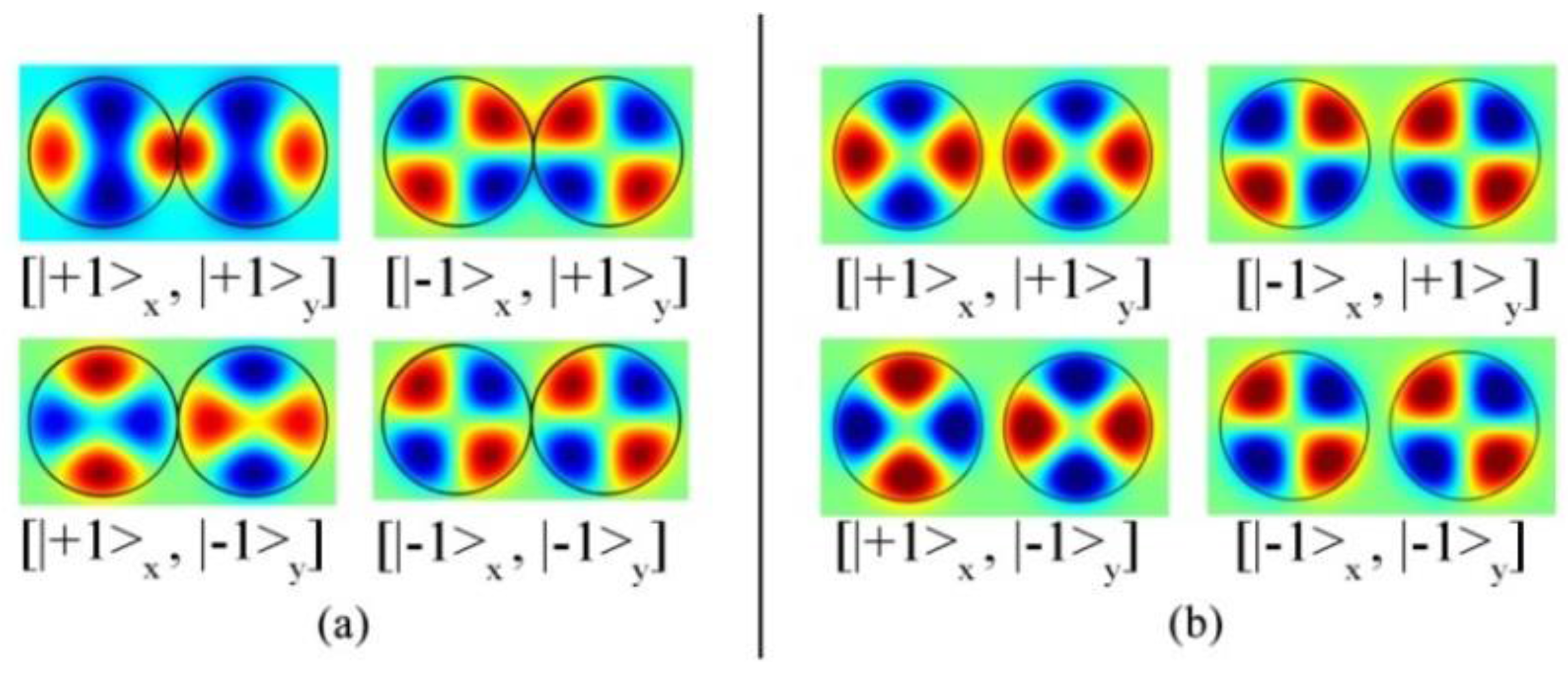
When two nanodisks approach each other, the EM fields of the plasmon interact, and the collective modes appear. First, we study the collective resonant EM mode field distribution as a function of the gap between the two nanodisks, where μc2 = μc3 = 0.5 eV, μc1 = 0.1 eV and R = 50 nm. The z component of the typical electric field distribution of TM2,1 modes of the dimer with a gap of 0 nm and 15 nm are illustrated in Figure 2a,b, respectively. According to the symmetry with respect to the X and Y directions, the four categories of the graphene plasmonic dimer modes are defined as [|+1>x,|+1>y], which is symmetric with respect to both the X and Y directions; [|+1>x,|−1>y], which is symmetric with respect to the X direction and anti-symmetric with respect to the Y direction; [|−1>x,|+1>y], which is anti-symmetric with respect to the X direction and symmetric with respect to the Y direction; and [|−1>x,|−1>y], which is anti-symmetric with respect to both the X and Y direction. More specifically, we follow Ref. [12] and regard the modes which are anti-symmetric with respect to the Y direction as the anti-bonding modes. Normally, the anti-bonding modes are located at the higher energy states. On the other hand, the modes that are symmetric with respect to the Y direction are regarded as the bonding modes, and are located at the lower energy states [12]. The frequency and the quality (Q) factor of the collective modes, as a function of the gap g, are plotted in Figure 3a,b, respectively. It is shown in Figure 3a that the frequencies of the anti-bonding modes decrease with the increasing of the gap g, while the counterparts of the bonding modes demonstrate the converse trend. The coupling strength between the WG modes of the nanodisks is indicated by the frequency splitting of the bonding or anti-bonding modes. When the gap g increases, the coupling strength between the plasmonic modes of the individual nanodisks degrades. Thus, the frequency splitting of the anti-bonding and the bonding modes decreases accordingly [12]. When g further increases to more than 50 nm, all the four mode categories combine together, the result of which is identical to the resonant mode of a single isolated nanodisk. This means that there is no interaction between the two nanodisks of the dimer.
It is also shown in Figure 3b that the Q factor of the collective plasmonic mode of the graphene dimer demonstrates an identical trend to that of the resonant frequency as a function of the gap g. To understand this behavior, we plot the real part and imaginary part of the propagation constant β as a function of frequency in Figure 4, where the chemical potential is 0.5 eV. In general, the Q factor is given by [33,34], where relates to the radiation loss and relates to the absorption loss. The radiation loss is determined by the radius and material of the cavity, and is calculated by
where Re(β) and |Im(β)| are the real part and the absolute value of the imaginary part of the propagation constant β. For a graphene sheet with a chemical potential of 0.5 eV, when the frequency of the plasmon increases from 80 THz to 83.5 THz, Re(β) and |Im(β)| increase together. However, the rising rate of Re(β) is even much faster than 2|Im(β)|. Consequently, the Q factor increases as the increasing of frequency, and finally results in a similar frequency trend as a function of given g, which are shown in Figure 3a,b.
Next, we investigate the frequency splitting ΔF of the corresponding anti-bonding and bonding modes as a function of the azimuthal mode number m of the plasmonic WG mode TMm,1 of the graphene dimers. Figure 5 shows the frequency splitting ΔF of bonding and anti-bonding of WG modes as a function of m, where the distance g is 5 nm. When the azimuthal number increases from 2 to 8, the frequency ΔF of the bonding mode decreases from 0.567 to 0.002 THz, while the counterpart of the anti-bonding mode decreases from 0.275 to 0.0002 THz. When the azimuthal number increases, the wavelength reduces. However, the EM field confinement capacity of the graphene dimer becomes stronger as the resonant wavelength decreases. So the coupling between the plasmonic modes of the nanodisks becomes weaker, which further results in the small frequency splitting for both the bonding and anti-bonding mode, as shown in Figure 5.
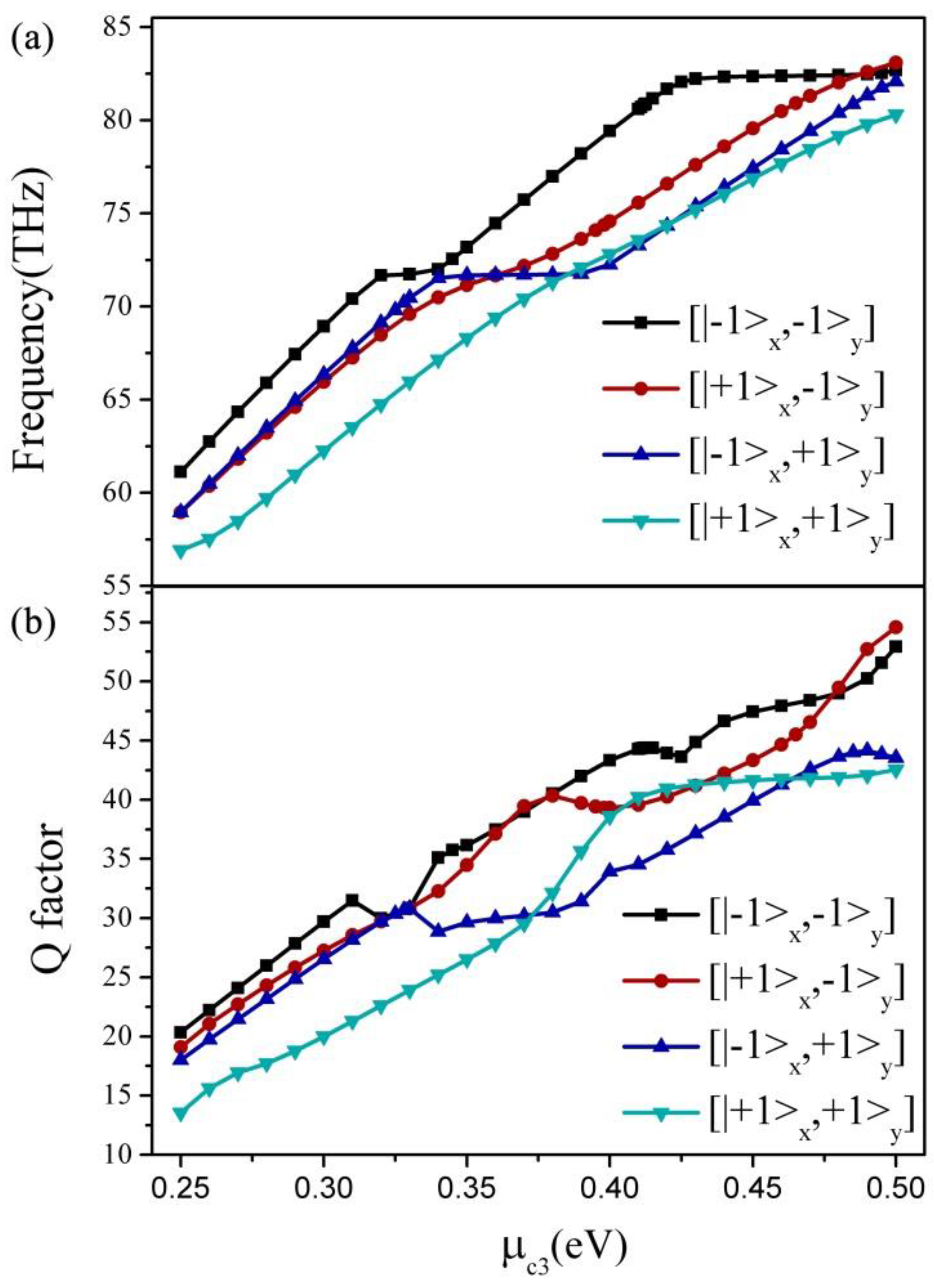
Then, we study the frequency and the Q factor of the plasmonic mode TM2,1 of the graphene plasmonic dimer as a function of the chemical potential of the nanodisk at the right side. Figure 6a,b plots the resonant frequency and the corresponding Q factor as a function of μc3 for the four mode categories. In the range from 0.25 to 0.5 eV, one can see that the frequencies of the two modes which are anti-symmetric with respect to the X direction, i.e., [|−1>x,|+1>y] and [|−1>x,|−1>y] modes, are similar. There is a notch in the Q factor of the [|−1>x,|−1>y] mode at μc3 = 0.33 eV, while there is a peak in the counterpart of the [|−1>x,|+1>y] mode at the same point. This is a typical avoid-crossing point [11,14]. However, unlike the photonic dimer composed of the coupled dielectric micro-disks, the Q factors of the [|−1>x,|+1>y] and [|−1>x,|−1>y] modes demonstrate a general climbing trend as the μc3 increases. This is due to the fact that the mismatching between the plasmons inside and outside the nanodisks becomes stronger when μc3 becomes higher, which also prevents the plasmons from escaping from the nanodisk and eventually results in a general increasing of the Q factor. In order to analyze the avoid-crossing property, we study the EM mode evolution as a function of μc3 and the corresponding diagrams are shown in Figure 7. For the [|−1>x,|−1>y] mode, when μc3 reduces from 0.5 to 0.425 eV, the resonant frequency remains stable at a platform of 82.5 THz. Also, the EM field of the left nanodisk does not change significantly and remains in the TM2,1 mode. However, the EM field of the right nanodisk is first weakened, then is enhanced again and switched from the TM2,1 mode to the TM3,1 mode. When μc3 reduces from 0.425 to 0.34 eV, the EM field in the right disk remains stable in the TM3,1 mode. However, the counterpart in the left disk is first weakened then is enhanced again. Also, it switches from the TM2,1 mode to the TM1,1 mode, and the resonant frequency reduces linearly from 83 to 72 THz with μc3. When μc3 further decreases from 0.34 to 0.325 eV, another resonant frequency platform appears at 72 THz. The EM mode of the left disk remains in the TM1,1 mode, and the field in the right disk is first weakened then enhanced again; the corresponding mode switches from TM3,1 to TM1,2. When μc3 further reduces to less than 0.325 eV, the plasmonic field in the right disk remains in the TM2,1 mode, but the field in the left disk disappears. Meanwhile, the resonant frequency decreases linearly with the reduction of μc3. As for the [|−1>x,|+1>y] mode, when μc3 reduces from 0.5 to 0.4 eV, the plasmonic mode in the right disk remains stable in the TM2,1 mode, while the mode in the left disk is first weakened and then enhanced. Also, the plasmonic mode switches from the TM2,1 mode to the TM1,1 mode in the left disk. At the same time, the resonant frequency decreases linearly from 83 THz to 71 THz with the reduction of μc3. Similar to the behavior of the [|−1>x,|+1>y] mode, a resonant frequency platform appears at around 71 THz when μc3 decreases from 0.4 to 0.33 eV. In this region, the plasmonic mode of the left disk remains stable in the TM1,1 mode, and the mode of the right disk is weakened first and then enhanced; also, the TM2,1 mode is switched to the TM3,1 mode. When μc3 further reduces to less than 0.325 eV, the mode field in the left disk weakens gradually and then eventually disappears. However, the right disk remains in the TM3,1 mode. Meanwhile, the resonant frequency decreases with the reduction of μc3. It should be noted that the bonding/anti-bonding state of the dimmer may be changed during the mode evolution procedure [35].
As for the modes which are symmetric with respect to the X axis, [|+1>x,|+1>y] and [|+1>x,|−1>y], there is also an avoid-crossing point at around 0.4 eV, which is shown in Figure 6. However, it is not as obvious as that of the asymmetric cases. This may be due to the large frequency splitting, which prevents the strong coupling effect between these two modes.
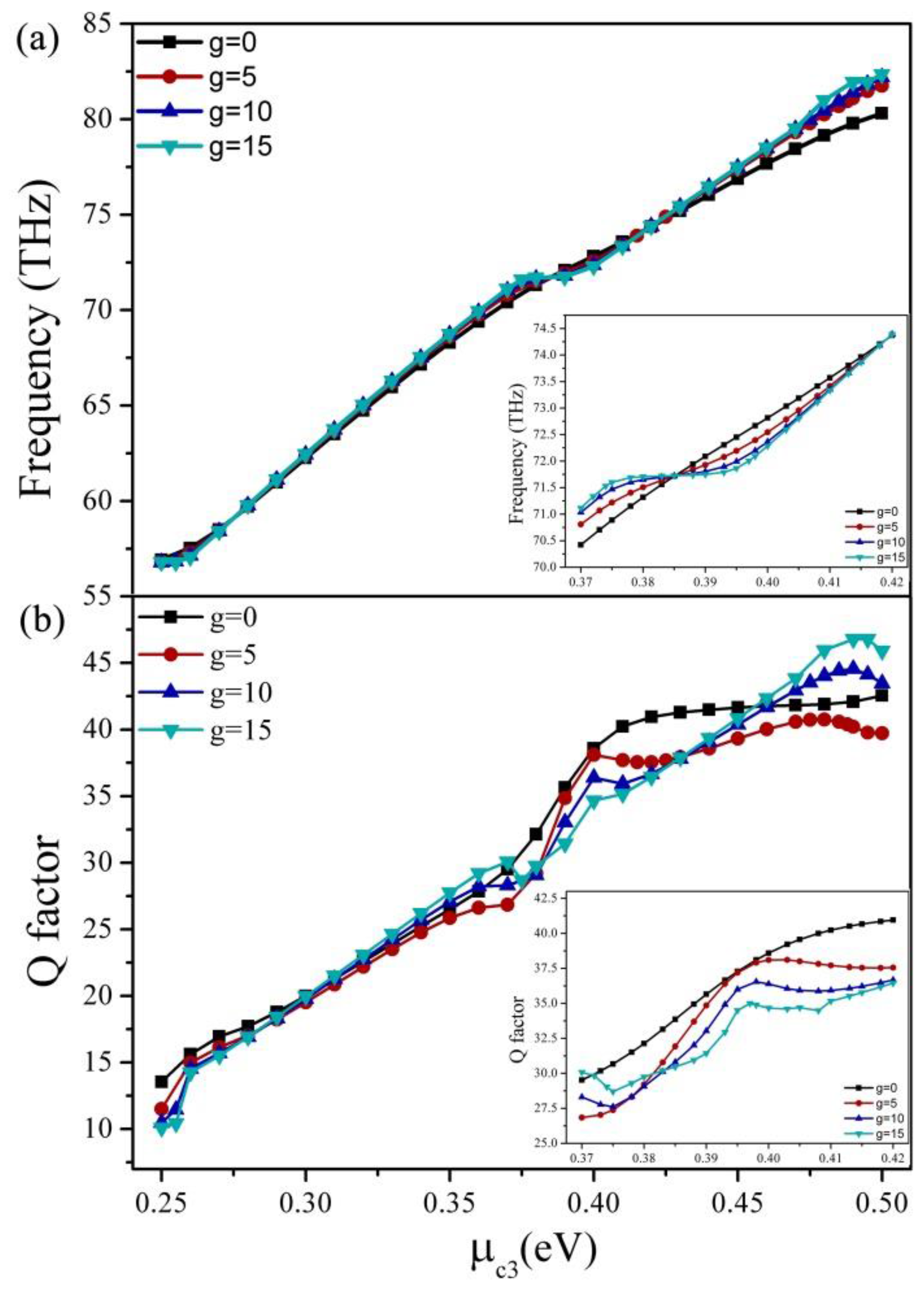
Figure 8 plots the resonance frequency of the [|+1>x,|+1>y] mode as a function of μc3 in a range from 0.25 to 0.5 eV with a gap distance from 0 to 15 nm. The insets show the details in a range between 0.37 and 0.42 eV. Interestingly, with the increasing of the gap distance, the “platform” effect on the resonance frequency becomes more significant, accompanied by the red-shift of the peak position of the Q factor. When the chemical potential μc3 decreases and passes the avoid-crossing point, i.e., 0.4 eV, the EM fields of the two nanodisks react with each other and result in the resonant frequency splitting, which is indicated in Figure 8a, accompanied by the appearance of the “platform” effect, peak of the Q factor, and the switching of the EM field distribution. Nevertheless, when the distance gap g reduces, the coupling becomes stronger, and the “platform” effect becomes weaker, which means that it is not necessary to “accumulate” the frequency reduction to ensure the EM field distribution switching. Also, the peak position of the Q factor shows a blue-shift as shown in Figure 8b.
4. Conclusions
In this paper, we proposed and numerically analyzed the EM properties of a plasmonic dimer composed of coupled graphene nanodisks. The resonant frequency and the corresponding Q factor of the anti-bonding mode increase as the distance gap increases between the nanodisks, while the opposite trend is observed in the case of the bonding mode. The frequency difference of both the anti-bonding modes and the bonding modes of the TMm,1 reduces as the azimuthal number m increases. An avoid-crossing property has been found in the anti-bonding modes when the chemical potential of the right disk μc3 decreased from 0.5 to 0.25 eV. In the future, more profound graphene nanoclusters will be constructed by adding more nanodisks for the investigation of dynamically tunable Fano resonance lineshape [36] and high order Fano resonance [37], where the graphene nanostructures interact with the external incident EM sources. Another graphene monolayer would be introduced underneath the graphene nanostructures separate ed by a dielectric spacer [38,39,40]. The proposed structure might offer a broad range of applications in both scientific and engineering fields such as light–matter interaction, tunable optical filters, and optical sensors.
Acknowledgments
The authors are grateful to the support by the Natural Science Fund of China under grant No. 61378058, the Science and Technology Fund of Quanzhou under grant No. Z1424009, Fujian Province Science Fund for Distinguished Young Scholars (No. 2015J06015) and the Promotion Program for Young and Middle-Aged Teachers in Science and Technology Research of Huaqiao University (No. ZQN-YX203).
Author Contributions
Weibin Qiu provided the original idea; Houbo Chen designed the models; Houbo Chen, Pingping Qiu, and Junbo Ren performed the simulations; Zhili Lin, Houbo Chen, Pingping Qiu, Junbo Ren, Jia-Xian Wang, Qiang Kan and Jiao-Qing Pan analyzed the data; Houbo Chen and Weibin Qiu wrote the paper.
Conflicts of Interest
The authors declare no conflict of interest.
References
- Chuntonov, L.; Haran, G. Trimeric plasmonic molecules: The role of symmetry. Nano Lett. 2011, 11, 2440–2445. [Google Scholar] [CrossRef] [PubMed]
- Chuntonov, L.; Haran, G. Effect of Symmetry Breaking on the Mode Structure of Trimeric Plasmonic Molecules. J. Phys. Chem. C 2011, 115, 19488–19495. [Google Scholar] [CrossRef]
- Fan, J.A.; Bao, K.; Wu, C.; Bao, J.; Bardhan, R.; Halas, N.J.; Manoharan, V.N.; Shvets, G.; Nordlander, P.; Capasso, F. Fano-like interference in Self-Assembled plasmonic quadrumer clusters. Nano Lett. 2010, 10, 4680–4685. [Google Scholar] [CrossRef] [PubMed]
- Hentschel, M.; Saliba, M.; Vogelgesang, R.; Giesse, H.; Alivisatos, A.P.; Liu, N. Transition from Isolated to Collective Modes in Plasmonic Oligomers. Nano Lett. 2010, 10, 2721–2726. [Google Scholar] [CrossRef] [PubMed]
- Luk’Yanchuk, B.; Zheludev, N.I.; Maier, S.A.; Hals, N.J.; Nordlander, P.; Giessen, H.; Chong, C.T. The Fano resonance in plasmonic nanostructures and metamaterials. Nat. Mater. 2010, 9, 707–715. [Google Scholar] [CrossRef] [PubMed]
- Feng, S.; Gan, L. Multi-channel slow light coupled-resonant waveguides based on photonic crystal with rectangular microcavities. Opt. Commun. 2015, 341, 257–262. [Google Scholar] [CrossRef]
- Papasimakis, N.; Fedotov, V.A.; Zheludev, N.I.; Prosvirnin, S.L. Metamaterial analog of electromagnetically induced transparency. Phys. Rev. Lett. 2008, 101, 253903. [Google Scholar] [CrossRef] [PubMed]
- Liu, N.; Langguth, L.; Weiss, T.; Kastel, J.; Fleischhauer, M.; Pfau, T.; Giessen, H. Plasmonic analogue of electromagnetically induced transparency at the Drude damping limit. Nat. Mater. 2009, 8, 758–762. [Google Scholar] [CrossRef] [PubMed]
- Liu, N.; Weiss, T.; Mesch, M.; Langguth, L.; Eigenthaler, U.; Hirscher, M.; Sonnichsen, C.; Giessen, H. Planar metamaterial analogue of electromagnetically induced transparency for plasmonic sensing. Nano Lett. 2010, 10, 1103–1107. [Google Scholar] [CrossRef] [PubMed]
- Mukherjee, S.; Sobhani, H.; Lassiter, J.B.; Bardhan, R.; Nordlander, P.; Halas, N.J. Fanoshells: Nanoparticles with built-in fano resonances. Nano Lett. 2010, 10, 2694–2701. [Google Scholar] [CrossRef] [PubMed]
- Ozbay, E.; Bayindir, M.; Bulu, I.; Cubukcu, E. Investigation of localized Coupled-Cavity modes in Two-Dimensional photonic bandgap structures. IEEE J. Quantum Elect. 2002, 38, 837–843. [Google Scholar] [CrossRef]
- Wang, Q.; Zhao, H.; Du, X.; Zhang, W.; Qiu, M.; Li, Q. Hybrid photonic-plasmonic molecule based on metal/Si disks. Opt. Express 2013, 21, 11037–11047. [Google Scholar] [CrossRef] [PubMed]
- Ryu, J.; Lee, S.; Kim, S.W. Coupled nonidentical microdisks: Avoided crossing of energy levels and unidirectional far-field emission. Phys. Rev. A 2009, 79, 53858. [Google Scholar] [CrossRef]
- Boriskina, S.V. Coupling of whispering-gallery modes in size-mismatched microdisk photonic molecules. Opt. Lett. 2007, 32, 1557–1559. [Google Scholar] [CrossRef] [PubMed]
- Chen, P.; Alu, A. Atomically thin surface cloak using graphene monolayers. ACS Nano 2011, 5, 5855–5863. [Google Scholar] [CrossRef] [PubMed]
- Huang, Y.X.; Zhao, J.; Qiu, W.B.; Lin, S.X.; Chen, H.B.; Wang, J.X.; Kan, Q.; Pan, J.Q. Investigation of the tunable plasmonic whispering gallery mode properties for graphene monolayer nanodisk cavities. Optik 2016, 127, 5591–5596. [Google Scholar] [CrossRef]
- Zhao, J.; Qiu, W.B.; Huang, Y.X.; Wang, J.X.; Kan, Q.; Pan, J.Q. Investigation of plasmonic whispering-gallery mode characteristics for graphene. Opt. Lett. 2014, 39, 5527–5530. [Google Scholar] [CrossRef] [PubMed]
- Zhu, X.L.; Wang, W.L.; Yan, W.; Larsen, M.B.; Boggild, P.; Pedersen, T.G.; Xiao, S.S.; Zi, J.; Mortensen, A. Plasmon-phonon coupling in large-area graphene dot and antidot arrays fabricated by nanosphere lithograhey. Nano Lett. 2014, 14, 2907–2913. [Google Scholar] [CrossRef] [PubMed]
- Maes, B.; Rosolen, G. Asymmetric and connected graphene dimers for a tunable plasmonic response. Phys. Rev. B 2015, 92, 205405. [Google Scholar]
- Hadad, Y.; Steinberg, B.Z. Quasistatic resonance of a chemical potential interruption in a graphene layer and its polarizability: The mixed-polarity semilocalized plasmon. Phys. Rev. B 2013, 88, 075439. [Google Scholar] [CrossRef]
- Hadad, Y.; Davoyan, A.R.; Engheta, N.; Steinberg, B.Z. Extreme and Quantized Magneto-optics with Graphene Meta-atoms and Metasurfaces. ACS Photonics 2014, 1, 1068–1073. [Google Scholar] [CrossRef]
- Qiu, W.B.; Huang, Y.X.; Chen, H.B.; Qiu, P.P.; Tang, Y.X.; Wang, J.X.; Kan, Q.; Pan, J.Q. Coupling of Whispering-Gallery modes in the graphene nanodisk plasmonic dimers. Plasmonics 2016, 12, 1–7. [Google Scholar] [CrossRef]
- Huang, F.; Baumberg, J.J. Actively tuned plasmons on elastomerically driven Au nanoparticle dimers. Nano Lett. 2010, 10, 1787–1792. [Google Scholar] [CrossRef] [PubMed]
- Acimovic, S.S.; Kreuzer, M.P.; Gonzalez, M.U.; Quidant, R. Plasmon near-field coupling in metal dimers as a step toward single-molecule sensing. ACS Nano 2009, 3, 1231–1237. [Google Scholar] [CrossRef] [PubMed]
- Large, N.; Abb, M.; Aizpurua, J.; Muskens, O.L. Photoconductively loaded plasmonic nanoantenna as building block for ultracompact optical switches. Nano Lett. 2010, 10, 1741–1746. [Google Scholar] [CrossRef] [PubMed]
- Huang, Y.X.; Qiu, W.B.; Lin, S.X.; Chen, H.B.; Wang, J.X.; Kan, Q.; Pan, J.Q. Analysis of mode characteristics and output efficiency of graphene equilateral triangle nanocavity with vertex output waveguide. Opt. Quantum Electron. 2016, 48, 1–10. [Google Scholar] [CrossRef]
- Hanson, G.W. Dyadic Green’s functions and guided surface waves for a surface conductivity model of graphene. J. Appl. Phys. 2008, 103, 64302. [Google Scholar] [CrossRef]
- Qiu, W.B.; Liu, X.H.; Zhao, J.; He, S.H.; Ma, Y.H.; Wang, J.X.; Pan, J.Q. Nanofocusing of mid-infrared electromagnetic waves on graphene monolayer. Appl. Phys. Lett. 2014, 104, 41109. [Google Scholar] [CrossRef]
- Zhao, J.; Liu, X.H.; Qiu, W.B.; Ma, Y.H.; Huang, Y.X.; Wang, J.X.; Qiang, K.; Pan, J.Q. Surface-plasmon-polariton whispering-gallery mode analysis of the graphene monolayer coated InGaAs nanowire cavity. Opt. Express 2014, 22, 5754–5761. [Google Scholar] [CrossRef] [PubMed]
- Vakil, A.; Engheta, N. Transformation optics using graphene. Science 2011, 332, 1291–1294. [Google Scholar] [CrossRef] [PubMed]
- Efetov, D.K.; Kim, P. Controlling Electron-Phonon interactions in graphene at ultrahigh carrier densities. Phys. Rev. Lett. 2010, 105, 256805. [Google Scholar] [CrossRef] [PubMed]
- Low, T.; Avouris, P. Graphene plasmonics for terahertz to Mid-Infrared applications. ACS Nano 2014, 8, 1086–1101. [Google Scholar] [CrossRef] [PubMed]
- Huang, Y.X.; Qiu, W.B.; Lin, S.X.; Zhao, J.; Chen, H.B.; Wang, J.X.; Kan, Q.; Pan, J.Q. Investigation of plasmonic whispering gallery modes of graphene equilateral triangle nanocavities. Sci. China Inf. Sci. 2016, 59, 1–9. [Google Scholar] [CrossRef]
- Kwon, S.H. Deep subwavelength plasmonic whispering-gallery-mode cavity. Opt Express 2012, 20, 24918–24924. [Google Scholar] [CrossRef] [PubMed]
- Zhang, S.; Li, G.C.; Chen, Y.Q.; Zhu, X.P.; Liu, S.D.; Lei, D.Y.; Duan, H.G. Pronounced fano resonance in single gold split nanodisks with 15 nm split gaps for intensive second harmonic generation. ACS Nano 2016, 10, 11105–11114. [Google Scholar] [CrossRef] [PubMed]
- Rahmani, M.; Lei, D.Y.; Giannini, V.; Lukiyanchuk, B.; Ranjbar, M.; Liew, T.Y.F.; Hong, M.H.; Maier, S.A. Subgroup decomposition of plasmonic resonances in hybrid oligomers: Modeling the resonance lineshape. Nano Lett. 2012, 12, 2101–2106. [Google Scholar] [CrossRef] [PubMed]
- Liu, S.D.; Leong, E.S.P.; Li, G.C.; Deng, J.; Teng, J.H.; Ong, H.C.; Lei, D.Y. Polarization-independent multiple fano resonances in plasmonic nonamers for multimode-matching enhanced multiband second-harmonic generation. ACS Nano 2016, 10, 1442–1453. [Google Scholar] [CrossRef] [PubMed]
- Lei, D.Y.; Fernandez-Dominguez, A.I.; Sonnefraud, Y.; Appavoo, K.; Haglundjr, R.F.; Pendry, J.B.; Maier, S.A. Revealing plasmonic gap modes in particle-on-film systems using dark-field spectroscopy. ACS Nano 2012, 6, 1380–1386. [Google Scholar] [CrossRef] [PubMed]
- Li, G.C.; Zhang, Y.L.; Lei, D.Y. Hybrid plasmonic gap modes in metal film-coupled dimers and their physical origins revealed by polarization resolved dark field spectroscopy. Nanoscale 2016, 8, 7119–7126. [Google Scholar] [CrossRef] [PubMed]
- Li, G.C.; Zhang, Y.L.; Jiang, J.; Luo, Y.; Lei, D.Y. Metal-substrate-mediated plasmon hybridization in a nanoparticle dimer for photoluminescence line-width shrinking and intensity enhancement. ACS Nano 2017. [Google Scholar] [CrossRef] [PubMed]
Figure 1.
The 2D schematic of the graphene nanodisk dimer molecule, where R is the radius of the nanodisk; μc2 and μc3 are the chemical potentials of each nanodisk.
Figure 1.
The 2D schematic of the graphene nanodisk dimer molecule, where R is the radius of the nanodisk; μc2 and μc3 are the chemical potentials of each nanodisk.
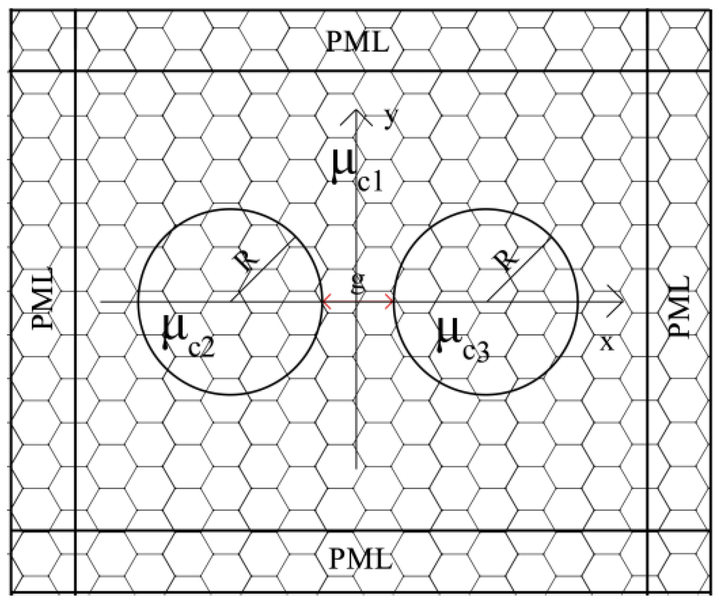
Figure 2.
The electric field z component distribution of the collective mode TM2,1. (a) g = 0 nm and (b) g = 15 nm.
Figure 2.
The electric field z component distribution of the collective mode TM2,1. (a) g = 0 nm and (b) g = 15 nm.

Figure 3.
(a) Frequency and (b) Q factor of the collective modes TM2,1 as a function of g of the four categories of symmetry, where μc2 = μc3 = 0.5 eV, μc1 = 0.1 eV and R = 50 nm.
Figure 3.
(a) Frequency and (b) Q factor of the collective modes TM2,1 as a function of g of the four categories of symmetry, where μc2 = μc3 = 0.5 eV, μc1 = 0.1 eV and R = 50 nm.
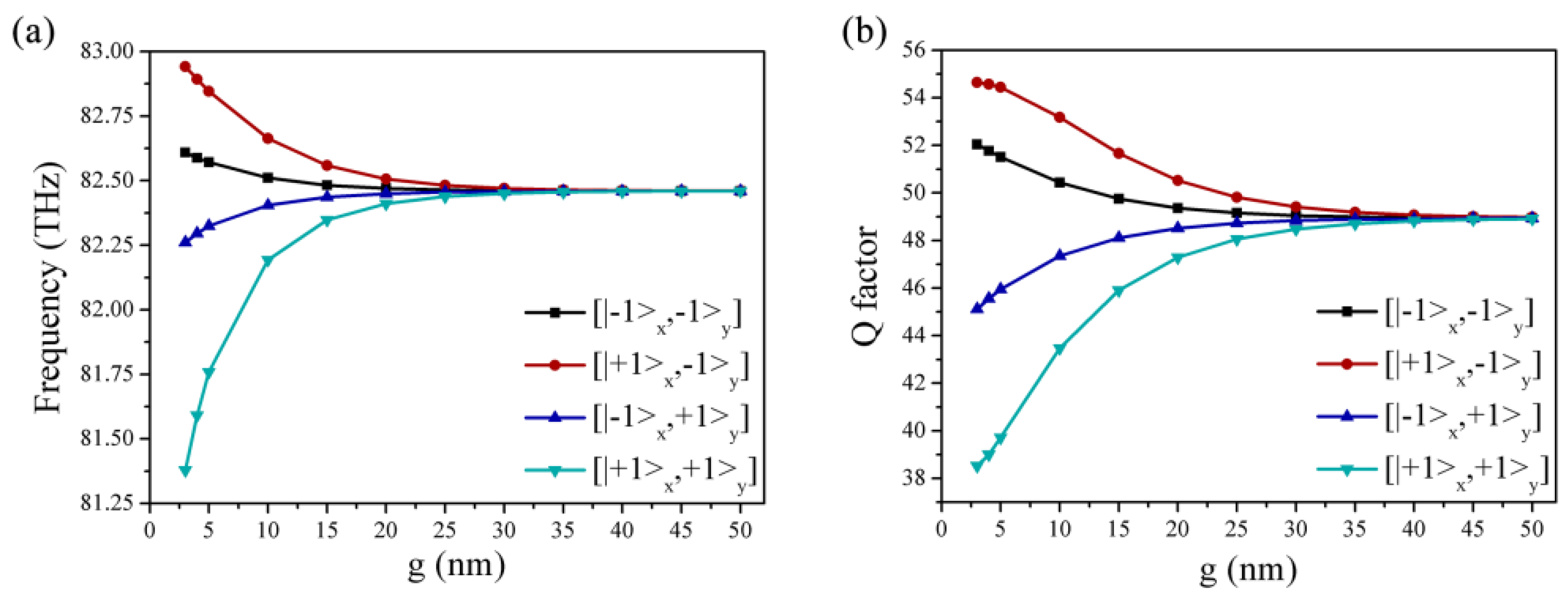
Figure 4.
The real part and the absolute value of the imaginary part of the propagation constant as a function of frequency, where the chemical potential of the grapheme is 0.5 eV, respectively.
Figure 4.
The real part and the absolute value of the imaginary part of the propagation constant as a function of frequency, where the chemical potential of the grapheme is 0.5 eV, respectively.
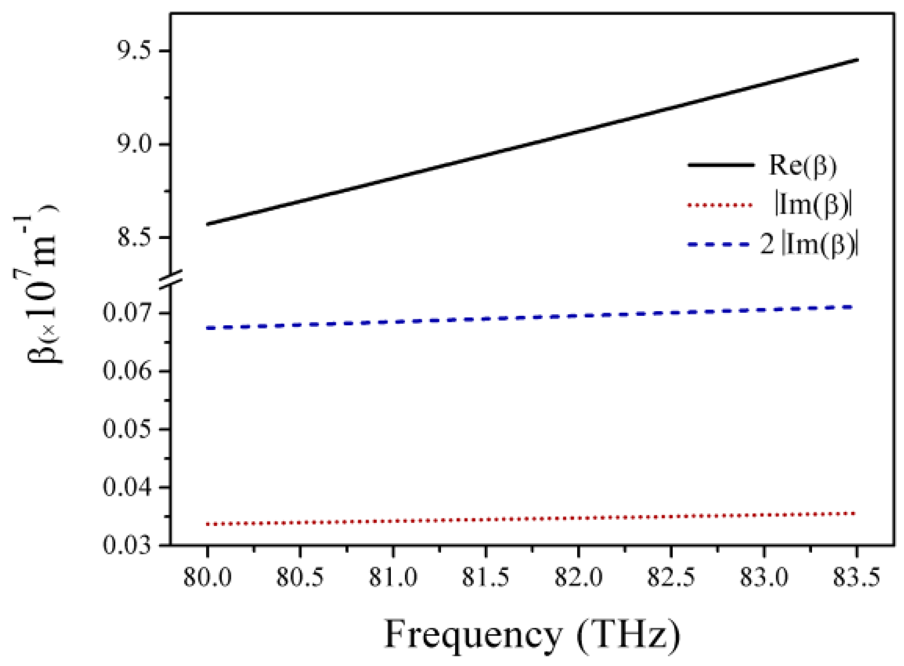
Figure 5.
The frequency splitting ΔF of bonding and anti-bonding whispering-gallery (WG) modes of TMm,1 as a function of m from 2 to 8, where the distance g is 5 nm.
Figure 5.
The frequency splitting ΔF of bonding and anti-bonding whispering-gallery (WG) modes of TMm,1 as a function of m from 2 to 8, where the distance g is 5 nm.
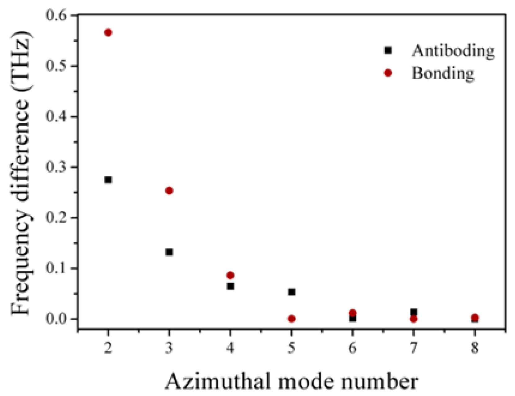
Figure 6.
The variation of the frequency and Q factor of the fundamental mode as a function of the chemical potential μc3. (a) Resonance frequency; (b) Q factor.
Figure 6.
The variation of the frequency and Q factor of the fundamental mode as a function of the chemical potential μc3. (a) Resonance frequency; (b) Q factor.

Figure 7.
The frequencies of [|−1>x,|−1>y] and [|−1>x,|+1>y] modes as a function of the chemical potential μc3.
Figure 7.
The frequencies of [|−1>x,|−1>y] and [|−1>x,|+1>y] modes as a function of the chemical potential μc3.
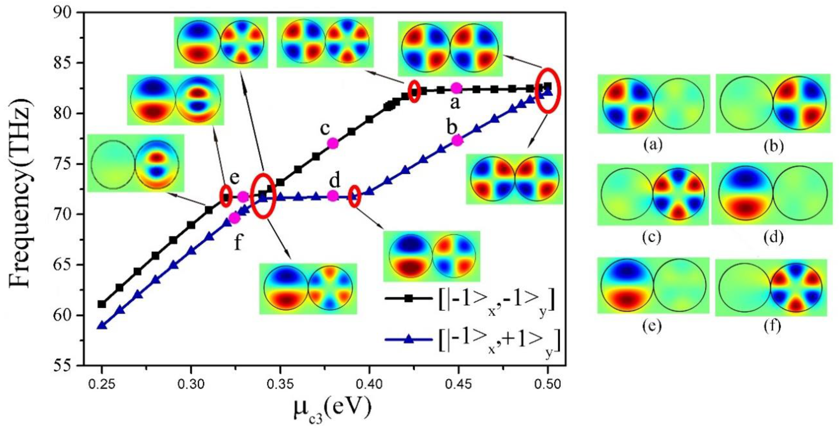
Figure 8.
The resonant frequency and the corresponding Q factor as a function of chemical potential μc3 with various gap distances. The insets show the details with a chemical potential from 0.39 to 0.41 eV. (a) Resonance frequency; (b) Q factor.
Figure 8.
The resonant frequency and the corresponding Q factor as a function of chemical potential μc3 with various gap distances. The insets show the details with a chemical potential from 0.39 to 0.41 eV. (a) Resonance frequency; (b) Q factor.
© 2017 by the authors. Licensee MDPI, Basel, Switzerland. This article is an open access article distributed under the terms and conditions of the Creative Commons Attribution (CC BY) license (http://creativecommons.org/licenses/by/4.0/).
Share and Cite
MDPI and ACS Style
Chen, H.; Qiu, W.; Qiu, P.; Ren, J.; Lin, Z.; Wang, J.-X.; Kan, Q.; Pan, J.-Q. Mode Coupling Properties of the Plasmonic Dimers Composed of Graphene Nanodisks. Appl. Sci. 2017, 7, 359. https://doi.org/10.3390/app7040359
AMA Style
Chen H, Qiu W, Qiu P, Ren J, Lin Z, Wang J-X, Kan Q, Pan J-Q. Mode Coupling Properties of the Plasmonic Dimers Composed of Graphene Nanodisks. Applied Sciences. 2017; 7(4):359. https://doi.org/10.3390/app7040359
Chicago/Turabian StyleChen, Houbo, Weibin Qiu, Pingping Qiu, Junbo Ren, Zhili Lin, Jia-Xian Wang, Qiang Kan, and Jiao-Qing Pan. 2017. "Mode Coupling Properties of the Plasmonic Dimers Composed of Graphene Nanodisks" Applied Sciences 7, no. 4: 359. https://doi.org/10.3390/app7040359
Note that from the first issue of 2016, this journal uses article numbers instead of page numbers. See further details here.