Article

Solar Explosive Evaporation Growth of ZnO Nanostructures

1
I. Frantsevich Institute for Problems of Material Science, National Academy of Science of Ukraine, 3 Krzhizhanovskogo Street, 03680 Kyiv, Ukraine
2
V. Bakul Institute for Superhard Materials, National Academy of Science of Ukraine, 2 Avtozavodskaya str., 04074 Kyiv, Ukraine
3
V. Lashkarev Institute of Semiconductor Physic, National Academy of Science of Ukraine, 45 Nauky pr., 03028 Kyiv, Ukraine
4
Department of Physics, Chemistry and Biology (IFM), Linköping University, 581 83 Linköping, Sweden
*
Author to whom correspondence should be addressed.
Appl. Sci. 2017, 7(4), 383; https://doi.org/10.3390/app7040383
Submission received: 10 November 2016 / Revised: 9 February 2017 / Accepted: 21 February 2017 / Published: 12 April 2017
(This article belongs to the Special Issue Metal Oxide Nanostructures)

Abstract

:
For the first time, we present a novel method of explosive evaporation (MEE) for the deposition of ZnO nanostructures using concentrated solar radiation for precursor evaporation. Zinc acetylacetonate powder and a mixture of ZnO with graphite powders are used as precursors for the deposition of ZnO nanostructures. ZnO nanostructures are deposited on Au/Si, Ag/Si, and unpolished Si substrates by MEE. The scanning electron microscopy, energy dispersive X-ray analysis, X-ray diffraction, Raman scattering, photoluminescence, and Fourier transformed infrared spectroscopy are used for sample characterization. We demonstrate that the changing of precursors and the substrate types allows ZnO nanostructures to be grown with diverse morphologies: hexagons, spheres, and needles. The properties of ZnO nanostructures deposited on unpolished, coated by Ag and Au silicon substrates are discussed. MME using concentrated solar radiation is promising method for applications in the semiconductor industry as an economically efficient environmentally-friendly method for the growth of nanostructures.

Graphical Abstract

1. Introduction

Zinc oxide (ZnO) micro- and nanostructures are of considerable scientific interest due to the prospect of their applications for the development of chemical sensors with increased specific surface area, sources of ultraviolet and light emitting diodes, solar cells, electron-field display systems, etc. [1,2]. Metal–organic chemical vapour deposition (MOCVD), vapour phase epitaxy (VPE), pulsed laser deposition (PLD), direct carbo-thermal evaporation, aqueous chemical growth (ACG), and electrochemical deposition are growth techniques which are widely used for the deposition of ZnO nanostructures [3,4]. Zinc acetylacetonate [5] and/or mixtures of ZnO + C powder [1] are used as precursors for the growth of ZnO nanostructures in such deposition methods as MOCVD, vapour phase epitaxy, and direct carbo-thermal evaporation. Traditionally, these precursors evaporated by different electrical heaters or the last ones were placed in a furnace using quartz tubes as synthesis reactors that result in low-speed evaporation of precursors. The inertia of such heaters may lead to problems with the uniformity and stoichiometric ratio of ZnO nanostructures [5,6,7,8]. Therefore, the development of growth methods with high-speed precursor evaporation is interesting for the deposition of uniformly high-quality ZnO nanostructures. On the other hand, the depletion of fossil fuels has led to a great interest in renewable energy resources. Taking all this into consideration, we propose a method of ZnO nanostructures growth that makes use of a solar concentrator. In a solar concentrator, the energy of the Sun is focused on the place where precursor boat is arranged. So, the use of concentrated solar radiation allows the implementation of the condition for high-speed evaporation of the precursor. Firstly, we called the proposed method of deposition the method of explosive evaporation (MEE) because a precursor evaporated very quickly (resembling an explosion) due to the application of high power concentrated solar radiation. Furthermore, compared to traditional methods, the proposed MEE has the advantage of additional activation of ad-atoms by the ultraviolet (UV) part of solar radiation that is important for the deposition of high crystal perfection ZnO nanostructures. In PLD method for ZnO growth, the effect of ad-atoms activation is realized by UV eximer laser.
It is shown in [3,6] that the application of substrates covered by catalysts (Au or Ag) influences the morphologies of ZnO nanostructures. Moreover, the application of the unpolished substrates may be interesting for the deposition of nanostructures because the surface has its own nucleation centers. Hence, we report the study of the properties for ZnO nanostructures deposited at high-speed growth conditions the by method of explosive evaporation on unpolished Si, Au/Si, and Ag/Si substrates.

2. Materials and Methods

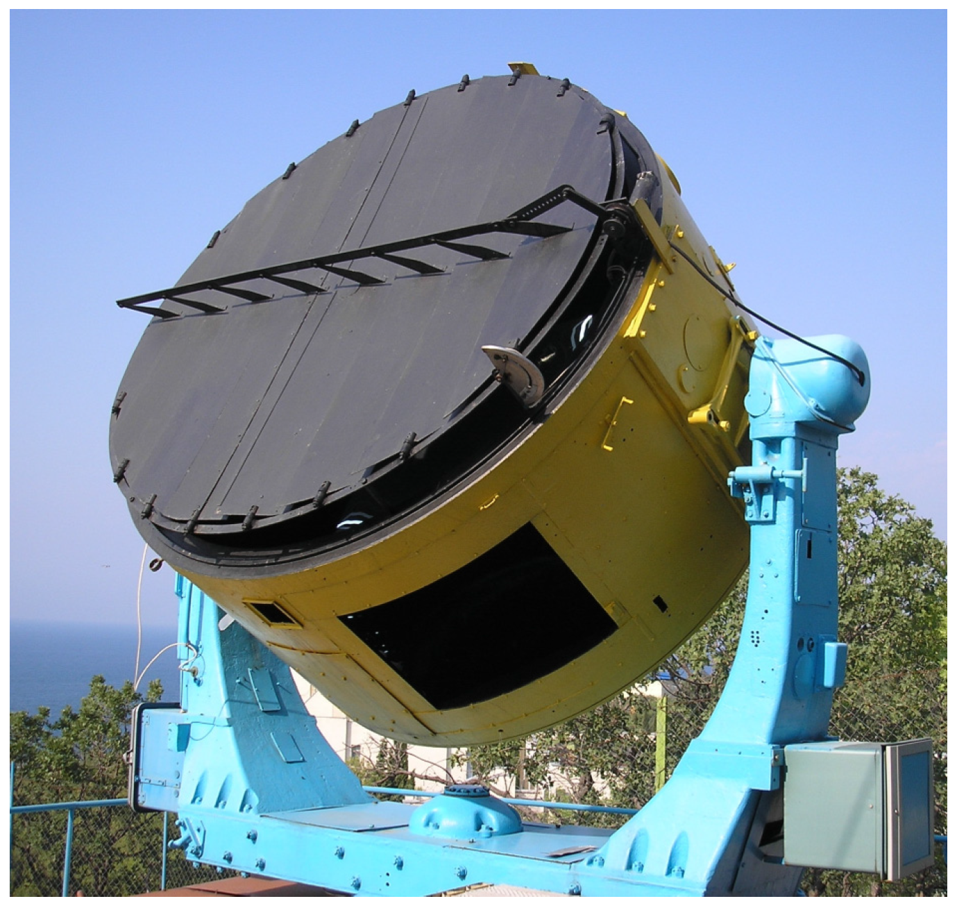
2.1. Samples Preparation

ZnO nanostructures were grown on unpolished Si substrates and on polished Si substrates coated by Au and Ag films by MEE using concentrated solar radiation. A 60 nm thick layer of Au film and a 200 nm thick layer of Ag film were deposited on the substrate by radio frequency (RF) magnetron sputtering and thermal evaporation, respectively. Au/Si, Ag/Si, and unpolished Si substrates had the size of 5 × 5 mm2. Before loading substrates into the quartz tube, the last ones were cleaned successively in acetone, ethanol, and deionised water for 10 min for each stage. After that, the substrates were dried in nitrogen flow.
The growth of ZnO nanostructures was carried out using the solar concentrator of the Geliocenter of the Institute for Problems of Materials Science (Crimea, Ukraine). The solar concentrator based on a converted army floodlight (see Figure 1) is equipped with an automatic sun tracking system and a mounting mechanism for fixing the quartz tube. The mounting mechanism is placed inside the solar concentrator and allows to fix the sealed-on-one-side quartz tube with 10 mm diameter in the focus of a 2-m diameter mirror. The other end of the tube remained open for free access of air. In the middle of the tube was placed the boat filled with precursors of the powder of zinc acetylacetonate hydrate (Zn(AcAc)2:Zn(C2H7O5)2-H2O) or a mixture of ZnO and graphite powders (with 1:1 mole ratio) with weight of about 1 g. All precursors were from Sigma Aldrich (Saint Louis, MS, USA) with purity no less than 99% [8]. Changing the angle of the louver (please see Figure 1) of the solar concentrator allows the heating temperature in focus to be set up to 3000 °C. The angle of opening for the louver was changed in the range of 15°–30° for adjustment of temperature for precursor evaporation in range from 300 to 900 °C. The temperature of evaporation was controlled by platinum–rhodium thermocouple. The temperatures of 300 °C and of 900 °C were used for the evaporation of precursors of zinc acetylacetonate and of a mixture of ZnO and graphite powders, respectively. Au/Si and Ag/Si substrates together were used in experiment when zinc acetylacetonate was decomposed for obtaining ZnO. The carbothermal reduction of mixtures of ZnO + C powders we used at the deposition of ZnO nanostructures on unpolished Si substrates. In all cases, the substrates were placed at a distance of 20 mm from the heating zone, and the deposition time was about 3 min.

2.2. Characterization
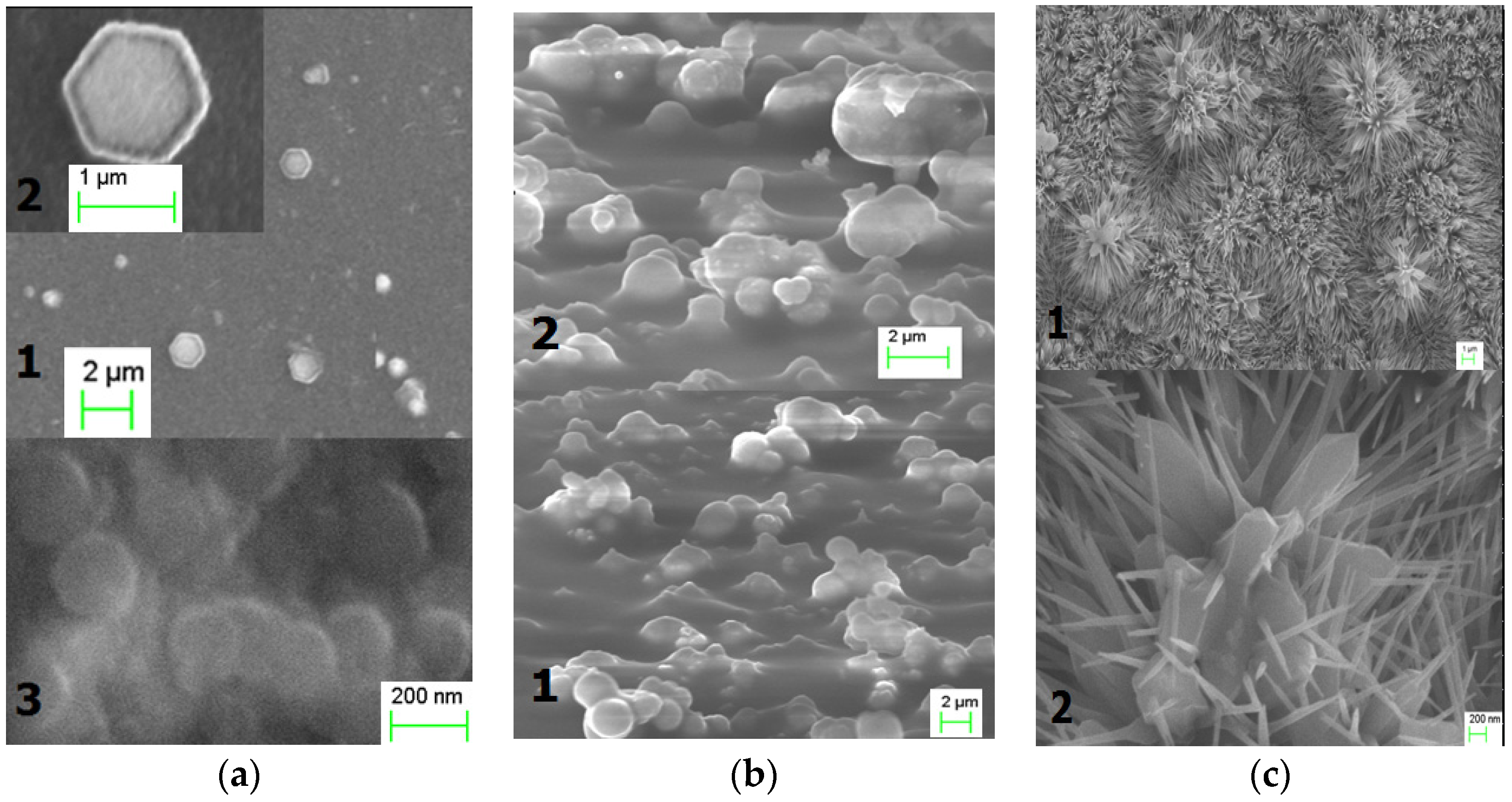
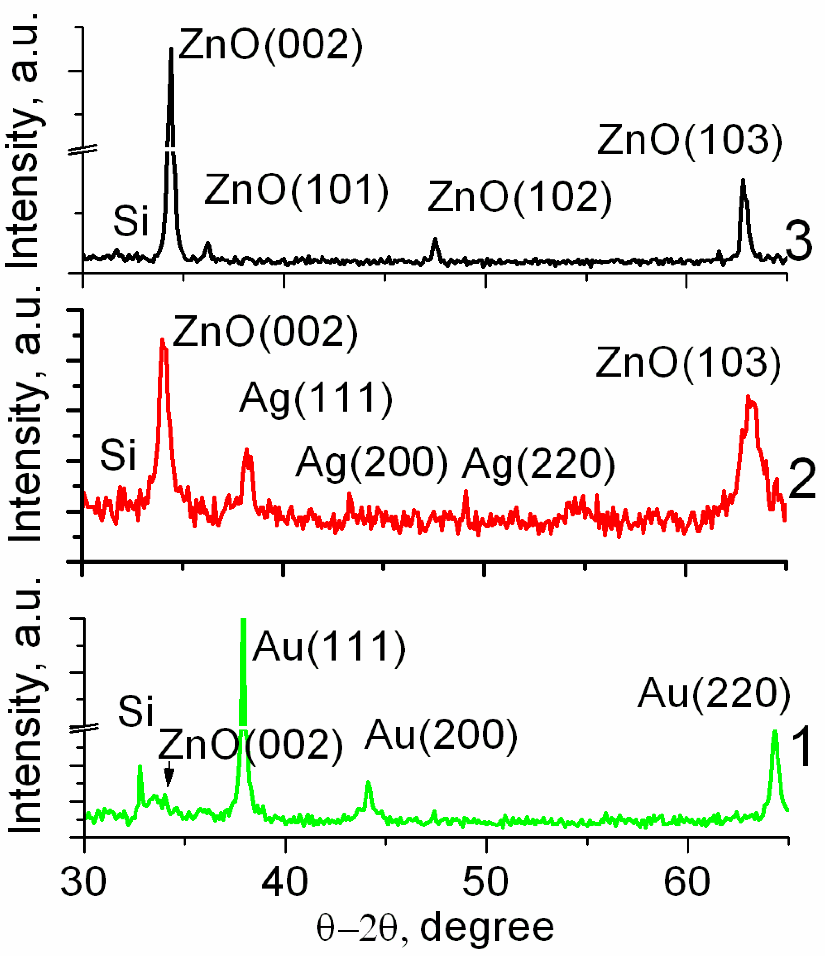
The crystal structure of ZnO nanostructures was investigated by X-ray diffraction (XRD) using DRON-4 diffractometer, utilizing Cu-Kα radiation (λ = 0.1542 nm). A MII-4 interferometer was used to estimate the thickness of Ag and Au films deposited on Si substrates. The microstructure was studied by scanning electron microscopy (SEM) using a ZEISS EVO 50 XVP. The elemental analysis was also done by ZEISS EVO 50 XVP SEM (Carl Zeiss AG, Oberkochen, Germany) using energy dispersive X-ray spectroscopy (EDX) furnished INCA 450 (OXFORD Instruments, Oxford ,UK). The software of SEM and EDX equipment was used to estimate the heights of the nanostructures [9]. Photoluminescence (PL) measurement was performed at room temperature by optical excitation using a Nd:YVO laser (266 nm). The micro-Raman measurements were carried out in backscattering geometry at room temperature using a Horiba Jobin Yvon T64000 system equipped with an Olympus confocal optical microscope. Fourier transform infrared spectrometry (FTIR) was carried out on an IR microscope Nicolet 6700 equipped with a motorized objective table.

3. Results

SEM images of ZnO nanostructures deposited on different substrates by MEE using concentrated solar radiation for precursor decomposition are present in Figure 2. As can be seen from Figure 2a (region 1), ZnO hexagons grown on Au/Si substrates have two different geometric sizes. The large ones (area 2 on Figure 2a) that were heterogeneously grown on the Au/Si substrate have diameters of about 1200–1300 nm. Having diameters about of 200–220 nm, the small hexagons (area 3 on Figure 2a) uniformly covered the Au/Si substrate. The estimated height of the large hexagons was about 40 nm, and the height of small hexagons was about 6 nm, as determined by the use of the SEM and EDX equipment software. At similar deposition conditions, nanostructures in the form of the spheres (region 1 on Figure 2b) and in the form of “mushrooms” (see region 2 on Figure 2b) were grown on Ag/Si substrates. The deposited structures had sizes of about 500–2500 nm. EDX measurements confirmed that the whole Ag/Si substrates were covered by ZnO, having a spherical morphology in some regions. Therefore, the application of zinc acetylacetonate precursor led to the growth of hexagons on Au/Si substrates opposite to the growth of the spheres on Ag/Si substrates.
The deposition of nanostructures by MEE using the carbothermal reduction for ZnO growth led to growth of the nanoneedles on unpolished Si substrates in the shape of “hedgehogs in the grass” (see region 1 on Figure 2c). The grown structures had crystal-like basis with diameters about 200–250 nm which ended with a needle of diameter ~40 nm (region 2 on Figure 2c). EDX examinations of the needles determined that latter consist of ZnO.
The analysis of EDX results allowed us to determine that all grown nanostructures were ZnO (see Supplementary Materials Figure S1a–c). The presence of carbon in large amounts was found on the surface of ZnO hexagons and ZnO spheres (Figure S1a,b). However, the surface of the ZnO nanoneedles contained the least amount of carbon (Figure S1c). Therefore, the application of mixture of ZnO with graphite powders precursor was more favorable than the zinc acetylacetonate precursor. Additional investigation of the influence of the technological parameters (e.g., boat–substrates distance) on the degree of carbon contamination is required.
XRD patterns presented in Figure 3 confirm EDX data: all deposited nanostructures have wurtzitic structure of ZnO. Additionally, the reflection peaks of Au(111), Au(200), Au(220), as well as those of Ag(111), Ag(200), and Ag(220) are shown in the XRD patterns. No other diffraction peaks are shown in Figure 3.
The parameters of XRD peaks, approximated by Gaussian function, are presented in Table 1. Each type of ZnO nanostructure has its own set of crystallographic planes: hexagons—(002), spheres—(002), (103), (112), and needles—(002), (101), (102), (103) (JCPDS card number 36–1451). The small magnitude of the full width at half maximum (FWHM) of diffraction peak ZnO (002) of 0.12–0.18 degrees (Table 1) results in high magnitude of grain size as estimated by Scherrer’s formula [10] about 45–50 nm for the hexagons and the needles, respectively. This confirms their high crystalline quality. It should be also noted that the hexagons and the needles have similar crystal-like nature: the hexagons are oriented perpendicular to plane of the substrates, while the needles are hexagon-like crystals that are ended by needles oriented at different angles to the substrate due to heterogeneity of the surface of unpolished Si substrates. In the case of the spheres, XRD peaks of (002), (103), (112) have similar integral intensities. This may be due to their sphere-like morphology. ZnO nanoneedles demonstrated the largest integral intensity of XRD peaks, suggesting their crystalline quality was best among the others.
FTIR spectroscopy was used for investigation of the aforementioned ZnO nanostructures. Generally, it is possible to study the chemisorbed contamination in nanostructures as well as the distribution of the latest ones over the substrate surface. Figure 4 shows typical reflectance spectra for ZnO nanostructures deposited on Au/Si (curve 1), Ag/Si (curve 2), and unpolished Si (curve 3) substrates. It was not possible to investigate samples in transmittance mode, because Au/Si, Ag/Si, and Si substrates were not transparent. FTIR measurements of the given spectral range will not allow us to establish the fact of the formation of ZnO, because the Zn-O vibration bond at 482 cm−1 [11] is located outside of the spectral range of the measurements. The typical reflectance spectra of ZnO nanostructures reveal the absence of good resolved peaks associated with chemisorbed contaminations on the surface of ZnO nanostructures (Figure 4).
It is significant to note that Raman scattering studies are very sensitive for determining crystal perfection and structural defects. Figure 5 presents ZnO Raman spectrum only for ZnO nanoneedles due to their homogeneous dense bulk arrangement on the surface of Si substrate and due to the confocal nature of Raman scattering measurements. Raman signals were unable to be obtained for uniformly grown ZnO hexagons and ZnO spheres that have small bulks and because of the presence of carbon on the surfaces of nanostructures (Figure S1a,b). In the Raman spectra of ZnO nanoneedles (Figure 5), there is a well-known intense E2low phonon band at 98.9 cm−1 (FWHM ≈ 5.3 cm−1) and a E2high phonon band at 437 cm−1 (FWHM ≈ 9.5 cm−1) associated with the motion of Zn and O sublattices, respectively [12]. These small FWHM magnitudes of E2Low and E2High modes confirm the wurtzite ZnO structure for nanoneedles deposited by MEE using concentrated solar radiation [13,14]. The position of the E2high band at 437 cm−1 corresponds to the phonons of a bulk ZnO crystal [15], indicating a strain-free state of the nanoneedles. The weak band at 331 cm−1 is assigned to E2high-E2low which is a second-order mode caused by multi-phonon processes. The wide phonon band at about 578 cm−1 is attributed to the quasi-A1Lo(E1Lo) mode reflecting the random orientation of ZnO nanoneedles. The presence of the qA1Lo mode is related to impurities and defects, or free carriers in ZnO nanoneedles [16].
It is very interesting that an additional mode at 275 cm−1 was found in the Raman spectra (Figure 5). The nature of this mode is still thoroughly unknown. The mode at 275 cm−1 was found in Raman spectra of doped ZnO by nitrogen [17,18,19], by Al-N [20], and by Fe, Sb, Al, Ga, and Li [21]. This mode also appears in the Raman spectra of undoped ZnO films [22]. Manjón et al. attributed Raman mode at 275 cm−1 to silent mode (B1Low) of wurtzite-ZnO allowed by the breakdown of the translational crystal symmetry caused by defects or impurities [23]. The fact that EDX analysis of ZnO needles (Figure S1) did not reveal the presence of nitrogen and other above-mentioned impurities indicates that the mode at 275 cm−1 is silent mode B1Low caused by the presence of defects in the ZnO lattice.
Room temperature PL investigations were carried out to examine the optical quality and presence of defects in ZnO nanostructures deposited by MEE. PL spectra of diverse types of ZnO nanostructures (Figure 6) have two typical regions: near band edge (NBE) excitonic emission and emission in the visible range (i.e., deep level emission—DLE) [7]. To carry out a qualitative comparison of the PL for our ZnO nanostructures, the intensities of PL were plotted on a logarithmic scale. Therefore, ZnO nanoneedles have intense NBE emission at 3.29 eV with FWHM about 86 meV and negligible DLE in the visible range with maximum about 2.1 eV, while DLE from ZnO nanohexagons and ZnO nanospheres were greater than their NBE. To estimate the optical quality of nanostructures, the ratio between the spectral integral intensity of NBE and DLE bands [8] was calculated. This ratio was 10.14 for ZnO nanoneedles, 0.03 for ZnO nanospheres, and 0.01 for ZnO nanohexagons. Hence, ZnO nanoneedles have the best optical quality compared to other types of nanostructures deposited by MEE. The deconvolution of DLE on different peaks by Lorentz approximation allows us to estimate the type of defects that are present in ZnO nanostructures. Figure 6 shows peaks at 2.59 eV (DLE1), 2.3 eV (DLE2), and 2.1 eV (DLE3) in visible range. We suggest that the nature of defects caused DLE is the same as that described in [8], because our ZnO nanostructures were grown under similar conditions. Therefore, DLE1 band at 2.59 eV is related to the presence of oxygen vacancies (Vo) and zinc interstitial (Zni). The DLE2 band at 2.3 eV is caused by transition between electron near conduction band and a hole trapped at Vo** level in the bulk of the particle, with the surface trapping of the photogenerated hole being the first step in the process [24]. DLE3 at 2.1 eV can be attributed to such point defects as oxygen interstitial (Oi) [25,26]. It should be noted that all defect-related DLE bands (DLE1, DLE2, and DLE3) were observed on PL spectra of all ZnO nanostructures (Figure 6). ZnO nanoneedles have smaller defect concentrations compared to other nanostructures.

4. Discussion

All obtained results open the doors for applications of the method of explosive evaporation using concentrated solar radiation for the growth of ZnO nanostructures. It was shown that ZnO nanostructures with diverse morphologies could be easily grown by choosing the appropriate kind of precursor and the type of substrate. Certainly, the morphology of ZnO nanostructures can be changed by varying such technological parameters of MEE as temperatures, boat–substrate distance, time of deposition, weight of precursor, etc. Unfortunately, due to an occupation of Crimea by Russian Federation the access to our solar concentrators was lost, resulting in the suspension of studies of the influence of technological parameters of MEE on properties of ZnO nanostructures. Therefore, we consider it incorrect to make comparisons of the results for investigations of ZnO nanoneedles, ZnO nanohexagons, and ZnO nanosheres, because it was initial experiments which demonstrated the possibilities of the proposed method of growth for nanostructures. Additionally, to determine the mechanisms of growth for ZnO nanostructures deposited by MEE, the following investigations are needed. Although this original method of growth is promising for applications in the semiconductor industry due to following advantages, i.e., (i) high-speed of growth; (ii) reducing contamination, which can diffuse from the furnace in nanostructures even at high temperatures of deposition; (iii) the use of solar energy as a green technology for precursors decomposition that leads to additional activation of ad-atoms at the growth of nanostructures by the ultraviolet part of solar radiation. Furthermore, MEE using concentrated solar radiation may be useful for the evaporation of refractory precursors at the deposition of other important oxide materials in the form of nanostructures, because the source of temperature—solar concentrator—allows high temperatures up to 3000 °C to be immediately obtained. It was demonstrated that the application of MEE allows homogeneous ZnO nanoneedles to be grown with intense UV emission against a weak deep-level emission that may be useful for the development of the technology for efficient light-emitting diodes based on ZnO nanostructures.

Supplementary Materials

Supplementary materials are available online at: https://www.mdpi.com/2076-3417/7/4/383/s1, Figure S1: EDX results of ZnO (a) hexagons, (b) spheres, and (c) needles deposited by MEE on Au/Si, Ag/Si, and unpolished Si substrates, respectively. All results in weight %.

Acknowledgments

The authors would like to thank Gennadiy Frolov (I. Frantsevich Institute for Problems of Material Science, NASU, Ukraine) for support in deposition of nanostructures in Geliocenter of the Institute for problems of material science (Crimea, Ukraine).

Author Contributions

Arsenii Ievtushenko proposed the idea of method of explosive evaporation using concentrated solar radiation, grown the samples, wrote an article and analyzed the data of XRD, SEM, Raman scattering and PL measurements; Vasily Tkach performed the SEM and EDX measurements, analyzed the data of EDX; Victor Strelchuk measured PL spectra; Larisa Petrosian help to grow the samples; Oleksander Kolomys measured Raman scattering spectra; Oleksander Kutsay analyzed the data of FTIR; Viktor Garashchenko measured of FTIR spectra; Olena Olifan and Sergiy Korichev carried out of XRD measurements; Georgii Lashkarev and Volodymyr Khranovskyy have participated in the discussion of the results.

Conflicts of Interest

The authors declare no conflict of interests.

References

  1. Lashkarev, G.V.; Karpyna, V.A.; Lazorenko, V.I.; Ievtushenko, A.I.; Shtepliuk, I.I.; Khranovskyy, V.D. Properties of zinc oxide at low and moderate temperatures. Low Temp. Phys. 2011, 37, 226–234. [Google Scholar] [CrossRef]
  2. Abbasi, H.Y.; Habib, A.; Tanveer, M. Synthesis and characterization of nanostructures of ZnO and ZnO/Graphene composites for the application in hybrid solar cells. Alloys Compd. 2017, 690, 21–26. [Google Scholar] [CrossRef]
  3. Willander, M.; Nur, O.; Zhao, Q.X.; Yang, L.L.; Lorenz, M.; Cao, B.Q.; Zuniga, P.J.; Czekalla, C.; Zimmermann, G.; Grundmann, M.; et al. Zinc oxide nanorod based photonic devices: Recent progress in growth, light emitting diodes and lasers. Nanotechnology 2009, 20, 332001. [Google Scholar] [CrossRef] [PubMed]
  4. Djurisic, A.B.; Chen, X.; Leung, Y.H.; Ng, A.M.C. ZnO nanostructures: growth, properties and applications. J. Mater. Chem. 2012, 22, 6526–6535. [Google Scholar] [CrossRef]
  5. Khranovskyy, V.; Yakimova, R. Morphology engineering of ZnO nanostructures. Phys. B 2012, 407, 1533–1537. [Google Scholar] [CrossRef]
  6. Khranovskyy, V.; Tsiaoussis, I.; Yazdi, G.R.; Hultman, L.; Yakimova, R. Heteroepitaxial ZnO nano hexagons on p-type SiC. Cryst. Growth 2010, 312, 327–332. [Google Scholar] [CrossRef]
  7. Khranovskyy, V.; Yakimova, R.; Karlsson, F.; Syed, A.S.; Holtz, P.-O.; Urgessa, Z.N.; Oluwafemi, O.S.; Botha, J.R. Comparative PL study of individual ZnO nanorods, grown by APMOCVD and CBD techniques. Phys. B 2012, 407, 1538–1542. [Google Scholar] [CrossRef]
  8. Khranovskyy, V.; Lazorenko, V.; Lashkarev, G.; Yakimova, R. Luminescence anisotropy of ZnO microrods. J. Lumin. 2012, 132, 2643–2647. [Google Scholar] [CrossRef]
  9. Christien, F.; Ferchaud, E.; Nowakowski, P.; Allart, M. The Use of Electron Probe MicroAnalysis to Determine the Thickness of Thin Films in Materials Science. In X-ray Spectroscopy; Shatendra, K.S., Ed.; INTECH: Rijeka, Croatia, 2012. [Google Scholar]
  10. Ievtushenko, A.; Karpyna, V.; Lashkarev, G.; Lazorenko, V.; Baturin, V.; Karpenko, A.; Lunika, M.; Dan’ko, A. Multilayered ZnO Films of Improved Quality Deposited by Magnetron Sputtering. Acta Phys. Polonica A 2008, 114, 1131–1137. [Google Scholar] [CrossRef]
  11. Habibi, M.H.; Rahmati, M.H. Fabrication and characterization of ZnO@CdS core–shell nanostructure using acetate precursors: XRD, FESEM, DRS, FTIR studies and effects of cadmium ion concentration on band gap. Spectrochim. Acta A Mol. Biomol. Spectrosc. 2014, 133, 13–18. [Google Scholar] [CrossRef] [PubMed]
  12. Damen, T.C.; Porto, S.P.S.; Tell, B. Raman Effect in Zinc Oxide. Phys. Rev. 1966, 142, 570–574. [Google Scholar] [CrossRef]
  13. Wang, J.B.; Zhong, H.M.; Li, Z.F.; Lu, W. Raman study of N+-implanted ZnO. Appl. Phys. Lett. 2006, 88, 101913. [Google Scholar] [CrossRef]
  14. Ievtushenko, A.I.; Karpyna, V.A.; Lazorenko, V.I.; Lashkarev, G.V.; Khranovskyy, V.D.; Baturin, V.A.; Karpenko, O.Y.; Lunika, M.M.; Avramenko, K.A.; Strelchuk, V.V.; et al. High quality ZnO films deposited by radio-frequency magnetron sputtering using layer by layer growth method. Thin Solid Films 2010, 518, 4529–4532. [Google Scholar] [CrossRef]
  15. Serrano, J.; Manjon, F.G.; Romero, A.H.; Widulle, F.; Lauck, R.; Cardona, M. Dispersive Phonon Linewidths: The E2 Phonons of ZnO. Phys. Rev. Lett. 2003, 90, 055510. [Google Scholar] [CrossRef] [PubMed]
  16. Friedrich, F.; Nickel, N.H. Resonant Raman scattering in hydrogen and nitrogen doped ZnO. Appl. Phys. Lett. 2007, 91, 111903. [Google Scholar] [CrossRef]
  17. Kaschner, A.; Haboeck, U.; Strassburg, M.; Strassburg, M.; Kaczmarczyk, G.; Hoffmann, A.; Thomsen, C.; Zeuner, A.; Alves, H.R.; Hoffmann, D.M.; et al. Nitrogen-related local vibrational modes in ZnO:N. Appl. Phys. Lett. 2002, 80, 1909. [Google Scholar]
  18. Ievtushenko, A.I.; Lashkarev, G.V.; Lazorenko, V.I.; Karpyna, V.A.; Dusheyko, M.G.; Tkach, V.M.; Kosyachenko, L.A.; Sklyarchuk, V.M.; Sklyarchuk, O.F.; Avramenko, K.A.; et al. Effect of nitrogen doping on photoresponsivity of ZnO films. Phys. Stat. Sol. 2010, 207, 1746–1750. [Google Scholar] [CrossRef]
  19. Artús, L.; Cuscó, R.; Alarcón-Lladó, E.; González-Díaz, G.; Mártil, I.; Jiménez, J.; Wang, B.; Callahan, M. Isotopic study of the nitrogen-related modes in N+-implanted ZnO. App. Phys. Lett. 2007, 90, 181911. [Google Scholar] [CrossRef]
  20. Ievtushenko, A.I.; Lashkaryov, G.V.; Strelchuk, V.V.; Lazorenko, V.I.; Klochkov, L.O.; Lytvyn, O.S.; Tkach, V.M.; Romanyuk, A.S.; Avramenko, K.A.; Bykov, O.I.; et al. Structural transformations in films of ZnO under their alloying with nitrogen and Al-N Co-alloying. Metallofiz. Noveishie Tekhnol. 2011, 33, 243–254. [Google Scholar]
  21. Bundesmann, C.; Ashkenov, N.; Schubert, M.; Spemann, D.; Butz, T.; Kaidashev, E.; Lorenz, M.; Grundmann, M. Raman scattering in ZnO thin films doped with Fe, Sb, Al, Ga, and Li. Appl. Phys. Lett. 2003, 83, 1974–1976. [Google Scholar] [CrossRef]
  22. Tzolov, M.; Tzenov, N.; Dimova-Malinovska, D.; Kalitzova, M.; Pizzuto, C.; Vitali, G.; Zollo, G.; Ivanov, I. Vibrational properties and structure of undoped and Al-doped ZnO films deposited by RF magnetron sputtering. Thin Solid Films 2000, 379, 28–36. [Google Scholar] [CrossRef]
  23. Manjón, F.J.; Marí, B.; Serrano, J.; Romero, A.H. Silent Raman modes in zinc oxide and related nitrides. Appl. Phys. 2005, 97, 053516. [Google Scholar] [CrossRef]
  24. Dijken, A.; Meulenkamp, E.A.; Vanmaekelbergh, D.; Meijerink, A. The Kinetics of the Radiative and Nonradiative Processes in Nanocrystalline ZnO Particles upon Photoexcitation. Phys. Chem. B 2000, 104, 1715–1723. [Google Scholar] [CrossRef]
  25. Ahn, C.H.; Kim, Y.Y.; Kim, D.C.; Mohanta, S.K.; Cho, H.K. A comparative analysis of deep level emission in ZnO layers deposited by various methods. Appl. Phys. 2009, 105, 013502. [Google Scholar] [CrossRef]
  26. Kaur, G.; Mitra, A.; Yadav, K.L. Pulsed laser deposited Al-doped ZnO thin films for optical applications. Prog. Nat. Sci. Mater. Int. 2015, 25, 12–21. [Google Scholar] [CrossRef]
Figure 1. Solar concentrator of Geliocenter of the Institute for Problems in Material Science (Crimea, Ukraine).
Applsci 07 00383 g001
Figure 2. SEM images of ZnO (a) hexagons, (b) spheres, and (c) needles deposited by the method of explosive evaporation (MEE) on Au/Si, Ag/Si, and unpolished Si substrates, respectively.
Applsci 07 00383 g002
Figure 3. XRD patterns of ZnO nanostructures grown on (1) Au/Si and (2) Ag/Si substrates by zinc acetylacetonate decomposition, as well as on (3) unpolished Si substrates by the carbothermal reduction of mixtures of ZnO + C powders.
Applsci 07 00383 g003
Figure 4. The typical Fourier transform infrared (FTIR) spectra of ZnO nanostructures grown on (1) Au/Si; (2) Ag/Si; (3) unpolished Si substrates.
Applsci 07 00383 g004
Figure 5. The room temperature Raman spectra of ZnO nanoneedles grown on the Si substrate.
Applsci 07 00383 g005
Figure 6. The room temperature photoluminescence of ZnO (1) hexagons, (2) spheres, and (3) needles deposited by MEE on Au/Si, Ag/Si, and unpolished Si substrates, respectively.
Applsci 07 00383 g006
Table 1. The results of XRD analysis for ZnO nanostructures.
ZnO MorphologyCrystal Planes (h k l)(h k l) (deg.)XRD FWHM (deg.)Integral Intensity of XRD (h k l) (a.u.)
Needles(002)34.360.18157.2
(101)36.210.363.7
(102)47.510.245.1
(103)62.870.3324.6
Spheres(002)34.090.4818.9
(103)63.120.923.9
(112)67.630.9918.71
Hexagons(002)34.170.120.45

