Article

Performance Improvement of High Efficiency Mono-Crystalline Silicon Solar Cells by Modifying Rear-Side Morphology

1
Department of Electrical Engineering, National Chung-Hsing University, Taichung 40227, Taiwan
2
Department of Electrical Engineering, Da-Yeh University, Chunghua 51591, Taiwan
3
Department of Materials Science and Engineering, Da-Yeh University, Chunghua 51591, Taiwan
4
School of Opto-Electronic and Communication Engineering, Fujian Provincial Key Laboratory of Optoelectronic Technology and Devices, Xiamen University of Technology, Xiamen 361024, China
*
Author to whom correspondence should be addressed.
Appl. Sci. 2017, 7(4), 410; https://doi.org/10.3390/app7040410
Submission received: 15 February 2017 / Revised: 13 April 2017 / Accepted: 17 April 2017 / Published: 18 April 2017
(This article belongs to the Section Nanotechnology and Applied Nanosciences)

Abstract

:
In this work, aluminum oxide films with excellent passivation effects were prepared on the rear-side surface of passivated emitter and rear cells (PERCs) using a self-developed spatial atomic layer deposition system. Various rear-side surface morphologies were obtained through different etching treatments. We compared the PERCs with standard etching treatment and further polishing processes on rear-side surfaces. Experimental results show that compared with the unpolished cell, the polished cell attained superior electrical performance, particularly in open-circuit voltage (Voc) and short-circuit current density (Jsc), because of the more effective rear-side surface passivation and reabsorption of long-wavelength light. The improvement in Voc and Jsc raised the conversion efficiency to 19.27%. This study verifies that despite polished cells requiring complex processes, the polishing treatment displays application potential for achieving high efficiency in the solar industry.

1. Introduction

The principal goals of recent solar cell processing based on crystalline Si (c-Si) are increasing the conversion efficiency under long-term stability and reducing the solar cell cost per watt. To improve the conversion efficiency, different structural modifications of solar cells have been investigated [1,2]. A special solar structure, passivated emitter and rear cells (PERCs), is globally drawing increasing interest owing to its high efficiency and appropriate production cost, and could be a good candidate for the future development of solar cells [3,4]. One of the most renowned features of PERCs is its rear-side passivation based on a dielectric layer or stack of layers, which can either chemically saturate the surface dangling bonds or offer a strong surface field, thus playing a critical role in reducing surface recombination. Several dielectric materials such as silicon dioxide, silicon nitride, aluminum oxide (Al2O3), and amorphous silicon are regarded as appropriate choices because of their superior passivation ability [5]. The Al2O3 has a very low interface defect density with strong field-effect passivation at the Al2O3/Si interface [6]. Hence, applying Al2O3 to PERCs has become more prevalent. The quality of the interface between Si and Al2O3 is crucial for improving the performance of PERCs. The damaged interfaces, which can cause considerable defects and absorption losses of long-wavelength light, should be avoided.
In this study, four Si wafers with distinct rear-side surface morphologies were fabricated. Three of the wafers displayed uniform and continuous pyramids with various sizes, and the other has a relatively planar rear-side surface similar to a mirror. All samples were then completed to form entire PERCs in order to compare their open-circuit voltage (Voc), short-circuit current density (Jsc), and fill factor (FF).

2. Materials and Methods

The PERCs were fabricated on mono-crystalline p-type commercial-grade CZ silicon wafers with a thickness of 230 ± 20 μm and a resistivity of 0.5 to 3 Ω-cm. The original lifetime of a bare wafer is under 5 μs. Initially all wafers were cleaned using a standard Radio Corporation of America (New York City, NY, USA) cleaning process and were textured using 5% KOH solution. A rear-side polishing process with the same alkaline solution was applied to three of the samples for 10, 20, and 30 min after the first etching. The p-n junction and antireflection coatings (ARC) were made by thermal diffusion and plasma-enhanced chemical vapor deposition (PECVD). The ARC is a 75 nm-thick Si3N4 film that helps trap more incident light. A 25 nm Al2O3 layer and a 135 nm silicon nitride (SiNx) layer were then deposited by self-developed spatial atomic layer deposition (ALD) at room temperature and by PECVD at 120 °C on rear-side wafers, respectively. The post-annealing at 450 °C was performed on all samples. The rear openings were created by a 532 nm laser after the post-annealing of the stack Al2O3/SiNx films. Then the front Ag grid screen-printing and Al local contacts to p-type Si were formed to complete the PERCs [7]. Finally, all samples were co-fired in a belt furnace for front contacts and local Al back surface field [8].
The surface morphologies were characterized using a field emission scanning electron microscope (FE-SEM). The orientation of the Al2O3 films was confirmed by X-ray diffraction (XRD) using 45 kV-40 mA CuKα radiation. The effective minority carrier lifetime and implied Voc were measured by the quasi-steady-state photoconductivity method (WCT-120) using lifetime samples with only Al2O3/SiNx stack film deposition on both sides (without emitter layers). The stack films were annealed at 450 °C for 20 min. On the solar cell samples, quantum efficiency measurements were also performed to obtain the internal quantum efficiency (IQE) and rear-side reflectance. We measured the current density-voltage (J-V) characteristics of the cells using a solar simulator under AM1.5G (100 mW/cm2) conditions.

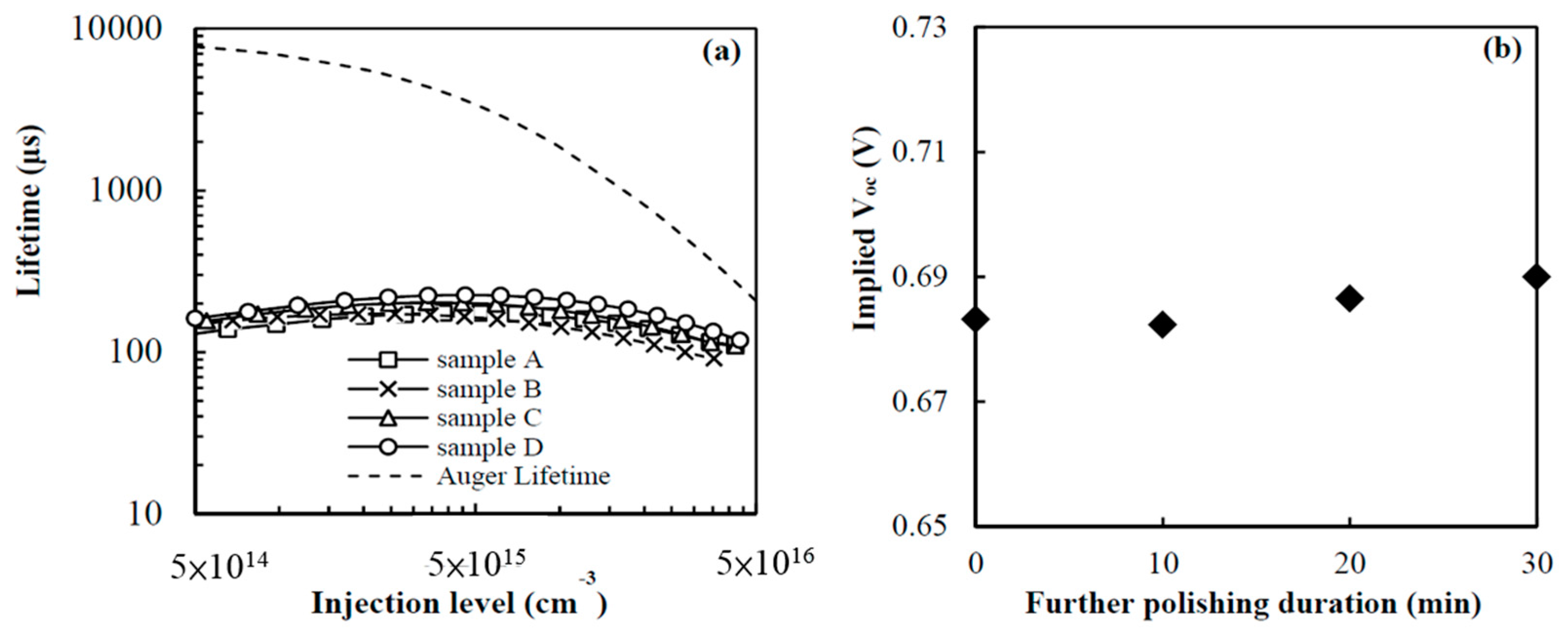
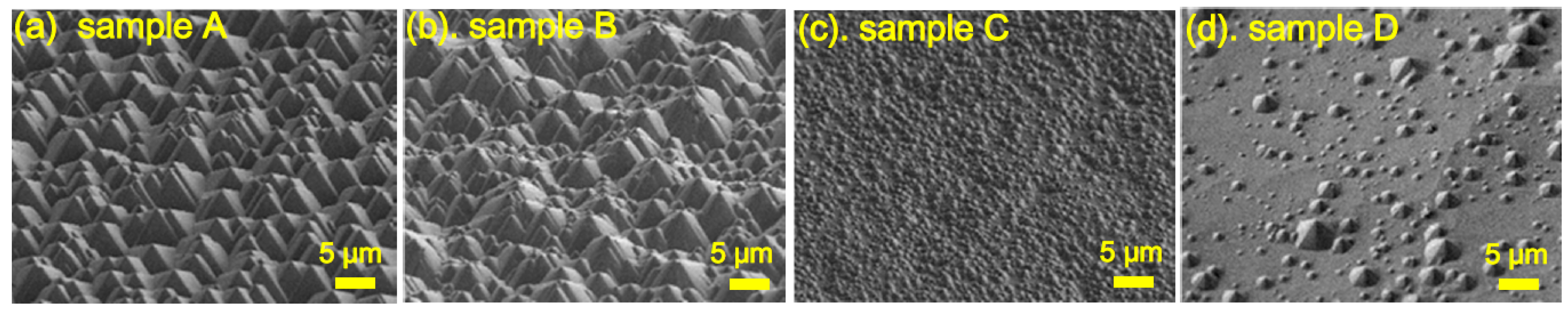
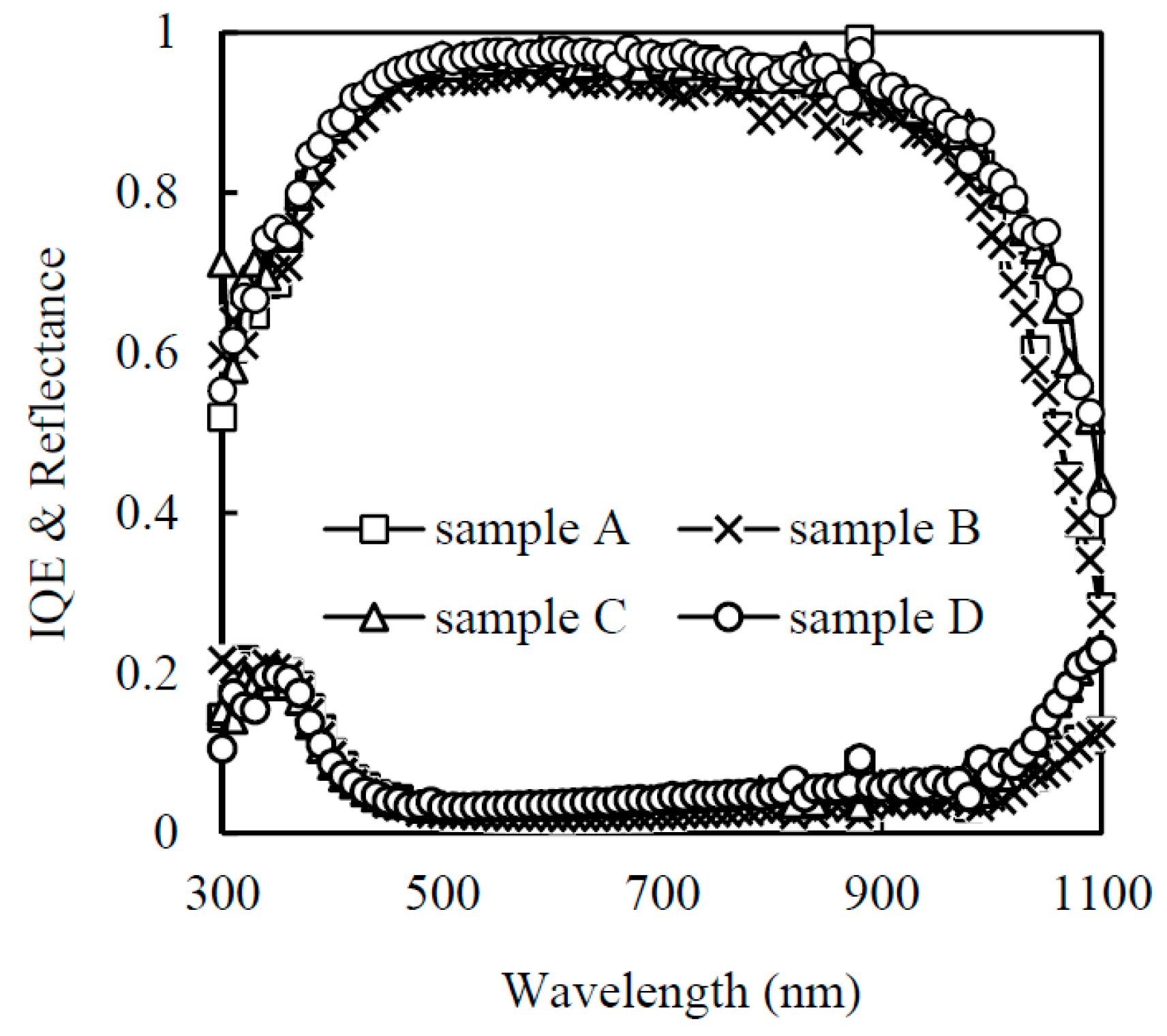
3. Results and Discussion

The XRD patterns of the Al2O3 films after annealing treatment from 350 °C to 650 °C are shown in Figure 1. The only (100) peaks, which represent crystalline silicon substrates, are observed in all samples. This result indicates that all the Al2O3 films are amorphous phase, and the thermal stability of the Al2O3 films are outstanding. In this study, Al2O3 films annealed at 450 °C are used, due to their longer lifetimes compared with Al2O3 films annealed at other temperatures. As the annealing temperature increases over 500 °C, the lifetime starts to decrease. Lifetime reduction at high annealing temperature has also been obtained by other research groups [9,10].
The rear-side surface morphologies for the samples treated with the standard texture process and further polishing processes for 10, 20, and 30 min are shown in Figure 2. The typical textured surface morphology containing uniformly sized pyramids of around 5 to 8 μm (width of the base) can be seen in Figure 2a. In Figure 2b, large and small pyramids start to coexist with the additional polishing process as the duration approaches 10 min. By extending the duration to 20 min, all the pyramids become uniformly smaller and thinner as shown in Figure 2c. Increasing the duration to 30 min produces a smoothed surface like a mirror; most pyramids almost disappear as seen in Figure 2d. Overall these four stages constitute a substantially texturing cycle.
Figure 3a shows the injection level dependent effective minority carrier lifetime and Auger lifetime for the four samples. The effective lifetime is calculated from the photoluminescence intensity by the self-consistent calibration method, and the Auger lifetime is calculated by the model proposed by Richter et al. [11]. The effective lifetime for samples A, B, C, and D are 174.4, 163.7, 200.1, and 225.3 µs at the injection level of 5 × 1015 cm−3, respectively. The 1-Sun lifetime values for sample A, B, C, and D are 170, 159.9, 194, and 212 µs, respectively. As the etching time increases, the lifetime decreases firstly and then increases to its saturation value when the wafer is fully polished. A lifetime drop in sample B can be attributed to the non-uniform pyramid structure with too many turning points (peaks and valleys of pyramids), which may cause film cracks. This damage traps carriers and reduces the lifetime. Another reason for the lower lifetime is related to a less efficient cleaning of the surface due to the presence of narrow valleys between pyramids. Two factors can account for the better performance of samples C and D. First, the polishing process not only smooths the wafer surface but also removes sawing damages, thereby reducing the surface recombination velocity. Second, since sample A and B both have larger rear-side surface areas than that of sample C and D, more defects are present at the Si/Al2O3 interface, acting as recombination centers. This result corresponds well with the observations from the SEM images. Sample D exhibits a slight increase in lifetime at an injection level of 5 × 1015 cm−3, which is more apparent than that observed for the other cells due to the superior field-effect passivation for the Al2O3 film on the mirror-like polished surface compared with that on the other rougher surfaces. At a low injection level, negligible minority carriers are generated to charge the inversion layer, and a shorter lifetime is gained due to the asymmetry in the electron and hole capture cross sections at the Si/Al2O3 interface [12]. With regard to higher injection levels, the lifetime starts to shorten with increasing Auger recombination. The implied Voc exported from the Sinton-120 lifetime tester (Sinton Instruments, Boulder, CO, USA) for the four samples are shown in Figure 3b to evaluate the maximum Voc before metal deposition. The implied Voc is extracted by the relation proposed by Sinton [13]:
τ e f f ( Δ n ) = Δ n ( t ) G Δ n ( t ) / Δ t
i m p l i e d   V oc = k T q l n ( Δ n ( N A + Δ n ) n i 2 )
where G is the generation rate; τeff is the effective minority carrier lifetime; ∆n is the excess carrier concentration; ∆t is the time taken in seconds; k is the Boltzmann constant; T is the temperature; NA is the acceptor concentration of the wafer; and ni is the intrinsic carrier concentration. The implied Voc following the same trend as the effective minority carrier lifetime with respect to the further polishing time can exactly predict the performance of the surface passivation for the fabricated PERCs, especially in Voc.
Figure 4 illustrates the reproducible illuminated J-V characteristics for all the PERCs. All of the curves are very close in this figure. The detailed solar cell external parameters are summarized in Table 1. Both Voc and Jsc are obviously affected by the rear-side surface, whereas the FF changes little in the range of 0.777 to 0.793, which is attributed to the probable experimental scattering. This reveals that the polishing process is beneficial for Voc and Jsc due to better surface passivation and long-wavelength reflection, respectively, but rarely influences the series resistance or shunt resistance. The most obvious variation of the electrical performance for each cell is in the Voc, proving that the polishing treatment plays a much more important role in preventing carrier recombination at the rear-side Si/A2O3 interface than gaining the long-wavelength light. Both relatively planar surfaces of samples C and D have Voc over 0.66 V and Jsc over 36.6 mA/cm2, while the further etching time exceeded 20 min. Note that the real Voc for all cells following the same trend as the implied Voc is evidence for reproducibility in this work. Overall, sample D demonstrates the optimized efficiency of 19.27%, with the Voc of 0.662 V, Jsc of 36.69 mA/cm2, and FF of 0.793.
The IQE and reflectance for the PERCs with different surface morphologies are shown in Figure 5. In the short wavelength range before 500 nm, the performance for each curve is similar. Samples C and D represent better spectral responses compared with the other samples at the middle wavelength range from 500 to 900 nm. This may be due to the relatively exceptional rear-side passivation provided by the Al2O3 films on the flatter surfaces; photogenerated electrons at the bottom of wafer are therefore easily repelled to the p-n junction for collection. This can be proven by calculating the effective diffusion length (Leff) using the method proposed by P. A. Basore [14]. The Leff for all samples is more than 1450 µm. As for the wavelengths over 900 nm, an obvious difference in spectral response occurs as well. The smoothed surface of sample D that is functionally analogous to a mirror facilitates the reflection of more unabsorbed long-wavelength light back to the active region of the Si bulk. Both reasons mentioned above make contributions to the higher Jsc of 36.69 mA/cm2 for sample D.

4. Conclusions

In this study, the performance of PERCs with different rear-side morphologies are investigated. Due to superior field-effect passivation and reabsorption of long-wavelength light, the fully polished sample D attains a longer effective lifetime (225.3 µs) and higher averaged rear-side reflectance (7.6%) in the long-wavelength range than the other PERCs. The polishing process improves the conversion efficiency from 18.62% to 19.27%, revealing that the polishing process enhances the performance of the PERCs. This study demonstrates the importance of an optimized rear-side polishing process for the industrial fabrication of PERC solar cells with higher efficiencies.

Acknowledgments

This work is sponsored by the Ministry of Science and Technology of the Republic of China under the grants No. 104-2632-E-212-002—Project supported by the Science and Technology Program of the Educational Office of Fujian Province, China (No. JB12182).

Author Contributions

Chih-Hsiang Yang and Shui-Yang Lien designed the experiments; Chih-Hsiang Yang, Chun-Wei Huang, Wen-Zhang Zhu, Hai-Jun Lin, and Xiao-Ying Zhang performed the experiments and measurements; Chung-Yuan Kung and Chih-Hsiang Yang analyzed the results; Chih-Hsiang Yang wrote the paper.

Conflicts of Interest

The authors declare no conflict of interest.

References

  1. Tanaka, M.; Taguchi, M.; Matsuyama, T.; Sawada, T.; Tsuda, S.; Nakano, S.; Hanafusa, H.; Kuwano, S. Development of new s-Si/c-Si heterojunction solar cells: ACJ-HIT (artificially constructed junction-heterojunction with intrinsic thin-layer). Jpn. J. Appl. Phys. 1992, 31, 3518. [Google Scholar] [CrossRef]
  2. Swanson, R.M.; Beckwith, S.K.; Crane, R.A.; Eades, W.D.; Kwark, Y.H.; Sinton, R.A.; Swirhun, S.E. Point-Contact Silicon Solar Cells. IEEE Trans. Electron Devices 1984, 31, 661–664. [Google Scholar] [CrossRef]
  3. Blakers, A.W.; Wang, A.; Milne, A.M.; Zhao, J.; Green, M.A. 22.8% efficient silicon solar cell. Appl. Phys. Lett. 1989, 55, 1363–1365. [Google Scholar] [CrossRef]
  4. Agostinelli, G.; Choulat, P.; Ma, Y.; Beaucarne, G. Thin Solar Cells: Issues and Processing for High Efficiency. In Proceedings of the 17th Workshop on Crystalline Silicon Solar Cells & Modules: Materials and Processes, Vail, CO, USA, 5–8 August 2007. [Google Scholar]
  5. Saint-Cast, P.; Kania, D.; Hofmann, M.; Benick, J.; Rentsch, J.; Preu, R. Very low surface recombination velocity on p-type c-Si by high-rate plasma-deposited aluminum oxide. Appl. Phys. Lett. 2009, 95, 151502. [Google Scholar] [CrossRef]
  6. Hoex, B.; Schmidt, J.; Bock, R.; Altermatt, P.P.; van de Sanden, M.C.M.; Kessels, W.M.M. Excellent passivation of highly doped p-type Si surfaces by the negative-charge-dielectric Al2O3. Appl. Phys. Lett. 2007, 91, 112107. [Google Scholar] [CrossRef]
  7. Kim, J.; Kim, J.; Lim, J.Y.; Hwang, Y.; Cho, J.; Choi, H.; Lee, E. Laser ablation of aluminum oxide and silicon nitride rear-side passivation for i-PERC cell. Renew. Energy 2015, 79, 135–139. [Google Scholar] [CrossRef]
  8. Hwang, Y.; Park, C.S.; Kim, J.; Kim, J.; Lim, J.Y.; Choi, H.; Jo, J.; Lee, E. Effect of laser damage etching on i-PERC solar cells. Renew. Energy 2015, 79, 131–134. [Google Scholar] [CrossRef]
  9. Kersten, F.; Schmid, A.; Bordihn, S.; Müller, J.W.; Heitmann, J. Role of Annealing Conditions on Surface Passivation Properties of ALD Al2O3 Films. Energy Procedia 2013, 38, 843–848. [Google Scholar] [CrossRef]
  10. Suh, D.; Liang, W.S. Electrical properties of atomic layer deposited Al2O3 with anneal temperature for surface passivation. Thin Solid Films 2013, 539, 309–316. [Google Scholar] [CrossRef]
  11. Richter, A.; Glunz, S.W. Improved quantitative description of Auger recombination in crystalline silicon. Phys. Rev. B 2012, 86, 165202. [Google Scholar] [CrossRef]
  12. Lu, P.H.; Wang, K.; Lu, Z.; Lennon, A.J.; Wenham, S.R. Anodic Aluminum Oxide Passivation For Silicon Solar Cells. IEEE J. Photovolt. 2013, 3, 143–151. [Google Scholar] [CrossRef]
  13. Wang, H.P.; Li, A.C.; Lin, T.Y.; He, J.H. Concurrent improvement in optical and electrical characteristics by using inverted pyramidal array structures toward efficient Si heterojunction solar cells. Nano Energy 2016, 23, 1–6. [Google Scholar] [CrossRef]
  14. Basore, P.A. Extended spectral analysis of internal quantum efficiency. In Proceedings of the Conference Record of the Twenty Third IEEE Photovoltaic Specialists Conference, Louisville, KY, USA, 10–14 May 1993; pp. 147–152. [Google Scholar]
Figure 1. XRD patterns of the Al2O3 films annealed at various temperatures.
Applsci 07 00410 g001
Figure 2. EM images of rear-side of the silicon wafers with further polishing duration for: (a) 0; (b) 10; (c) 20; (d) 30 min.
Applsci 07 00410 g002
Figure 3. (a) Effective lifetime as a function of injection level; (b) Implied Voc for the Al2O3 films with different rear-side surface morphologies.
Applsci 07 00410 g003
Figure 4. J-V characteristics for both the PERCs (passivated emitter and rear cells) with different rear-side surface morphologies.
Applsci 07 00410 g004
Figure 5. IQE (internal quantum efficiency) and reflectance for the PERCs deposited on Si wafers with different rear-side surface morphologies.
Applsci 07 00410 g005
Table 1. The detailed electrical external parameters for all PERCs (passivated emitter and rear cells).
SampleVoc (V)Jsc (mA/cm2)FFEfficiency (%)
A0.65536.470.77918.62
B0.64836.430.78918.64
C0.66036.640.77718.80
D0.66236.690.79319.27

