
Demonstration of High-Speed Optical Transmission at 2 µm in Titanium Dioxide Waveguides


Laboratoire Interdisciplinaire Carnot de Bourgogne (ICB), UMR 6303 CNRS–Université de Bourgogne Franche-Comté, 9 Avenue Alain Savary, BP 47870, 21078 Dijon CEDEX, France
*
Author to whom correspondence should be addressed.
Appl. Sci. 2017, 7(6), 631; https://doi.org/10.3390/app7060631
Submission received: 16 May 2017
/
Revised: 12 June 2017
/
Accepted: 15 June 2017
/
Published: 17 June 2017
(This article belongs to the Special Issue Guided-Wave Optics)
Abstract
:We demonstrate the transmission of a 10-Gbit/s optical data signal in the 2 µm waveband into titanium dioxide waveguides. Error-free transmissions have been experimentally achieved taking advantage of a 23-dB insertion loss fiber-to-fiber grating-based injection test-bed platform.
1. Introduction
Nowadays, optical communication traffic continuously increases, inexorably approaching a “capacity crunch” [1,2,3]: the conventional C-band around 1.55 µm will not be sufficient anymore and alternative approaches have to be adopted [4]. Recently, the 2 µm spectral region has been suggested as a new transmission window [5], benefiting from the emergence of thulium-doped fiber amplifiers (TDFA) with broadband and high gain spanning from 1900 to 2100 nm [6]. This has stimulated studies of dedicated photonic components such as InP-based modulators [7,8] or arrayed waveguide gratings [9]. High bit rate communications over distances exceeding one hundred meters have already been successfully demonstrated [10,11,12,13] in low-loss hollow core bandgap photonic fibers designed to present minimal losses around 2000 nm [14] or in solid-core single mode fibers [15].
Optical transmissions over much shorter distances (typically a few hundred micrometers) also deserve interest in the context of on-board connections and photonic routing operations. Therefore, this open issue requires further experimental investigations to evaluate the potential of various materials transparent in this new spectral band. Optimally, such a material should be also transparent in other telecommunication bands ranging from O-band (1310 nm) to C-band (1550 nm) and eventually also in the 850-nm band. Regarding the recent research, a natural choice could be silicon nitride (Si3N4), which has already stimulated many works in the visible but also in the mid-infrared range, mainly in the context of frequency combs [16]. In this new contribution, we are interested in another material which remains to date relatively unexplored: titanium dioxide (TiO2). This cost-efficient material is indeed transparent from visible to mid-infrared wavelengths [17] and can be considered as a complementary metal-oxide semiconductor (CMOS) compatible material [18]. Compared to Si3N4, TiO2 presents several advantages. Among them, it presents lower stress constraints for thicknesses beyond 250 nm and has an easier deposition process possible at lower temperatures. Note also that it exhibits a higher linear refractive index, which is critical for a stronger confinement [19]. Up to now, detailed studies have taken advantage of its negative thermo-optic coefficient [18,20] and its transparency in the visible range [21,22], or have reported on its linear and nonlinear properties in the C-band [19,23,24]. In this work, we experimentally explore, for the first time, TiO2 as an efficient medium for a photonic component operating at 2 µm. After describing the design and fabrication of our TiO2 waveguides, we detail the experimental setup under use and validate the device for error-free transmission of a 10 Gbit/s on-off keying signal for both a subwavelength single mode waveguide and a multimode waveguide.
2. Design and Fabrication of the Photonic Structure
2.1. Design and Fabrication of the Photonic Structure
Whatever the platform involved for the design, a critical issue in integrated photonics is always how to efficiently couple the light into the device. In a dedicated article [25], we recently investigated and experimentally validated a new kind of metal grating that is embedded directly within the dielectric layer instead of being deposited on it [26]. Thus, we were able to efficiently couple a 1.55 µm signal into a TiO2 photonic waveguide. Here, a similar design is exploited, as depicted in Figure 1a. More precisely, the structure consists of a metal (Au) grating embedded between two TiO2 layers on a glass substrate.
Using a commercial finite element-based software (Comsol Multiphysics), we can optimize the parameters of the design to obtain the best coupling around the 2 µm wavelength. We have taken into account the fabrication and experimental setup constraints, leading to fixed values for the bottom layer height hbottom = 70 nm and of the incident angle Θ = 30°. Thus, using a Monte Carlo algorithm varying (hAu, htop, Λ, w1) in a 4D parameter space, the coupling efficiency could reach 52% for transverse magnetic (TM) mode when the gold height hAu = 57 nm, the top layer height htop = 234 nm, the period Λ = 1904 nm, and the width of grating lines w1 = 980 nm. However, with these parameters, the coupling efficiency for the transverse electric (TE) mode drops down to 10%. Similarly, the optimization of parameters for the TE mode gives an efficiency reaching up to 36% for hAu = 45 nm, htop = 234 nm, Λ = 1679 nm, and w1 = 356 nm, whereas those parameters give a poor efficiency of 1% for the TM mode.
However, contrary to Reference [25], our aim is not to reach the best coupling efficiency. Here, we tried to find numerically the geometric parameters that allow a fair coupling efficiency in both the TE and TM modes for a slab. From the previous optimization, the top layer should be 234 nm and, given that hbottom = 70 nm, the total TiO2 thickness considered is 304 nm. The thickness of the gold lines hAu is chosen to be 56 nm, while the period Λ = 1900 nm. To adjust the efficiency of the TM mode compared to the TE mode, we adjust the filling factor by sequentially varying the width w1, as shown in Figure 1b. It appears that three values of w1 allow a similar coupling for the TE and TM modes, but the width of the grating lines that gives the best efficiency (−8.5 dB) is around 700 nm.
2.2. Modal Analysis
Here, we focus our attention on two strip waveguides (Figure 2a): an 8.0-µm wide waveguide and a subwavelength 1.6-µm wide waveguide. The 8-µm wide waveguide is clearly multimode with nine TE modes and three TM modes. Considering a refractive index of 1.44 for the glass substrate and 2.41 for the TiO2 layer [17], Figure 2b shows that the first TE and TM modes in the multimode (MM) waveguide have an effective index of 1.87 and 1.49, respectively. Note that the TM mode is clearly much less confined than the TE mode, as can be seen in Figure 2(b2), but over the length considered, the lossy behavior of the TM mode has very low impact, as demonstrated in the following sections. The subwavelength 1.6-µm wide waveguide is single-mode (SM) with an effective index of the TE mode around 1.78, shown in Figure 2c.
2.3. Fabrication
The fabrication process relies on traditional techniques. Titanium dioxide layers are deposited on a glass substrate by reactive direct current (DC) magnetron sputtering of a 99.9% pure titanium target under argon and oxygen control atmosphere. Electron-beam lithography, followed by thermal gold evaporation (here, 3 nm of chromium are used as an adhesion layer) and a lift-off process is used to fabricate the gold gratings. Then the top layer of TiO2 is deposited, followed by overlay electron-beam lithography. After metallic mask evaporation, reactive ion etching is performed to make the waveguides. Finally, wet etching removes the mask to obtain the final device to be tested.
As mentioned previously, we fabricated two structures of interest (Figure 3): an MM waveguide (with a width of 8 µm) and an SM waveguide (slightly overexposed leading to a width of 1.65 µm).
These waveguides have the same length fixed at 575 µm but, for the SM waveguide, two 85-µm long tapers (with a maximal width of 30 µm) are used at the input and output. The parameters measured on the fabricated device differ slightly from the targeted one: we measured a 304-nm total thicknesss with hbottom = 69 nm and htop = 235 nm. Moreover, the waveguide width is actually 1.65 µm, which induces the existence of the TE0,1 with an effective index close to 1.47. For each structure, two widths of grating lines (related to filling factor) have been fabricated. The two targeted widths were the best values for which TE and TM were equal in Figure 1b (i.e., 550 and 700 nm). However, due to overexposure, we measured both widths to be 630 and 860 nm.
2.4. Test of the Device
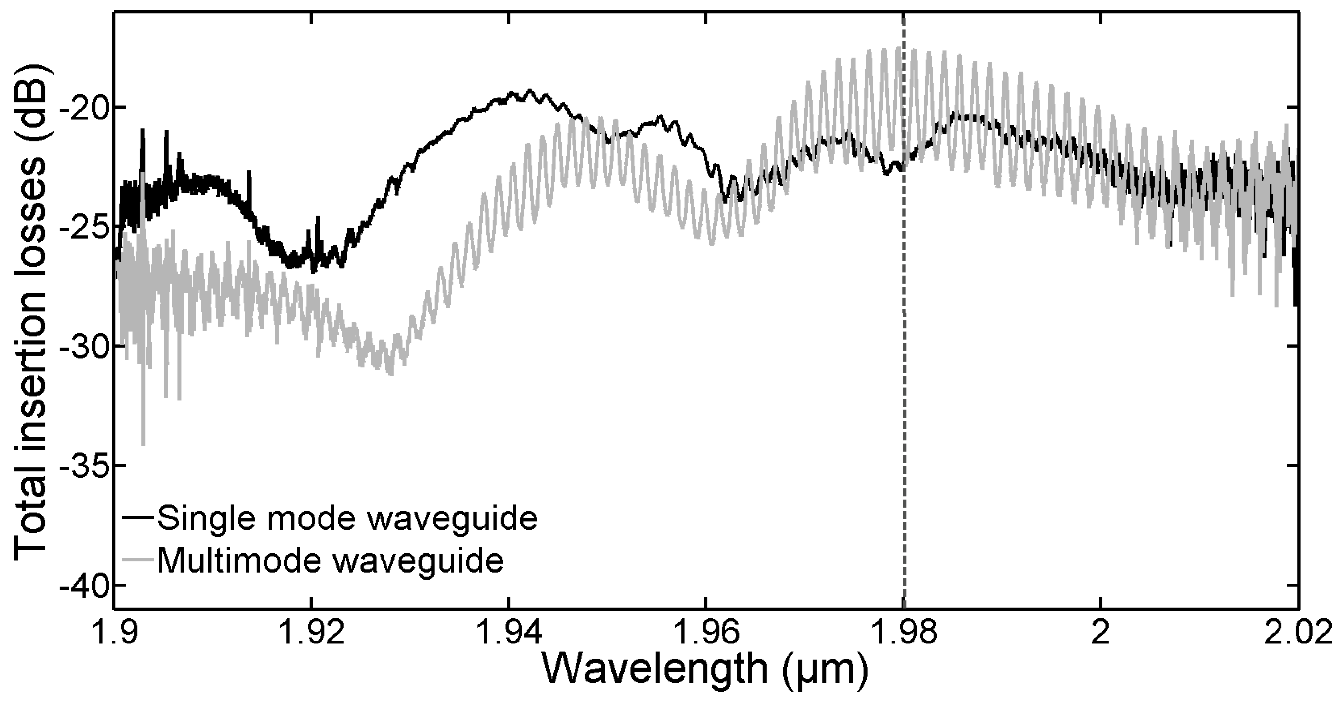
We then characterized the coupling efficiency of the waveguides with a setup similar as in Reference [25]. Two focusers oriented with an angle of 30° were used to inject and collect the signal at the input and output gratings, respectively. The injection of light emitted by an amplified spontaneous emission (ASE) source spanning from 1900 to 2050 nm was adjusted (thanks to two cameras operating in the visible and 2-µm ranges (model Xeva 2.35-320, Xenics nv, Leuven, Belgium). After transmission in the waveguide and decoupling by the grating, the output light was collected by a lensed-fiber focuser and recorded with an optical spectrum analyzer (OSA) (model AQ6375B, Yokogawa Electric Corporation, Musashino, Japan). Figure 4 shows the total insertion losses as a function of the injected wavelength for the two waveguides under test. Note that those transmission spectra are normalized with respect to a reference spectrum obtained by optimizing the light collected by the output focuser after specular reflection of the incident light onto a gold mirror [25]. It is noted that, in Figure 4, oscillations of high amplitude and short period are particularly marked for the large waveguide. These spectral oscillations are attributed to a Fabry–Perot effect, the spectral range between two maxima being in agreement with what can be expected from the roundtrip distance. The experimental loss should be twice as large as the value expected from our numerical simulation (Figure 1) performed for one facet, given that we neglect the propagation loss. Then, the discrepancy between the numerical simulations and the maximum experimental efficiency is about 3 dB, mainly attributed to the strong dependency on the width of the grating lines and also probably due to fabrication issues (in particular related to the roughness). Even though, for the MM waveguide configuration, the TE mode was expected to be as efficient as the TM mode for a grating line width of 700 nm, here it was the case for w1 = 630 nm. Regarding the TE SM waveguide, as expected, the coupling efficiency is similar to the one obtained for the large waveguide. Let us once again recall that a (6 dB) better efficiency can be reached for optimized parameters, but our goal here was to establish a fair comparison between the MM and SM components.
3. Validation of the Transmission of a 10 Gbit/s Signal
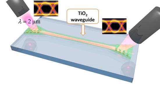
In order to demonstrate the suitability of our TiO2 devices for 2-µm optical communications, we implemented the experimental setup detailed in Figure 5, based on 2-µm commercially available devices. The transmitter (TX) was based on a laser diode centered at 1980 nm and was intensity modulated by means of a commercial Niobate–Lithium modulator (model MX2000-LN-10, iXblue Photonics, Besançon, France). The Non-Return-to-Zero On-Off-Keying signal under test was a 231–1 pseudorandom bit sequence (PRBS) at 10 Gbit/s. Since the SM waveguide is polarization-sensitive, a polarization controller was used after the intensity modulator. Then, a thulium-doped fiber amplifier (TDFA) was used before a 90/10 coupler, allowing us to monitor the power injected into the waveguide. Note that the variable optical attenuator is usually implemented just in front of the receiver, but due to limited sensitivity of the available power meters working at 2 µm, it was more convenient to insert it before the waveguide.
The receiver (RX) was based on a second TDFA. This TDFA was set to work with a constant gain instead of a constant output power, as usually used in C-band. Therefore, a variable optical attenuator was implemented at its output to ensure that the photodiode operated at a constant power level. An optical bandpass filter (0.64 nm bandwidth) (model OETFG-100, O/E Land Inc., LaSalle, QC, Canada) was also inserted at the output of the system, in order to limit the accumulation of amplified spontaneous emission from the TDFAs. The signal was finally analyzed both in the spectral and temporal domains. An optical spectrum analyzer was used to measure the optical signal-to-noise ratio (OSNR) of the received signal (using the usual 0.1 nm noise bandwidth), whereas a photodiode (12.5 GHz electrical bandwidth) (model 818-BB-51F, Newport corporation, Irvine, CA, USA) enabled bit error rate measurements in addition to recording of the output eye diagram on a high-speed sampling oscilloscope.
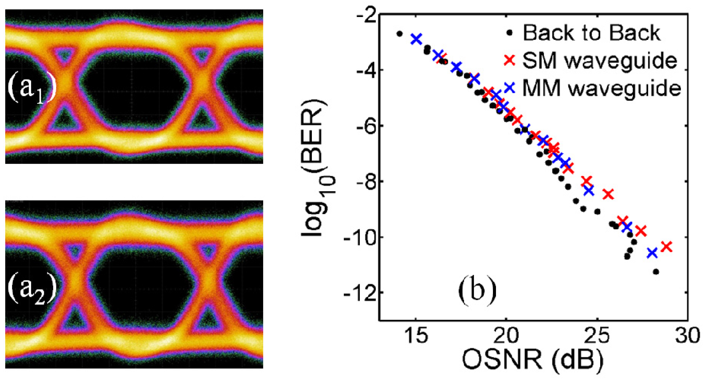
Figure 6 summarizes the results obtained at 1980 nm. Error-free operation can be achieved for back-to-back measurements as well as in the presence of the TiO2 waveguides. Examples of the corresponding eye-diagrams are provided in panels (a): in both configurations, a widely open eye can be recorded and the insertion of the waveguides under test does not induce any visible degradations of the transmission.
The quality of the transmission through the TiO2 waveguide was more quantitatively evaluated through systematic measurements of the Bit-Error-Rate according to the OSNR on the receiver. The results obtained for the various configurations are summarized in Figure 6b. From a general point of view, the global trends are very similar, with very moderate penalty (~1.5 dB) obtained after transmission through the waveguides and compared to the back-to-back configuration for BER lower than 10−8. Moreover, no significant difference was observed between the SM and MM waveguides. Therefore, for the length of propagation under consideration, the multimode nature of the waveguide does not seem to impair the transmission quality.
Before concluding, we would like to emphasize here the fact that such measurements are not as straightforward as in the C-band. Indeed, the 2-µm devices have not reached the same level of maturity and it is still difficult to find such devices commercially available. This experiment shows that despite the lack of optimized devices, error-free transmission is possible, confirming that this new waveband is definitely an effective alternative, especially if new solutions appear in the next few years.
4. Conclusions
To conclude (thanks to embedded metal gratings) we have been able to efficiently couple an incident light beam into a TiO2 waveguide in the 2-µm spectral range. This particular design allows us to demonstrate, for the first time, an error-free transmission of a 2-µm optical data stream at 10 Gbit/s in a 575-µm long TiO2 waveguide. A full set of BER measurements has been performed with a fair comparison between a single-mode 1.65-µm wide waveguide and a multimode 8-µm wide waveguide insensitive to the polarization. No significant difference was then observed. With the future progress of the emitter/receiver stages, we believe that the present component will also be able to handle higher transmission speeds.
This study paves the way to integrated photonics at 2 µm, and introduces titanium dioxide as a serious candidate for photonics from the visible to the mid-infrared range. With technological progress and the maturity gain that can be expected in the near future for fiber and optoelectronics solutions operating around 2 µm, we are confident in the possibility of involving longer TiO2 waveguides up to a few centimeters in length.
Acknowledgments
This work is financially supported by PARI PHOTCOM Région Bourgogne, by Carnot Arts Institute (PICASSO 2.0 project), by the Institut Universitaire de France, and by FEDER-FSE Bourgogne 2014/2020. The research work has benefited from the PICASSO experimental platform of the University of Burgundy. We thank M. G. Nielsen for advices and fruitful discussions on the grating design issues.
Author Contributions
Manon Lamy, Kamal Hammani, Christophe Finot and Julien Fatome conceived, designed and performed the experiment of optical transmission; Manon Lamy, Kamal Hammani, Juan Arocas and Jean-Claude Weeber designed and fabricated the optical waveguides and the associated gratings. Manon Lamy, Kamal Hammani and Jean-Claude Weeber took part in the numerical modelling and interpretation. All the authors contribute to the analysis of the results and to the writing of the manuscript. Kamal Hammani and Christophe Finot supervised the project.
Conflicts of Interest
The authors declare no conflict of interest.
References
- Richardson, D.J. Filling the light pipe. Science 2010, 330, 327–328. [Google Scholar] [CrossRef] [PubMed]
- Ellis, A.D.; Suibhne, N.M.; Saad, D.; Payne, D.N. Communication networks beyond the capacity crunch. Philos. Trans. R. Soc. A 2016, 374. [Google Scholar] [CrossRef] [PubMed]
- Desurvire, E.B. Capacity demand and technology challenges for lightwave systems in the next two decades. J. Lightwave Technol. 2006, 24, 4697–4710. [Google Scholar] [CrossRef]
- Richardson, D.J. New optical fibres for high-capacity optical communications. Philos. Trans. R. Soc. A 2016, 374. [Google Scholar] [CrossRef] [PubMed]
- Kavanagh, N.; Sadiq, M.; Shortiss, K.; Zhang, H.; Thomas, K.; Gocalinska, A.; Zhao, Y.; Pelucchi, E.; Brien, P.O.; Peters, F.H.; et al. Exploring a new transmission window for telecommunications in the 2 µm waveband. In Proceedings of the 18th International Conference on Transparent Optical Networks (ICTON 2016), Trento, Italy, 10–14 July 2016; pp. 1–4. [Google Scholar]
- Li, Z.; Heidt, A.M.; Daniel, J.M.O.; Jung, Y.; Alam, S.U.; Richardson, D.J. Thulium-doped fiber amplifier for optical communications at 2 µm. Opt. Express 2013, 21, 9289–9297. [Google Scholar] [CrossRef] [PubMed]
- Ye, N.; Gleeson, M.R.; Sadiq, M.U.; Roycroft, B.; Robert, C.; Yang, H.; Zhang, H.; Morrissey, P.E.; Mac Suibhne, N.; Thomas, K.; et al. InP-based active and passive components for communication systems at 2 μm. J. Lightwave Technol. 2015, 33, 971–975. [Google Scholar] [CrossRef]
- Sadiq, M.U.; Gleeson, M.R.; Ye, N.; O′Callaghan, J.; Morrissey, P.; Zhang, H.Y.; Thomas, K.; Gocalinska, A.; Pelucchi, E.; Gunning, F.C.G.; et al. 10 Gb/s InP-based Mach–Zehnder modulator for operation at 2 μm wavelengths. Opt. Express 2015, 23, 10905–10913. [Google Scholar] [CrossRef] [PubMed]
- Zhang, H.; Gleeson, M.; Ye, N.; Pavarelli, N.; Ouyang, X.; Zhao, J.; Kavanagh, N.; Robert, C.; Yang, H.; Morrissey, P.E.; et al. Dense WDM transmission at 2 µm enabled by an arrayed waveguide grating. Opt. Lett. 2015, 40, 3308–3311. [Google Scholar] [CrossRef] [PubMed]
- Petrovich, M.N.; Poletti, F.; Wooler, J.P.; Heidt, A.M.; Baddela, N.K.; Li, Z.; Gray, D.R.; Slavík, R.; Parmigiani, F.; Wheeler, N.V.; et al. Demonstration of amplified data transmission at 2 µm in a low-loss wide bandwidth hollow core photonic bandgap fiber. Opt. Express 2013, 21, 28559–28569. [Google Scholar] [CrossRef] [PubMed]
- Zhang, H.; Kavanagh, N.; Li, Z.; Zhao, J.; Ye, N.; Chen, Y.; Wheeler, N.V.; Wooler, J.P.; Hayes, J.R.; Sandoghchi, S.R.; et al. 100 Gbit/s WDM transmission at 2 µm: Transmission studies in both low-loss hollow core photonic bandgap fiber and solid core fiber. Opt. Express 2015, 23, 4946–4951. [Google Scholar] [CrossRef] [PubMed]
- Hayes, J.R.; Sandoghchi, S.R.; Bradley, T.D.; Liu, Z.; Slavik, R.; Gouveia, M.A.; Wheeler, N.V.; Jasion, G.T.; Chen, Y.; Numkam-Fokoua, E.; et al. Antiresonant hollow core fiber with octave spanning bandwidth for short haul data communications. In Proceedings of the OFC Conference Postdeadline Papers: p Th5A.3, Anaheim, CA, USA, 20 March 2016. [Google Scholar]
- Liu, Z.; Chen, Y.; Li, Z.; Kelly, B.; Phelan, R.; O’Carroll, J.; Bradley, T.; Wooler, J.P.; Wheeler, N.V.; Heidt, A.M.; et al. High-capacity directly modulated optical transmitter for 2 µm spectral region. J. Lightwave Technol. 2015, 33, 1373–1379. [Google Scholar] [CrossRef]
- Roberts, P.J.; Couny, F.; Sabert, H.; Mangan, B.J.; Williams, D.P.; Farr, L.; Mason, M.W.; Tomlinson, A.; Birks, T.A.; Knight, J.C.; et al. Ultimate low loss of hollow-core photonic crystal fibres. Opt. Express 2005, 13, 236–244. [Google Scholar] [CrossRef] [PubMed]
- Xu, K.; Sun, L.; Xie, Y.; Song, Q.; Du, J.; He, Z. Transmission of IM/DD signals at 2 μm wavelength using PAM and CAP. IEEE Photonics J. 2016, 8, 1–7. [Google Scholar] [CrossRef]
- Luke, K.; Okawachi, Y.; Lamont, M.R.E.; Gaeta, A.L.; Lipson, M. Broadband mid-infrared frequency comb generation in a Si3N4 microresonator. Opt. Lett. 2015, 40, 4823–4826. [Google Scholar] [CrossRef] [PubMed]
- Kischkat, J.; Peters, S.; Gruska, B.; Semtsiv, M.; Chashnikova, M.; Klinkmüller, M.; Fedosenko, O.; Machulik, S.; Aleksandrova, A.; Monastyrskyi, G.; et al. Mid-infrared optical properties of thin films of aluminum oxide, titanium dioxide, silicon dioxide, aluminum nitride, and silicon nitride. Appl. Opt. 2012, 51, 6789–6798. [Google Scholar] [CrossRef] [PubMed]
- Shang, K.; Djordjevic, S.S.; Li, J.; Liao, L.; Basak, J.; Liu, H.-F.; Yoo, S.J.B. Cmos-compatible titanium dioxide deposition for athermalization of silicon photonic waveguides. In Proceedings of the Optical Society of America CLEO: 2013, San Jose, CA, USA, 9 June 2013. [Google Scholar]
- Bradley, J.D.B.; Evans, C.C.; Choy, J.T.; Reshef, O.; Deotare, P.B.; Parsy, F.; Phillips, K.C.; Lončar, M.; Mazur, E. Submicrometer-wide amorphous and polycrystalline anatase TiO2 waveguides for microphotonic devices. Opt. Express 2012, 20, 23821–23831. [Google Scholar] [CrossRef] [PubMed]
- Reshef, O.; Shtyrkova, K.; Moebius, M.G.; Griesse-Nascimento, S.; Spector, S.; Evans, C.C.; Ippen, E.; Mazur, E. Polycrystalline anatase titanium dioxide microring resonators with negative thermo-optic coefficient. J. Opt. Soc. Am. B 2015, 32, 2288–2293. [Google Scholar] [CrossRef]
- Choy, J.T.; Bradley, J.D.B.; Deotare, P.B.; Burgess, I.B.; Evans, C.C.; Mazur, E.; Lončar, M. Integrated tio2 resonators for visible photonics. Opt. Lett. 2012, 37, 539–541. [Google Scholar] [CrossRef] [PubMed]
- Häyrinen, M.; Roussey, M.; Säynätjoki, A.; Kuittinen, M.; Honkanen, S. Titanium dioxide slot waveguides for visible wavelengths. Appl. Opt. 2015, 54, 2653–2657. [Google Scholar] [CrossRef] [PubMed]
- Evans, C.C.; Liu, C.; Suntivich, J. Low-loss titanium dioxide waveguides and resonators using a dielectric lift-off fabrication process. Opt. Express 2015, 23, 11160–11169. [Google Scholar] [CrossRef] [PubMed]
- Evans, C.C.; Shtyrkova, K.; Bradley, J.D.B.; Reshef, O.; Ippen, E.; Mazur, E. Spectral broadening in anatase titanium dioxide waveguides at telecommunication and near-visible wavelengths. Opt. Express 2013, 21, 18582–18591. [Google Scholar] [CrossRef] [PubMed]
- Lamy, M.; Hammani, K.; Arocas, J.; Finot, C.; Weeber, J. Broadband Metal Grating Couplers Embedded in Titanium Dioxide Waveguides. 2017. Available online: https://hal.archives-ouvertes.fr/hal-01503970 (accessed on 9 June 2017).
- Scheerlinck, S.; Schrauwen, J.; Van Laere, F.; Taillaert, D.; Van Thourhout, D.; Baets, R. Efficient, broadband and compact metal grating couplers for silicon-on-insulator waveguides. Opt. Express 2007, 15, 9625–9630. [Google Scholar] [CrossRef] [PubMed]
Figure 1.
(a) Embedded metal gratings in TiO2 layout; (b) Numerical simulations of the coupling efficiency for one facet as a function of the width w1 of the grating lines for the following parameters: hbottom = 70 nm, hAu = 5 nm, htop = 234 nm, Λ = 1900 nm at the central wavelength of our laser source (1.98 µm). The results for the transverse electric (TE) mode are compared to those for the transverse magnetic (TM) mode. The circles highlight the values where the efficiencies of both modes are equal. The green circle corresponds to the best value; (c) Corresponding coupling efficiency per facet for the TE and TM modes as a function of the wavelength (for w1 = 700 nm—green circle on panel (b)).
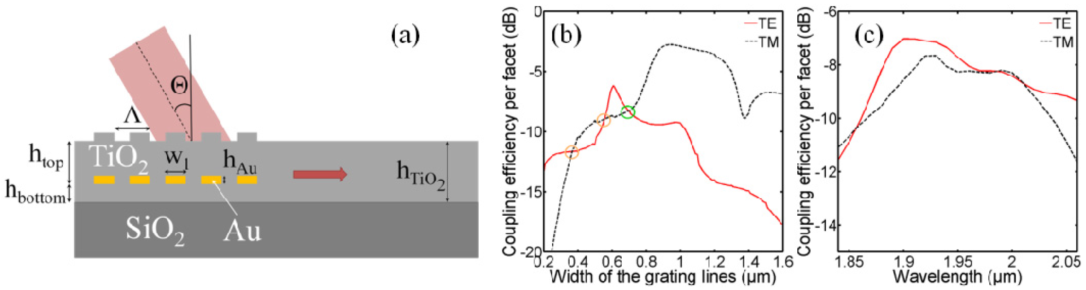
Figure 2.
(a) Sketch of the cross-section of the 304-nm strip waveguides. Corresponding mode profile of the electric field and associated effective index for (b) a multimode waveguide (width, 8 µm) and (c) a subwavelength waveguide (width, 1.6 µm). Subplot (b1) corresponds to the fundamental TE mode, whereas subplot (b2) is related to fundamental TM mode.
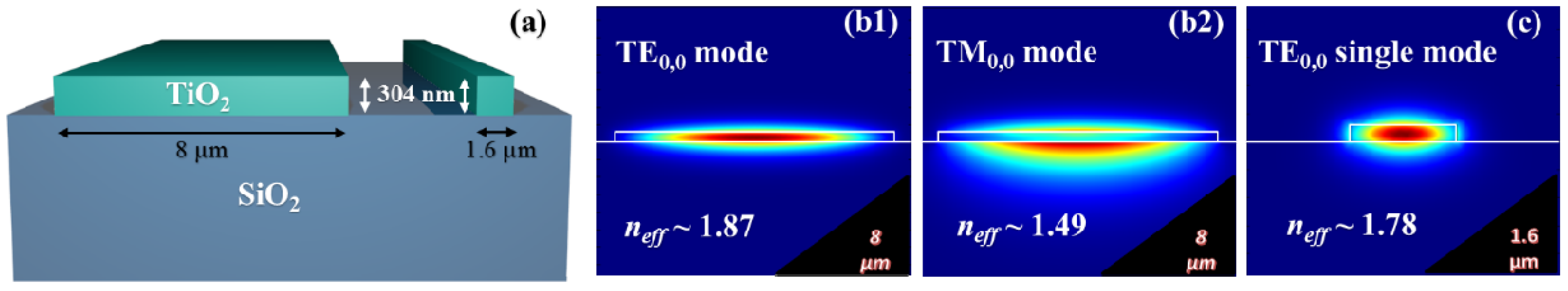
Figure 3.
Images of (a) a subwavelength waveguide and (b) a large waveguide considered as a slab. Insets 1 show scanning electron microscopy (SEM) pictures of embedded metal grating on one end of the waveguides whereas insets 2 show optical images of the waveguides. Contrary to the slab, the subwavelength waveguide is equipped with tapers. Insets 3 correspond to SEM pictures of the subwavelength that has a width of 1.65 µm (a3), and the slab which is actually 8.0 µm wide (b3).
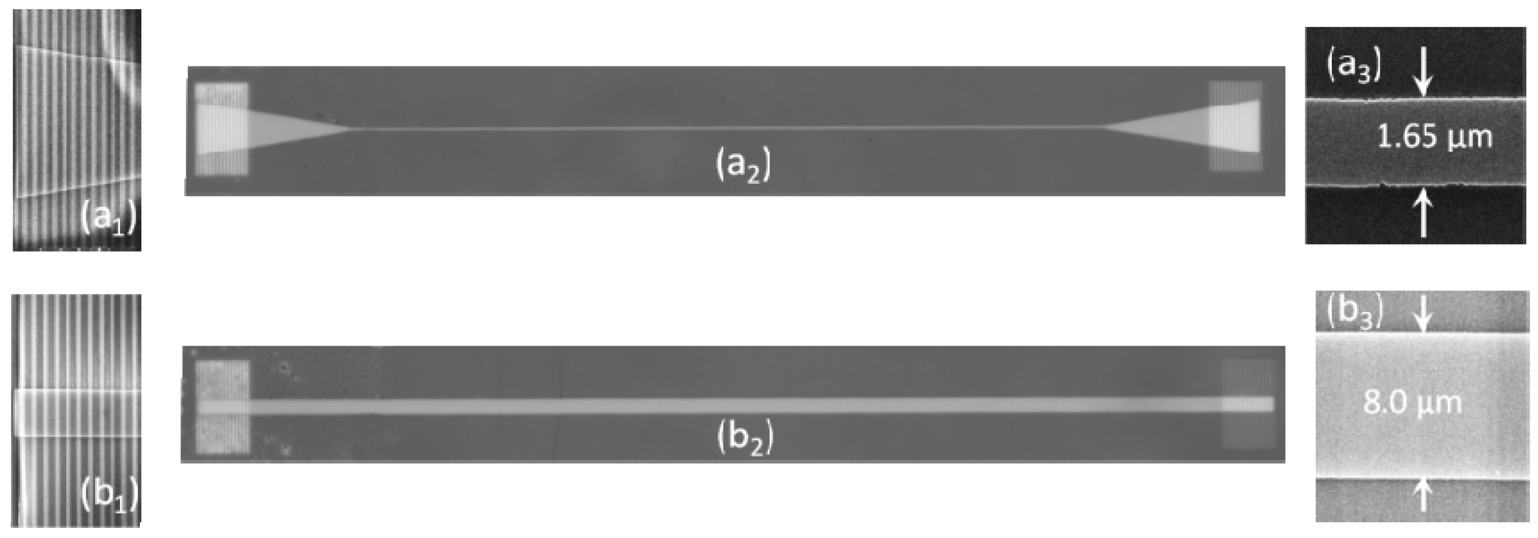
Figure 4.
Total insertion losses as a function of the injected wavelength for an MM waveguide (grey curve) and an SM waveguide (black curve) obtained with the amplified spontaneous emission (ASE) source (for w1 = 630 nm). The oscillations of short period on the grey curve are due to a Perot–Fabry effect. The grey dashed line corresponds to the central wavelength of the laser source used in the next section.

Figure 5.
Experimental setup for a 10-Gbit/s 2-µm optical transmission. CW: continuous wave; IM: intensity modulator; PC: polarization controller; PRBS: pseudorandom binary sequence; TDFA: thulium-doped fiber amplifier; VOA: variable optical attenuator; PM: power meter; OSA: optical spectrum analyzer; PD: photodiode; BERT: bit error rate tester (model MU181040A, Anritsu Corporation, Atsugi-shi, Japan).
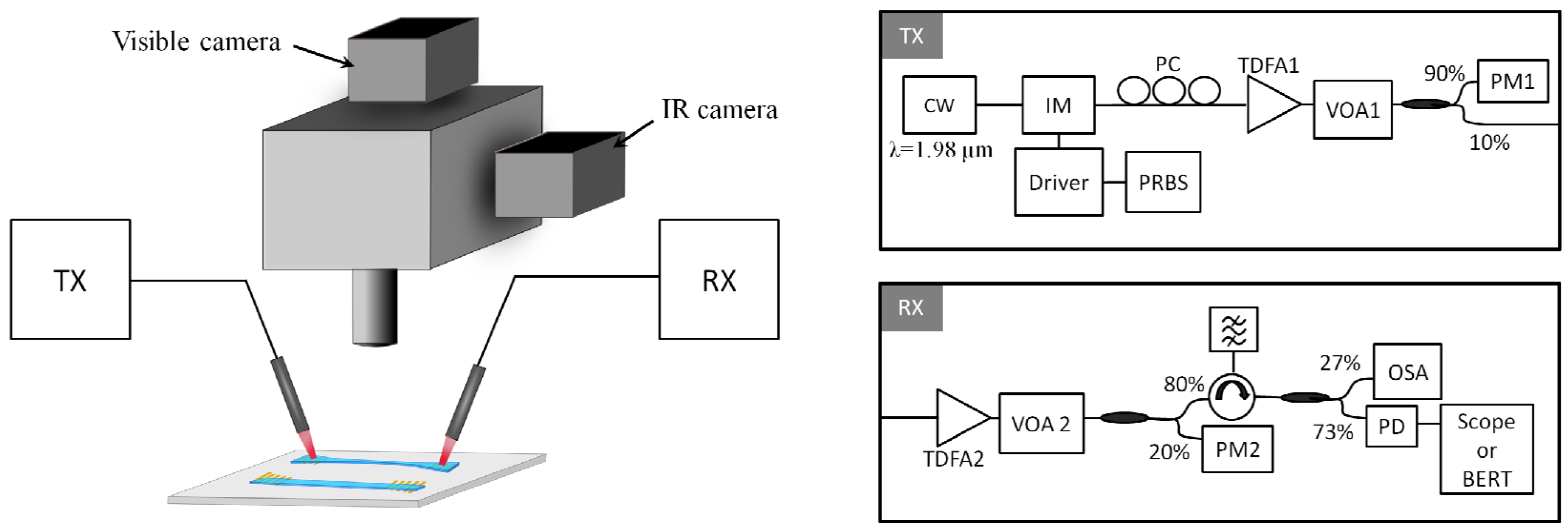
Figure 6.
(a) Eye diagrams for the back-to-back configuration and after transmission in the 1.65 μm wide waveguide (panels 1 and 2 respectively). In both cases, eyes diagrams were recorded for error-free measurements; (b) Bit-Error-Rate (BER) as a function of optical signal-to-noise ratio (OSNR) for the two previously described waveguides. On the graph, the black points of measurements are associated with back-to-back configuration. The crosses are used for BER measurements for TiO2 devices (red for the 1.65-µm SM wide waveguide and blue for the 8-µm wide MM waveguide).
© 2017 by the authors. Licensee MDPI, Basel, Switzerland. This article is an open access article distributed under the terms and conditions of the Creative Commons Attribution (CC BY) license (http://creativecommons.org/licenses/by/4.0/).
Share and Cite
MDPI and ACS Style
Lamy, M.; Finot, C.; Fatome, J.; Arocas, J.; Weeber, J.-C.; Hammani, K. Demonstration of High-Speed Optical Transmission at 2 µm in Titanium Dioxide Waveguides. Appl. Sci. 2017, 7, 631. https://doi.org/10.3390/app7060631
AMA Style
Lamy M, Finot C, Fatome J, Arocas J, Weeber J-C, Hammani K. Demonstration of High-Speed Optical Transmission at 2 µm in Titanium Dioxide Waveguides. Applied Sciences. 2017; 7(6):631. https://doi.org/10.3390/app7060631
Chicago/Turabian StyleLamy, Manon, Christophe Finot, Julien Fatome, Juan Arocas, Jean-Claude Weeber, and Kamal Hammani. 2017. "Demonstration of High-Speed Optical Transmission at 2 µm in Titanium Dioxide Waveguides" Applied Sciences 7, no. 6: 631. https://doi.org/10.3390/app7060631
Note that from the first issue of 2016, this journal uses article numbers instead of page numbers. See further details here.