Article

Integrated Optical Content Addressable Memories (CAM) and Optical Random Access Memories (RAM) for Ultra-Fast Address Look-Up Operations

Department of Informatics, Aristotle University of Thessaloniki, 54124 Thessaloniki, Greece
*
Author to whom correspondence should be addressed.
Appl. Sci. 2017, 7(7), 700; https://doi.org/10.3390/app7070700
Submission received: 30 May 2017 / Revised: 3 July 2017 / Accepted: 4 July 2017 / Published: 7 July 2017
(This article belongs to the Special Issue Applications of Semiconductor Optical Amplifiers)

Abstract

:
Electronic Content Addressable Memories (CAM) implement Address Look-Up (AL) table functionalities of network routers; however, they typically operate in the MHz regime, turning AL into a critical network bottleneck. In this communication, we demonstrate the first steps towards developing optical CAM alternatives to enable a re-engineering of AL memories. Firstly, we report on the photonic integration of Semiconductor Optical Amplifier-Mach Zehnder Interferometer (SOA-MZI)-based optical Flip-Flop and Random Access Memories on a monolithic InP platform, capable of storing the binary prefix-address data-bits and the outgoing port information for next hop routing, respectively. Subsequently the first optical Binary CAM cell (B-CAM) is experimentally demonstrated, comprising an InP Flip-Flop and a SOA-MZI Exclusive OR (XOR) gate for fast search operations through an XOR-based bit comparison, yielding an error-free 10 Gb/s operation. This is later extended via physical layer simulations in an optical Ternary-CAM (T-CAM) cell and a 4-bit Matchline (ML) configuration, supporting a third state of the “logical X” value towards wildcard bits of network subnet masks. The proposed functional CAM and Random Access Memories (RAM) sub-circuits may facilitate light-based Address Look-Up tables supporting search operations at 10 Gb/s and beyond, paving the way towards minimizing the disparity with the frantic optical transmission linerates, and fast re-configurability through multiple simultaneous Wavelength Division Multiplexed (WDM) memory access requests.

Graphical Abstract

1. Introduction

The last decades have been marked by the widespread use of bandwidth-hungry internet applications by multiple wireless users and cloud-network devices always connected online. This has led to an immense Internet expansion [1], enabled by the rapid advances in photonic integration [2] and optical transceiver technologies that achieve doubling of the optical transmission line-rates every year [3]. Meanwhile, Internet topologies have strongly relied on resilient multi-homing techniques and on the Virtual Private Network (VPN) for enhanced network resiliency or security, necessitating additional physical or logical communication links [4]. The insatiable interconnectivity demands have resulted in an enormous surge in the number of addressable end-points [1,4], even running up to the complete exhaustion of the unallocated IPv4 address pool [5], enforcing the use of the next generation IPv6 protocol. IPv6 offers a higher availability for address space, but at the same time, quadruples the needs of Address Look-Up (AL), while scaling at a frantic annual growth rate of 90% [6]. As a result, the Default Free Zone (DFZ) has been constantly expanding, with the Routing Information Base (RIB) of Internet core routers increasing up to 700 K prefix-entries [7], requiring increasingly more search intensive operations to resolve the outgoing port of an incoming packet. Moreover, recent studies on the content centric nature of today’s internet usage have even inspired Content Centric Networking (CCN) [8] that investigates a clean slate future internet, where packet forwarding will operate based on content addressing, instead of addressing the destination end-host, yet this would tremendously scale the respective name look-up requirements. As performance sensitive AL operations have to be performed at wire speed upon the arrival of the packet [4], this has rendered software algorithmic search approaches with sequential access schemes to Random Access Memories (RAMs) as rather impractical since the early 2000s [4], necessitating specialized electronic hardware AL-solutions [9,10].
Presently, routers rely on electronic Content Addressable Memories (CAMs) that facilitate AL table functionalities within one clock cycle [10]. CAMs offer content-based addressing of the stored data, instead of location-based addressing, forming an alternative to conventional RAMs of computing architectures [11,12]. Specifically, upon the arrival of a packet, its destination address is inserted into a CAM-table for a fast parallel comparison across the AL memory contents, and upon a match, the outgoing port is obtained for next hop routing. In order to comply with the Classless Interdomain Routing (CIDR) [13], CAMs have also been equipped with ternary features, to support wildcard bits of network subnets, that mask the stored RIB-prefixes at arbitrary bit-positions with a “logical X” value [10]. Early fast demonstrations of such Ternary CAM (T-CAM) devices built on 250 nm Complementary Metal–Oxide–Semiconductor (CMOS) nodes supported content comparisons at 260 MHz [14], while similar T-CAMs at 180 nm [15], 130 nm [16], or 62 nm [17] CMOS nodes achieved maximum frequencies of 210 MHz, 200 MHz, and 400 MHz, respectively. Despite the rich variety of optimization techniques of mature electronic technology, state of the art electronic CAMs are scaling at a slow growth rate [18,19], and even by shifting to advanced 28 nm CMOS Fully Depleted Silicon-On-Insulator (FD-SOI) [20], only footprint and power reductions have been achieved, with frequencies still lying around 370 MHz. These results imply that electronic T-CAMs are hard-limited by the underlying interconnect network and can rarely reach the barrier of 1 Gb/s. This barrier was only recently broken using alternative non-optimal techniques that may use early predict/late-correct schemes [21], which are yet known to be heavily dependent on data patterns [17]. A second speed enhancement technique suggests inserting four T-CAM arrays performing in parallel at a slower rate of 4 × 400 MHz [6], necessitating even more complex Application Specific Integrated Circuit (ASIC) for deserialization and further exacerbating the energy requirements of routers, which reached their rack-power density limits in 2005 [4,22,23]. To this end, electronic CAM speeds seem inefficient to keep up with the frantic optical linerates of 100 Gb/s and beyond [1]. This performance disparity has been placing an increasingly heavy load on the shoulders of electronic CAMs, enforcing energy-hungry, cost-expensive optoelectronic header conversions with subsequent data-rate down-conversion [22,23,24], in order to perform AL searches in the MHz-regime. Furthermore, the migration towards Software Defined Networks (SDN) and OpenFlow networks enforces a dynamic operation with frequent updates of network topologies and multiple real time changes in the RIB-list [25]. Internet routers are experiencing 100 updates per second and potentially reaching upwards of 1000 per second [26], during which AL operations are stalled and the router remains idle, considerably limiting the performance. This, in-turn, requires fast Write operations to the CAM-table, with short latencies [25,26,27,28], to enable fast re-configurability of the network and rapid updating of the AL table.
Having detected the impact of slow-performing AL operations, optics have tried to circumvent the associated delays, mainly through the use of optical labeling and header processing schemes. These insert a bit-serial label in front of the payload or various multiplexing schemes, to route the data based on this label instead of the actual destination IP address [29], yet they typically utilize lower label data-rates, hoping to retain compatibility with slow CAM speeds. At the same time, optical memories have undergone two decades of developments and are now on the verge of developing higher capacity [30], programmable [31], and/or non-volatile [32] devices towards more practical memory sub-systems. Initially, optical memories were conceived as high bandwidth alternatives of electronic RAMs to overcome the “Memory Wall”, achieving multiple elementary Flip-Flops (FFs) with high speed and low power consumption credentials [33,34,35,36,37,38,39,40,41], including coupled SOAs [34], III-V-on-SOI microdisk lasers [35], and polarization bistable Vertical Cavity Surface Emitting Laser (VCSEL) [36], as well as coupled SOA-based Mach-Zehnder Interferometers (SOA-MZIs) [33,37]. Optical FFs, serving as optical storing units, were then combined with random access controlling gates, forming functional optical RAMs, so far demonstrated either as fully functional architectures using mature SOA-based devices [37,38,39] or as discrete components based on photonic crystals [40,41]. These have both been experimentally shown to support speeds beyond 10 Gb/s, while in-depth frequency theoretical memory speed analyses [42,43] and validated time-domain SOA-based memory simulations [43,44] have revealed potential rates of up to 40 Gb/s. Furthermore, by combining optical Column/Row Address Selectors [45,46] and optical Tag Comparators [47], the first designs of a complete optical cache memory architecture for high-performance computers revealed a 16 GHz operation via physical layer simulations [48]. All of these have increased the maturity of optical memories towards penetrating the computing domain, where the use of electronics is so far undisputable, whereas in optical networks, optical FFs have been suggested for contention resolution [49].
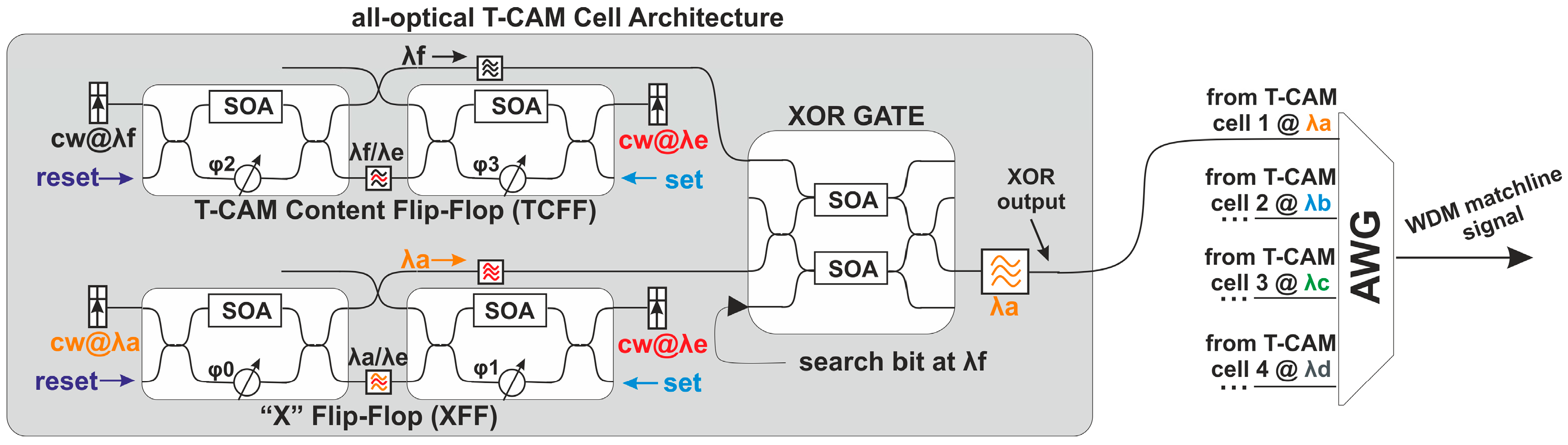
Following the paradigm of optical RAMs, optical alternatives of CAM architectures may facilitate similar advances and speed enhancements towards ultra-fast router AL memories in the high-end router domain. In this regime, some preliminary first steps, stemming from our group, have managed to develop the first photonic alternative CAM-based elements [50,51], which is the main focus of this paper. More specifically, in Section 2, we initially discuss the architectures and main functional building blocks of electronic AL memories, followed by the development of monolithic photonic integration for optical FFs and RAM memories on a monolithic InP platform [33,39] in Section 3. In Section 4, we present the first experimental proof-of-principle of an all-optical Binary CAM (B-CAM) cell architecture at 10 Gb/s [50]. This architecture is later extended in a more advanced all-optical (T-CAM configuration in Section 4, directly supporting, for the first time, a wildcard bit operation of a logical “X” value in the optical domain [51]. By introducing Wavelength encoding in the search word, a 4-bit Matchline (ML) architecture is developed, capable of providing a unique identifying signal upon a match of the destination address with the stored prefix-entry [
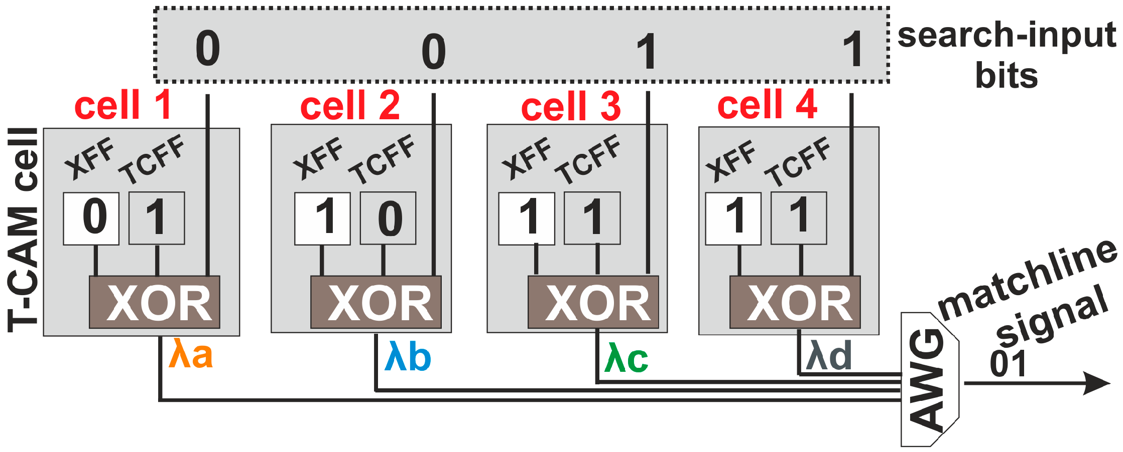
51]. Finally, we present a discussion on the future challenges that need to be addressed for migrating towards optical AL table architectures, bearing promises to directly resolve the AL in the optical domain that can significantly speed-up AL-speeds in high-end router architectures.

2. Electronic Address Look-Up Memory Architectures

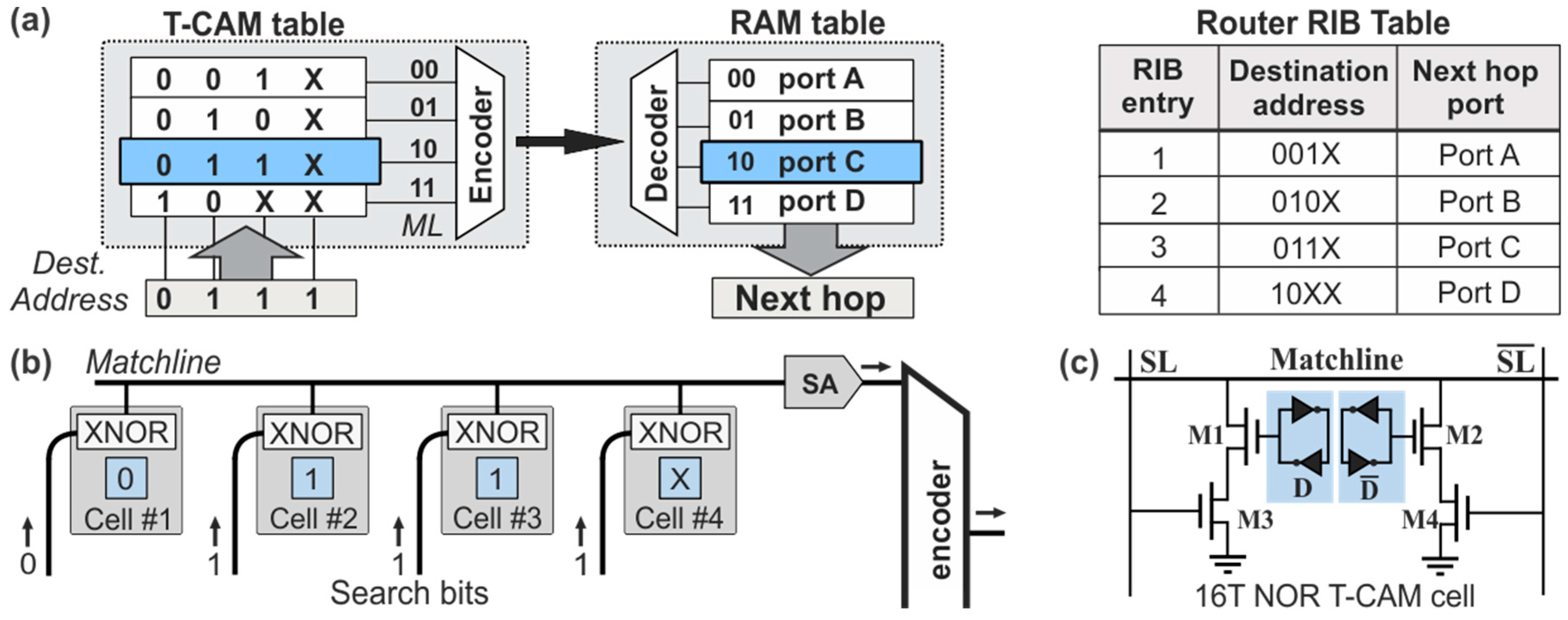
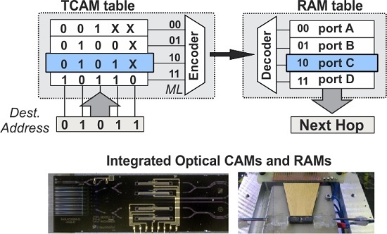
Internet routers forward the data packets of an incoming port to an outgoing port based on an AL comparison function of the destination address of the header. To achieve this, they are equipped with a hardware look-up table that maintains the RIB-list of the destination addresses and their associated outgoing ports for next-hop routing, as depicted in the AL memory table architecture of Figure 1a. The architecture comprises a two dimensional CAM table inter-connected to a two dimensional RAM table. The CAM table stores the prefix-list with the destination addresses, while the RAM table maintains the outgoing port. Each entry of the RIB prefix-list is stored in a mutli-bit memory line, widely known as CAM ML. Upon the arrival of a packet, the header containing the destination address bits is broadcasted to all MLs of the CAM table, where it gets bitwise compared with the contents of the CAM cells. When the stored word of a specific ML matches the incoming search bits of the destination address, a match-signal is generated at the output of the ML, activating the specific line; otherwise, the CAM ML is not enabled. The activated CAM ML can then be mapped though the intermediate encoder-decoder network to the associated RAM table line, where the next-hop routing information is stored, so as to retrieve the outgoing port of the data packet. An example operation of the AL table is described by the RIB table shown at the right side of Figure 1a, assuming an incoming packet designated with a destination address [0111] and an RIB-list with four entries, namely [001X], [010X], [011X], and [10XX]. By broadcasting and bit-wise comparing the destination address with all the RIB-entries, the third prefix of [011X] matches the packet’s destination address. This matching will in turn activate the third line of the RAM forwarding table where port C is stored, indicating the next hop to which the incoming packet has to be forwarded.
A more detailed view of the block diagram describing the logical circuit operation of the 1 × 4 ML is shown in Figure 1b, comprising four parallel CAM cells. The CAM cells have their outputs combined at an inline Sense Amplifier (SA) and are then inter-connected to the encoder/decoder network for communication with the RAM table. Every CAM cell stores a bit of a RIB prefix entry and bears a logical XNOR gate for comparison with the incoming search bits of the destination address. If the search bit and the stored bit are equal, the logic XNOR gate transmits a signal of logic “1” value to the end of the respective ML. Equivalently, when all CAM cells of the line provide a logical match, the SA identifies the exact word match with the stored content and emits a proper signal towards the encoder. On the contrary, when there is a mismatch at any of the bits of the ML, the XNOR gate of the CAM cell provides a logical “0” value at the output, and de-activates the SA and the ML, denoting that a mismatch between the incoming destination address and the stored prefix has occurred. At this point, it is worth noting that MLs consist of Ternary T-CAM cells, in order to support ternary features with masked wildcard bits of “logical X”, as used in subnet masks, rather than simpler Binary CAM cells that store only bits of logical “1” or “0”.
The conventional architecture of the most typical 16T NOR-based electronic T-CAM cell is illustrated in Figure 1c [10], comprising two D-type flip-flops operating as storage cells and marked with a blue highlight. The first memory cell is responsible for storing the actual data-bit [0 or 1] and the second one stores the ternary state information for the “Care” or “Don’t Care” state of the logical “X” value. Each memory cell is typically built on the configuration of two cross-coupled inverters, similar to 6T RAM cells [11], while another two pairs of transistors, (M1, M3) and (M2, M4), form short–circuits to the ground. This configuration ensures that at least one pulldown path from the ML down to the ground exists at any time during a mismatch between the search word and the stored data. On the contrary, a match between the search word bit and the stored data disables both pulldown paths, disconnecting the ML from the ground and feeding its output to the SA. If this matching happens for all the cells of the ML, a NOR logic operation between all CAM outputs, performed at the SA, identifies the exact match of the packet’s destination address with the certain RIB prefix entry.

3. Monolithic Photonic Integration for Optical Memories

To this end, photonic integration processes have matured to the point where a wealth of optical FF and RAM memory configurations have been successfully demonstrated [33,34,35,36,37,38,39,40,41], with most of these demonstrations relying on the mature SOA switching technology, owing to its high-gain, high-speed, and high-yield performance characteristics [
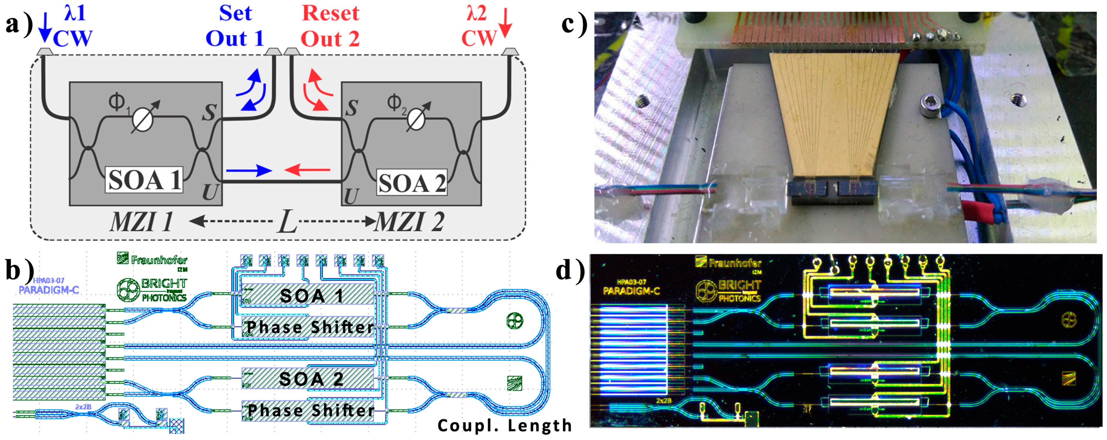
2]. In this paper, our analysis draws from the architecture of an FF memory with two cross-coupled asymmetric SOA-MZI switches, as illustrated in Figure 2a, which was initially developed in [37] and more recently theoretically investigated in the time and frequency domain in [43]. Each SOA-MZI switch features one SOA (SOA1 and SOA2) at the lower branch and a phase shifting element (Φ1 and Φ2) at the upper branch for controlling the biasing conditions of the interferometer. The two SOA-MZIs (SOA-MZI1 and SOA-MZI2) are each powered by a weak Continuous Wavelength (CW) input signal at wavelengths λ1 and λ2, respectively, while their Unswitched output ports (U-ports) are interconnected through a common coupling waveguide path. This symmetric configuration of the two SOA-MZI switches allows for a master-slave operation with the U-output of the master switch controlling the operating condition of the opposite slave switch and blocking its transmission at the U-port. Owing to the symmetric configuration, the roles of the master and slave switch are interchangeable, allowing the FF state to be defined by the wavelength of the emitted signal outputs at either one of the Switched ports (S-ports). The FF state can be monitored through the respective FFOut1 and FFOut2 output ports in terms of high power levels of λ1 and λ2 optical signals, respectively.
The state of the FF can be optically controlled by external Set/Reset (SR) pulses fed through the S-ports of the SOA-MZIs. When a high Set or Reset pulse is injected at the master SOA-MZI, it will block its light-transmission and set it in the slave condition regardless of the previous state of the FF, allowing for the opposite SOA-MZI to recover and become the master. In this arrangement, the two logical values of the data-bit stored in the FF-memory, logical “1” and “0”, can be associated with the high optical power of the wavelength-signal emerging at the two outputs. The present FF memory configuration was initially demonstrated as a hybridly integrated module in [37] with the use of silica-on-silicon integration technology, exhibiting a total footprint of 45 × 12 mm2 and coupling length between the two SOAs of 2.5 cm, which was theoretically shown to be the main speed determining factor of the memory architecture [42,43].
Following the conclusions drawn by the underlying theory on the critical performance parameters [42,43], an integrated version of the SR FF was presented using library-based components of a generic monolithic InP platform [33], to benefit from an integration technique that offers the possibility to fabricate multiple active and passive photonic components on a single chip at a close proximity. The two SOA-MZI switches were fitted in a die footprint-area of 6 × 2 mm2 and cross-coupled together through a 5 mm-long coupling waveguide. In this configuration, the intra FF coupling waveguide was 5 mm-long, reducing the total footprint by two orders of magnitude, compared to the previous hybridly-integrated FF implementation [37]. The mask file of the Photonic Integrated Chip (PIC) is illustrated in Figure 2b. The input MMI couplers of the asymmetric MZIs featured a cross/through coupling ratio of 70/30, with respect to the SOA elements, and the MMIs between the two SOA-MZIs featured a coupling ratio of 50/50. The two SOAs featured an active length of 1 mm, while the biasing of the SOA-MZIs was achieved through the respective current injection phase shifters. Electrical routing of the metal wires connected the anodes and cathodes of the SOAs and the phase shifters to 100 × 100 μm2 pads at the upper edge of the chip. The chip featured an array of eight zero-angled Spot Size Converters (SSC) with a pitch of 127 μm for optical I/O connectivity.
The monolithic InP FF-chip was fabricated by Fraunhofer Heinrich-Hertz-Institut (HHI) within a Multi-Project Wafer (MPW) run of the PARADIGM project funded by the European Commission and was later fully packaged in terms of the optical and electrical contacts for system level characterization. The chip was mounted on top of a ceramic sub-mount module, equipped with a thermistor and a Peltier element for temperature stability, while an 8-I/O fiber array was permanently glued to the I/O left facet of the chip. The metal pads of the chip were wire-bonded to the gold-plated ceramic mount, through gold wires, which also facilitated further connectivity with a Printed Circuit Board (PCB), where a 26-pin D-connector was mounted. The fully-packaged chip can be seen in Figure 2c and a microscope image of the PIC is shown in Figure 2d. The FF device was fully characterized in terms of its active components, i.e., the SOAs and the phase shifters, and was used to experimentally demonstrate a successful Set-Reset FF operation at 10 Gb/s [33], highlighting the potential to store and write data directly in the optical domain.
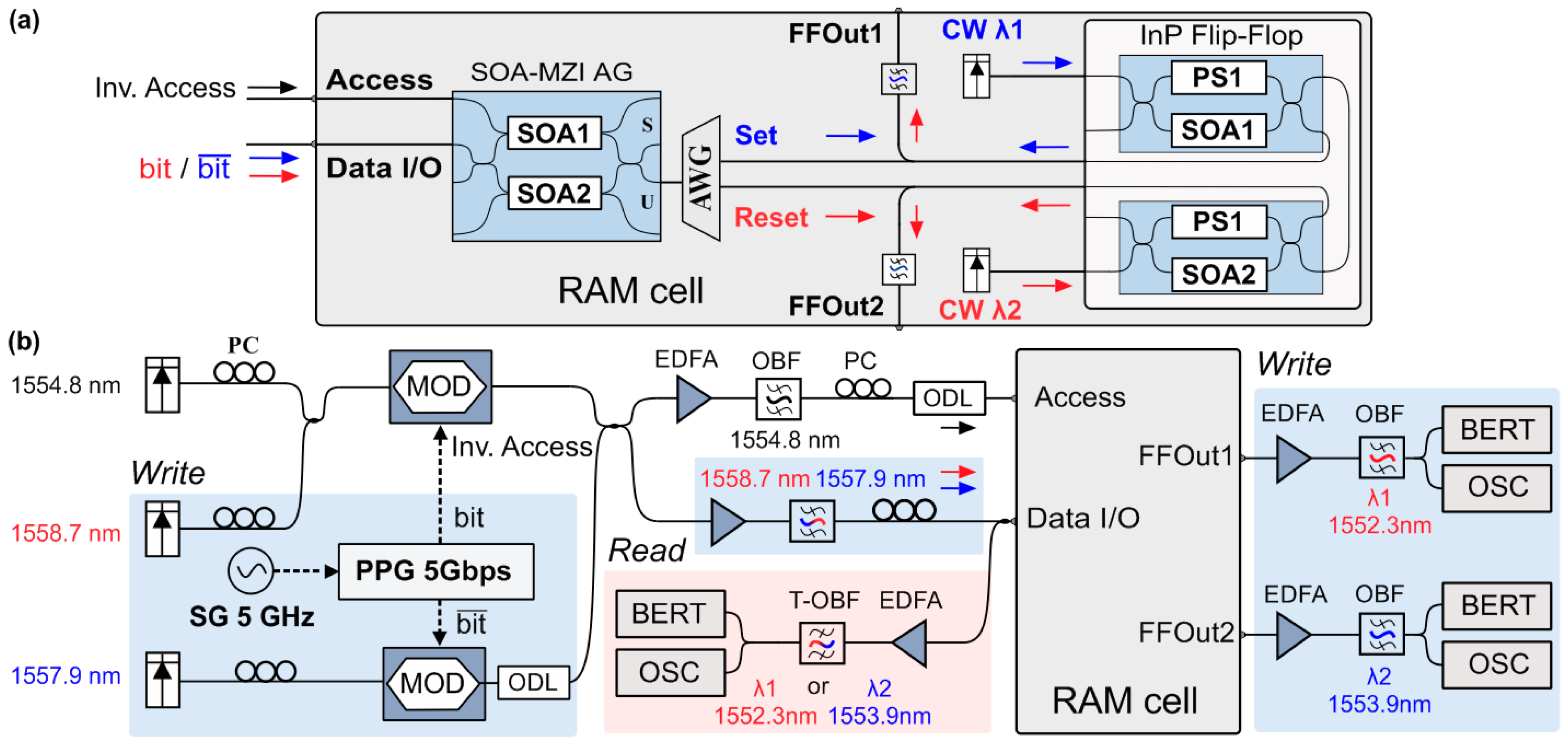
The present monolithic FF architecture served as the memory element of a more complex optical RAM cell configuration, capable delivering Read/Write and Block Access operations. To achieve this, the optical FF is combined with an SOA-MZI optical Access Gate (AG) in a cascade configuration, as shown in Figure 3a. The AG is responsible for granting access to the RAM cell by allowing the data to be either written to or read from the FF each time. The input Data signals are connected to the input of the SOA-MZI AG, and subsequently to an Arrayed Waveguide Grating (AWG) demultiplexer that drives each wavelength to the input/output ports of the FF-memory. The control signal is fed to the upper branch of the SOA-MZI AG, to induce Cross-Phase Modulation (XPM) phenomena. This allows the bit and b i t ¯ signals to pass through the AG switch and emerge at the U-port, when there is no control pulse present, or at the S-port when a control pulse is present. RAM cell operations are then defined based on the values of the logic pulses of the Inverted Access signal and the bit and b i t ¯ signals, which are fed to the RAM I/O Data port and Access port.
During the Write operation, when access is granted to the memory, the complementary bit and b i t ¯ signals carry the incoming data word wavelength encoded on two different wavelengths, while the Inverted Access signal features a logical “0” pulse. Then, the external bit and b i t ¯ signals pass through the AG U-port, and propagate towards the right side, where they are demultiplexed through the AWG and fed to the two inputs of the FF, acting as Set and Reset signals. During the Read operation, the Inverted Access signal again features a logical “0” pulse, while no external data are transmitted to the RAM cell. In this case, the complementary FF output signals, propagating from the FF towards the AG on the left side, are multiplexed in the AWG and fed to the AG through the U-port, so as to emerge at the output of the RAM cell. When access to the memory is blocked, the Inverted Access signal features a logical “1” pulse, which enters the SOA-MZI AG as the control signal, switching the complementary data signals to the S-port and blocking communication with the outer world, allowing for the FF-memory to retain its logic state and memory content.
The experimental setup used to evaluate the complete RAM functionalities is illustrated in Figure 3b. A signal generator (SG) was used to drive a Programmable Pattern generator (PPG) at 5 GHz. The PPG drives two Ti: LiNbO3 modulators using complementary bit-patterns in order to produce 5 Gb/s 27 − 1 Pseudorandom Binary Sequences (PRBS) Non-Return-to-Zero (NRZ) signals. One modulator is responsible for producing the Inverted Access signal at 1554.8 nm and the bit signal at 1558.7 nm, and the other is used for the   b i t ¯ signal at 1557.9 nm. For the evaluation of the Write operation, the three signals were coupled together to form the complementary bit and b i t ¯ pair and one access signal, while the two coupler outputs were amplified using erbium-doped fiber amplifiers (EDFA). The first branch incorporated a 0.6 nm 3 dB-bandwidth Optical Bandpass Filter (OBF) centered at 1554.8 nm to properly filter the Inverted Access signal, while the second branch incorporated a 1 nm 3 dB-bandwidth OBF centered at 1558.3 nm, to filter the bit and b i t ¯ pair. The AWG used has a 0.65 nm 3-dB channel bandwidth. The stored logical value of the FF and the Set/Reset signals could be monitored through the auxiliary ports FFOut1 and FFOut2 at any time of the experiment, which were amplified in respective EDFAs and filtered by suitable Optical Bandpass Filters (OBPFs), before being analyzed by a digital Optical Sampling Oscilloscope (OSC) and Bit Error Rate Tester (BERT). The blue-highlighted areas of the setup were only used during the evaluation of the Write operation, while the red-highlighted part of the setup was only used during the evaluation of the Read operation. To evaluate the READ operation, the FF was set to one of its logic memory states each time by properly adjusting the external CW signal power-levels, meaning that either only λ1 or λ2 was the dominant wavelength of the FF, providing a high FF output power level at either the FFOut1 or FFOut2 port, respectively. A monitor branch was connected at the Data I/O port of the RAM cell comprising an EDFA as a preamplifier and a 0.6 nm 3 dB-bandwidth Tunable OBPF (T-OBPF) that can be tuned at either one or two in order to evaluate one of the two wavelengths. Polarization controllers (PC) were used at several stages of the setup to control signal polarization. Variable optical attenuators (VOA) were also used to properly adjust the power levels of the optical signals, while optical delay lines (ODLs) were employed to ensure signal decorrelation and bit-level synchronization among the signals.
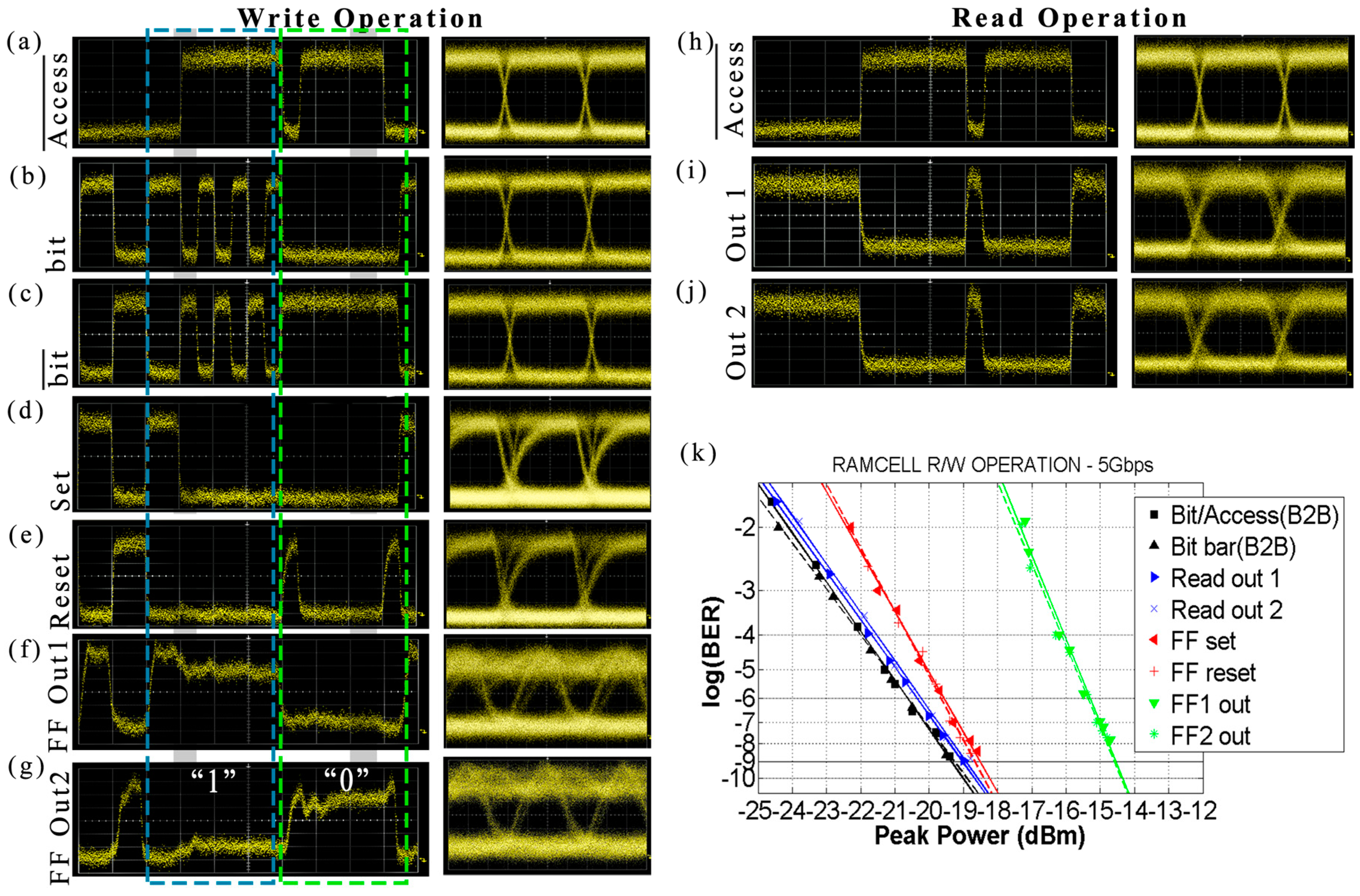
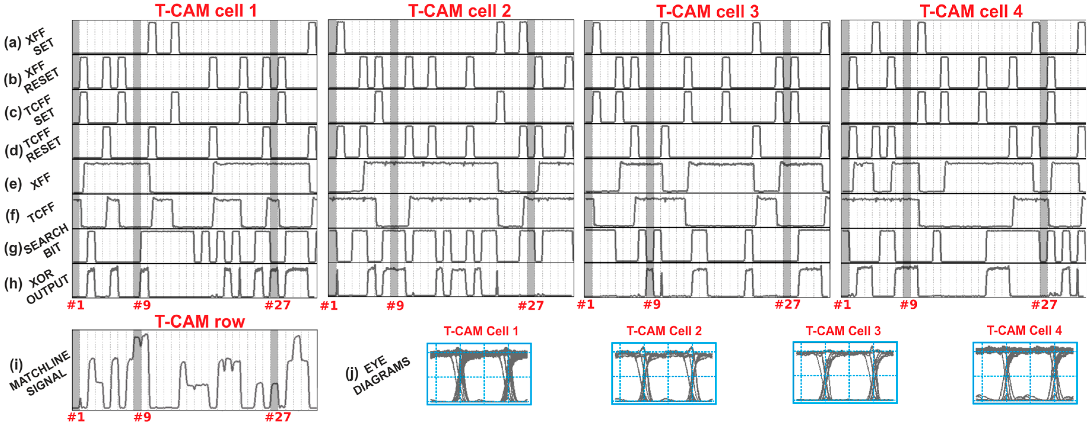
The experimental results obtained from the 5 Gb/s operation can be seen in Figure 4. Figure 4a–g depict synchronized time traces/eye diagrams of the Write operation. Figure 4a shows the Inverted Access signal and Figure 4b,c show the bit and b i t ¯ signals that were launched in the RAM cell, respectively. Figure 4d,e illustrate the Set/Reset signals originating from the incoming bit and b i t ¯ signals, after the access-controlling operation of the AG, where it is clear that they only imprint the logical “1bit and b i t ¯ pulses, respectively, when there is no logical “1” pulse at the Inverted Access signal. The proof-of-principle of the Write operation is then verified by monitoring the FF stored content through the signals emerging at the respective FFOut1 and FFOut2 ports in Figure 4f,g, where it can be seen that the FF changes its logic state when there is an incoming Set or Reset pulse and maintains its state until the next Set/Reset pulse arrival. The eye diagrams of the FF output signals feature a recovery time of 150 ps and an Extinction Ratio (ER) of 6 dB.
Figure 4h–j depict synchronized time traces and the respective eye diagrams for the Read operation. For this evaluation, the FF was set to one logic state and the data were then read by transmitting the Inverted Access signal, shown in Figure 4h. Figure 4i,j illustrate the time traces of the RAM cell output signals, after the random access controlling operation of the AG for both of the FF logic states. A high output value is only obtained when there is no Inverted Access signal pulse present, indicating that access is granted for the Read operation, while when there is a high optical power for the Inverted Access signal, the RAM output of the RAM cell features a logical “0” and access to the memory is thus blocked. The eye diagram of the read output features an ER of 9 dB.
Figure 4k shows the BER measurements obtained for both the Write and Read RAM cell functionalities, where, in all cases, error free operations are demonstrated. For the Write operation, the BER diagrams reveal a power penalty of 0.6 dB for the Set and Reset signals compared to the Back-to-Back measurements of the bit and b i t ¯ signals, and in turn, 4.6 dB for the FFOut1 and FFOut2 signals of the data written to the RAM cell, while for the case of the Read operation, a power penalty of only 0.5 dB was obtained at the 10−9 condition. The results were obtained with a current injection of around 250 mA for each SOA, while when relying on four SOAs operating at 5 Gb/s, the resulting energy efficiency per bit is 400 pJ/bit.

4. Optical CAM Technology

In this section, we describe the recent developments towards developing optical CAM architectures, spanning from the first optical Binary CAM cell to a T-CAM cell layout and the design of multi-bit CAM ML architectures.

4.1. Experimental Demonstration of an Optical CAM Cell

The architecture of the optical Binary CAM cell is schematically illustrated in Figure 5a, comprising the optical FF memory connected to an SOA-MZI XOR logic gate. The optical FF stores the data of the CAM cell, while the XOR logic gate is used for comparing the incoming search bit of the destination address with the stored bit of the prefix. As described previously, the FF is powered by two wavelengths, λ1 and λ2, which are emitted at its two outputs, respectively. In order to achieve a content Comparison operation, one of the two wavelengths, carrying the stored bit information, here λ1, is connected as the control signal to the SOA-MZI XOR gate, while the second control branch of the SOA-MZI is fed with the incoming search bit. The comparison result between the search bit and the FF-memory content is imprinted on a new wavelength, λ3, that is fed as a CW probe signal at the SOA-MZI gate and emerges at its S-output port, forming the final CAM cell output signal. When the two signals feature equal bit-pulses and a match occurs between them, the λ3-CW emerges at the U port of the SOA-MZI and a bit pulse of logical “0” is thus obtained at the S-port and the CAM cell output. On the contrary, when the search bit does not match the FF memory content, a differential π-phase shift is obtained at the SOA-MZI, and the λ3-CW signal emerges at the S-port and a pulse of logical “1” is obtained at the CAM cell output. Regarding the update of the CAM memory content, a Write operation has to be performed for the FF by launching Set/Reset pulses through the respective CAM cell optical ports, so as to change its logic state.
The proposed optical CAM cell architecture was experimentally investigated for both operations, i.e., content Comparison and Write operation at 10 Gb/s, using the experimental setup shown in Figure 5b. For the Comparison operation, the red-highlighted area of the setup was used. A 10 GHz SG was used to drive a PPG that modulated a LiNbO3 modulator, in order to produce the 10 Gb/s NRZ 27 − 1 PRBS signal at a λ4 = 1557.9 nm wavelength, forming the search signal that is transmitted to the SOA-MZI XOR gate as the control signal and thus emulating the external search-bit. The comparison result is imprinted at the λ3 = 1548 nm wavelength and the result is obtained at the respective SOA-MZI XOR output, after being filtered at a 0.6 nm 3 dB-bandwidth OBPF. For the Write operation, the blue-highlighted area of the setup was used. The 10 GHz SG was connected to a PPG, which then provided two 10 Gb/s NRZ data streams that modulated two LiNbO3 modulators to generate the Set/Reset data steams at a 1558.7 nm wavelength. The logic state of the FF was recorded through the respective FFOut1/2 ports at λ1 and λ2, respectively, filtered by 0.6 nm 3 dB-bandwidth OBPFs centered at λ1 and λ2, which were then analyzed by an OSC and a BERT. EDFAs and VOAs were incorporated in both experimental setups for power loss compensation and power level management of the signals, while PCs were used to adjust the signal polarization states.
The experimental results obtained in the optical CAM cell demonstration can be seen in Figure 6. Figure 6a–d show the time traces and the respective eye diagrams obtained during the Content Comparison operation. The FF was manually set each time to one of the two states and studied for both stored FF data-bit of logical “0” and logical “1”, shown in Figure 6a. For the first logic state, when the FF holds a logic value of “0”, CW1 emerges at FFOut1 with a low power level and enters the SOA-MZI XOR gate, while Figure 6b shows the time trace of the search bit signal acting as the second control signal of the XOR operation. Figure 6c shows the result of the XOR comparison, where it can be seen that a logic “1” pulse is only obtained when a “logic 1” pulse is present at the search bit, featuring the same data pattern and confirming an XOR operation with the FF state of logic “0”. Equivalently, when the FF holds a logic value of “1”, as shown in the second column of Figure 6a, and is compared with the input search bit trace, the obtained CAM cell output features an inverse logic bit pattern compared to the input search bit, as shown in Figure 6c, verifying the XOR proof-of-principle. The eye diagrams of the obtained XOR output signals of the CAM cell are shown in Figure 6d, featuring an average ER of 9.2 dB.
The results for the CAM cell Write mode functionality are presented in Figure 6e–h. Figure 6e,f show the Set and Reset signals and their corresponding eye diagrams, that were sent to the CAM cell in order to control the state of the FF. Figure 6g,h show the two stored bit values of the FF as a recorder at its two outputs, where it can be seen that the FF changes state upon the arrival of a Set (or Reset) pulse with a recovery time of 80 ps and the memory is then maintained until the arrival of the next opposite pulse. The two FF output signals clearly feature open eye diagrams, revealing an average ER of 6.5 dB. The two operations of the CAM cell were also evaluated with the aid of BER measurements and the results are shown in Figure 6i,j for the content comparison and the write functionality, respectively. An error free operation was achieved at the 10−9 operating condition for both states of the FF and for both CAM cell functionalities. The BER diagram in Figure 6i reveals a successful content comparison at 10 Gb/s with a power penalty of 1 dB, associated mainly with the signal degradation induced by the optical XOR gate, while the BER diagram of Figure 6j for the Write functionality exhibits a power penalty of 4 dB, owing to the dynamic operation of the FF. For the CAM cell experimental demonstration, the four SOAs were again operated at a current of 250 mA each, leading to an energy efficiency of 200 pJ/bit at a 10 Gb/s operational speed.

4.2. Ternary CAM Cell and Matchline Architecture

In this section, we move from the all-optical B-CAM cell to the presentation of the all-optical T-CAM cell architecture and its interconnection in an all-optical T-CAM row arrangement targeted for use in AL tables such as the one presented in Figure 1a, enabling the essential subnet-masked operation needed in modern router applications. The proposed optical T-CAM cell architecture comprises two optical FFs and an optical XOR gate; the 1st FF is used for storing the actual T-CAM cell contents and the 2nd FF for implementing the “X” state support. The XOR gate, on the other hand, enables the T-CAM cell search capability. Moving to the complete row arrangement, the proposed all-optical T-CAM row architecture comprises an indicative number of four T-CAM cells followed by a novel WDM-encoded ML design, providing a comparison operation for complete 4-bit optical words. In order to achieve this, an AWG is utilized to multiplex all the T-CAM cell XOR outputs in a common multi-wavelength row output signal that determines whether a success comparison result is achieved throughout the complete T-CAM row.
Figure 7 presents the proposed all-optical T-CAM cell consisting of two FF modules and one XOR gate. The XOR gate is necessary for realizing the comparison operation between the search-bit and the value stored in the T-CAM cell. The lower FF is named XFF and is necessary for implementing the third state “X”, while the upper FF is named T-CAM Content FF (TCFF) and stores the actual content that can be either a logical “0” or “1”. When a subnet-masked operation is desired, the XFF’s content equals 0, implying that the TCFF respective content has to be ignored. As such, the respective XOR operation does not take into account the TCFF content and the comparison result is equal to a logical “0”, independently of the value of the search-bit. On the contrary, in the case where the TCFF value has to be taken into account, the XFF content is equal to a logical “1” and the XOR output depends upon the comparison between the TCFF value and the respective search-bit.
For both FFs, the previously described Set/Reset pulse mechanism is used in order to switch between the two possible logical states. The XFF and TCFF are each powered by two CW laser beams: λe is used as the input signal at the right-side switches of both XFF and TCFF, while a CW signal at λa and λf is launched as the input signal at the left-side SOA-MZI switches of the XFF and TCFF, respectively. As such, the content of the XFF and the TCFF gets encoded on λa and λf wavelengths as the FF output signals, respectively. The XFF output signal is then fed as the input signal at the XOR gate, after being filtered in an OBF. On the other side, the TCFF output at λf enters the XOR gate as the control signal of the upper-branch SOA. The lower branch SOA of the XOR gate is being fed with the input search bit that acts as the second control signal. In this way, the TCFF output and search bit values get logically XORed and the comparison result gets imprinted on the XFF output signal at λa, which is used as the XOR input. Whenever the T-CAM cell is in the “X” state, the XFF output is equal to a logical “0”, resulting in a logical “0” at the final XOR output, irrespective of the TCFF and search bit values. On the contrary, the final XOR output depends on the comparison result between the TCFF output and search bit values when the XFF output equals a logical “1”: when both the TCFF output and search bit signals have the same value, the XOR output is “0”, while in the opposite case, i.e., when they have different values, the XOR output equals “1” and is imprinted on the XFF output at λa.
By assigning a different wavelength for carrying the optical XOR output at every individual T-CAM cell within a row, all four of the T-CAM cell outputs can be combined at the row output by using an AWG multiplexer, as presented at the right side of Figure 7; λa through λd are used for the different cell outputs, while λe, λf, and the wavelengths used for the Set/Reset signals are employed in all T-CAM cells. This leads to a WDM-encoding scheme that produces the corresponding ML signal at the final row output. In this way, an ML signal of a logical value “0” indicates a completely matched comparison result since all the individual XOR outputs will be equal to a logical “0”. On the contrary, a non-zero optical power level obtained at the encoder input indicates that at least one individual XOR output produces a comparison miss, denoting a non-completely matched row. A more generic representation of the proposed T-CAM row architecture is presented in Figure 8.
Figure 9 presents the simulation results of the T-CAM row architecture for both Search and Write operations and at a line-rate of 10 Gb/s. The simulation models have been developed using the VPI Photonics suite and both the XOR gate and FF models are based on experimentally verified building blocks. The SOA model used in both the XOR gates and FFs is identical to the one presented and experimentally validated in [52]. The wavelengths used in the four-cell arrangement of Figure 7 are equal to: λa: 1564.19 nm, λb: 1562.56 nm, λc: 1559.31 nm, λd: 1557.36 nm, λe: 1554.78 nm, λf: 1546.12 nm, Set: 1548.35 nm, and Reset: 1551.88 nm.
Figure 9a,b illustrate the Set/Reset pulse traces that are fed into the XFFs and determine whether the XFF has to define an “X” state for the T-CAM cell. Figure 9c,d illustrate the Set/Reset pulse traces that are fed into the TCFFs of the four cells dictating the logical content of every TCFF. Figure 9e depicts the XFF output signal, while Figure 9f illustrates the TCFF content transitions for every T-CAM cell. As can be seen in both Figure 9e,f, a successful bit storage operation is achieved according to the respective Set/Reset pulse traces; the presence of a Set pulse leads to an FF content transition to the 0 logical state, while the presence of a Reset pulse leads to an FF content transition to the logical state of 1. Figure 9g presents the search-bit pulse traces that are fed into the XOR gates of the four T-CAM cells as parallel streams in order to be compared with the respective T-CAM cell contents. The search-bit pulse traces are NRZ 27 − 1 PRBS at a line-rate of 10 Gb/s. Figure 9h shows the XOR output signals that also form the T-CAM cell outputs and Figure 9i illustrates the power level of the final ML signal that is produced at the row output and just after the AWG multiplexer. As can be noticed, this is a multilevel signal, with every different power level corresponding to a different number of bit-level search misses. When all T-CAM cells match the four bits of the incoming search-input signal, no optical power is recorded at the AWG output.
A successful ML operation of the complete T-CAM row can be verified for the entire pulse traces used as the four parallel search bit sequences. Three representative examples at the timeslots #1, #9, and #27 have been highlighted in order to facilitate the understanding of the T-CAM row performance in different situations. In the example of timeslot #1, all four T-CAM cells are in the “X” state since all respective XFF outputs are equal to “0”, which finally results in an XOR output of “0”, regardless of the TCFF and search-bit values. As expected, the final ML signal at timeslot #1 is also equal to “0”, corresponding to a complete match between the T-CAM row and the search-input contents. Within timeslot #9, none of the T-CAM cells are in the “X” state since all XFF outputs are equal to a logical 1. For T-CAM cell #1, the XOR output is equal to a logical “0” since the TCFF and the search-bit content are equal. However, for the remaining three T-CAM cells, the respective XOR outputs are equal to a logical “1”, denoting the different content between the corresponding TCFF and search-bit signals. The presence of three optical pulses at different wavelengths but within the same timeslot #9 designates that the optical power obtained at the AWG output will equal the sum of the power levels of the three individual pulses, obviously leading to an ML signal with non-zero power that indicates a non-perfectly matched search operation. In the example of timeslot #27, T-CAM cells #2 and #4 are in the “X” state since their XFF content equals a logical “0”. As such, the respective XOR outputs are also equal to “0” and this happens even in the case of T-CAM cell #4, where the TCFF content and its respective search-bit are different. Regarding cell #3, the XOR output equals “0” because both the TCFF content and the search-bit are equal. However, cell #1 has an XOR output of “1” since TCFF content and the respective search-bit have different values. This single optical pulse obtained as the result of the comparison along the entire T-CAM row is then also translated into a non-zero power level at the AWG output, again suggesting a non-matched row, while Figure 9j presents clearly open eyes for all four T-CAM cells with an ER of 13 dB. The energy efficiency of the TCAM cell is 300 pJ/bit.

5. Future Challenges and Discussion

The presented multi-wavelength optical subsystems provide the necessary constituents for synthesizing a new design roadmap for a photonic AL memory architecture that can reap the unique benefits of a high-bandwidth and low-power consumption offered by optical technology. The use of discrete SOA-MZIs interconnected to fiber-pigtailed monolithic integrated FF-devices allows us to overcome the critical speed determining factor of the large intra-FF coupling distance [42,43] and facilitates the full characterization of each RAM cell and CAM cell independently, without any speed limitation, when unidirectional data-communication is employed. However, the latency of the fiber-network of the complete optical ML architecture introduces some latency in the overall destination address resolution, when the content comparison output of the CAM cell has to be propagated to the RAM cell for a Read operation. By reaping the benefits of mature photonic integration multiple photonic components per chip [2], a fully integrated Matchline could enable studying all RAM and CAM functionalities simultaneously, with a shorter latency for the destination address resolution operation, which could be further improved by incorporating gain-accelerating techniques [53]. Meanwhile, for a simultaneous synchronous write operation at the RAM cell and CAM cell of the envisioned optical ML, the write operation should be performed at 5 Gb/s due to the cascaded switching operation at the AG, which is already an order of magnitude faster than the respective electronic memory speed [6,54], while faster memory updates and network changes are subject to the use of higher speed SOAs. Drawing from our presented initial experimental timing tests with short rise/fall times of 90 ps, optical CAM memories can also significantly reduce the reconfiguration times towards enabling rapid updates of the RIB-memory.
Our proposed scheme has relied on power-hungry 1 mm-long SOAs of a generic foundry that necessitate external currents of 250 mA and a power consumption of 0.5 W for each SOA for proof-of-concept demonstration purposes, resulting in an optical multi-bit multi-wavelength ML architecture with a power efficiency of 300 pJ/bit per clock cycle when operating at 10 Gb/s. This value can be reduced by orders of magnitudes when shifting to more sophisticated low-power III/V-on-SOI photonic crystal technologies with nm-scale dimensions and power consumptions of a few mW [55], towards energy efficiencies of a few fJ/bit, comparable to electronics [6,20,21]. Meanwhile the use of the envisioned high-speed multi-bit optical ML architectures technology provides a possible path towards circumventing the use of power-hungry cost expensive power conversion at SERDES equipment, that can allocate up to half of the power consumption of a low power transceiver [24]. Additional power consumption benefits may also be obtained, when shifting to higher bitrates beyond 10 Gb/s [43] or even when exploiting the wavelength dimension for a single Access Gates shared among the multiplexed outputs of multiple optical RAMs [45].
The use of optical AL memories can also benefit from the inherent support of WDM techniques for enhancing wavelength parallelism and reaping the advantages of a new multiplexing capability that is so far not feasible in electronic AL memories. Towards a more practical application of a fully integrated optical ML architecture suitable for handling IPv4 addresses, and considering the typical table sizes of electronic memories with 4K entries [56], a row-capacity of 32-bit would be required, while for compatibility with next generation IPv6 addresses, a 128-bit memory would be required. In this case, the ML architecture will utilize 32 or 128 wavelengths, respectively, one per TCAM cell output, similar to the wavelength addressable large-scale photonic integrated photonic memories of 128-bits [30] or the 128-wavelengths of the optically connected RAM architectures for High Performance Computers [57], as well as an AWG with a similarly high channel count [1]. The assignment of different wavelengths at the various T-CAM cells of an ML certainly adds an extra degree of freedom to system-designs for more efficient architectures, especially when considering multiple simultaneous WDM memory schemes with parallel wavelengths written to the T-CAM cells of an ML for fast memory updates. This can be of utter importance with the emergence of SDN and OpenFlow architectures that enforce a dynamic network operation with frequent updates of network topologies and multiple real time changes in the RIB-list [25,26]. Although the SDN controllers are increasingly optimized for swift policy updates, the T-CAM tables remain yet unoptimized for fast updates [27,28], which may trigger hundreds to thousands of table entry-moves and write-memory operations [26]. Measurements on the timings of such AL-table updates have revealed a few hundreds of ms-long response times [25,26,27,28], as AL-updates need to be organized in electronic T-CAM tables with sequential time-multiplexed memory accesses through a memory-bus of a limited bandwidth. In this case, the optical nature of the proposed T-CAM may facilitate wavelength multiplexed memory access schemes in order to perform multiple simultaneous Write operations at 10 Gb/s, either when updating the prefix-list of the optical CAM-table or the outgoing ports stored in the optical RAM table, providing manifold improvements in the AL memory throughput.
When developing programmable low power optical AL-memory architectures, further system benefits could potentially be obtained by the introduction of the programmability of the optical memory content [31] or the use of a non-volatile photonic integrated memory [32]. However, apart from the optimization of the memory cell, additional developments are still required, as, e.g., the development of a proper input WDM interconnect network, capable delivering the input bit in vertical CAM-column arrangements, known as Searchlines, or the intermediate encoder/decoder interconnect network and peripheral sub-circuits that undertake the communication between the CAM-table and the RAM table, potentially taking into account the case of priority encoding, when multiple prefix matches are formed by the use of ternary bits. These next steps could potentially follow similar concepts as the ones suggested by the all-passive wavelength-based Column Address Selector [45], the peripheral circuitry [46], and/or the optical tag comparator [47] of the more detailed studies in the area of optical RAM architectures.

6. Conclusions

A novel WDM optical CAM bank architecture is presented, comprising a list of ML memory architectures capable of performing a content Comparison at 10 Gb/s for fast Address Look-Up (AL) operations. The presented architecture is built on the first optical Binary and Ternary CAM cell architectures, as alternatives to the ubiquitous optical Flip-Flops and optical Random Access Memory (RAM) cells with location-based memory addressing. The proposed ML architecture also reveals the potential for a multi-wavelength operation for the full exploitation of wavelength encoding, paving the way for multiple parallel WDM write access operations, suggesting manifold improvements in the programmability and reconfigurability of AL memories.

Acknowledgments

This work has been supported by the FP7-PEOPLE-2013-IAPP-COMANDER project (Contract No. 612257). The EU-FP7-ICT-PARADIGM project (Contract No. 257210) is acknowledged for the FF chip design and fabrication. The authors would also like to acknowledge Ronald Broeke and Francisco Soares for the chip fabrication and Tolga Tekin for the packaging.

Author Contributions

C.V. and S.P. designed and performed the experiments, P.M. designed and performed the simulations, A.M. and N.P. conceived the initial ideas. C.V., S.P. and P.M. wrote the paper and A.M. and N.P. reviewed the results and the manuscript.

Conflicts of Interest

The authors declare no conflict of interest.

References

  1. The Internet of Things How the Next Evolution of the Internet Is Changing Everything. Available online: http://www.cisco.com/c/dam/en_us/about/ac79/docs/innov/IoT_IBSG_0411FINAL.pdf (accessed on 10 May 2017).
  2. Smit, M.; Leitjens, X.; Ambrosius, H.; Bente, E.; Tol, J.; Smalbrugge, B.; Vries, T.; Geluk, E.J.; Bolk, J.; Veldhoven, R.; et al. An introduction to InP-based generic integration technology. IOP Semicond. Sci. Technol. 2014, 29, 1–41. [Google Scholar] [CrossRef]
  3. Winzer, P. Scaling Optical Fiber Networks: Challenges and Solutions. Opt. Photonics News 2015, 26, 28–35. [Google Scholar] [CrossRef]
  4. Ballani, H.; Francis, P.; Cao, T.; Wang, J. Making routers last longer with ViAggre. In Proceedings of the 6th USENIX Symposium on Networked Systems Design and Implementation, Boston, MA, USA, 22–24 April 2009. [Google Scholar]
  5. Available Pool of Unallocated IPv4 Internet Addresses Now Completely Emptied. Available online: https://www.icann.org/en/system/files/press-materials/release-03feb11-en.pdf (accessed on 10 May 2017).
  6. Nii, K.; Amano, T.; Watanabe, N.; Yamawaki, M.; Yoshinaga, K.; Wada, M.; Hayashi, I. A 28 nm 400 MHz 4-Parallel 1.6 Gsearchs 80 Mb Ternary CAM. In Proceedings of the IEEE International Solid-State Circuits Conference, San Francisco, CA, USA, 9–13 February 2014. [Google Scholar]
  7. Growth of the BGP Table—1994 to Present. Available online: http://bgp.potaroo.net/ (accessed on 10 May 2017).
  8. Arianfar, S.; Nikander, P.; Ott, J. On content-centric router design and implications. In Proceedings of the Re-Architecting the Internet Workshop, Philadelphia, PA, USA, 30 November 2010. [Google Scholar]
  9. Ruiz-Sanchez, M.A.; Biersack, E.W.; Dabbus, W. Survey and Taxonomy of IP Address Lookup Algorithms. IEEE Netw. 2001, 15, 8–23. [Google Scholar] [CrossRef]
  10. Pagiamtzis, K.; Sheikholeslami, A. Content-addressable memory (CAM) circuits and architectures: A tutorial and survey. IEEE J. Solid State Circuits 2006, 41, 712–727. [Google Scholar] [CrossRef]
  11. Athe, P.; Dasgupta, S. A comparative study of 6T, 8T and 9T decanano SRAM cell. In Proceedings of the IEEE Symposium on Industrial Electronics & Applications, Kuala Lumpur, Malaysia, 4–6 October 2009. [Google Scholar]
  12. Chisvin, L.; Duckworth, R.J. Content-Addressable and Associative Memory: Alternatives to the Ubiquitous RAM. Computer 2002, 22, 51–64. [Google Scholar] [CrossRef]
  13. Shah, D.; Gupta, P. Fast Updating Algorithms for TCAMs. IEEE Micro 2001, 21, 36–47. [Google Scholar] [CrossRef]
  14. Yang, B.D.; Kim, L.S. A Low-Power CAM Using Pulsed NAND–NOR Match-Line and Charge Recycling Search-Line Driver. IEEE J. Solid State Circuits 2005, 40, 1736–1744. [Google Scholar] [CrossRef]
  15. Yang, B.D.; Lee, Y.K.; Sung, S.W.; Min, J.J.; Oh, J.M.; Kang, H.J. A Low Power Content Addressable Memory Using Low Swing Search Lines. IEEE Trans. Circuits Syst. I 2011, 58, 2849–2858. [Google Scholar] [CrossRef]
  16. Kasai, G.; Takarabe, Y.; Furumi, K.; Yoneda, M. 200 MHz/200 MSPS 3.2 W at 1.5 V Vdd, 9.4 Mbits ternary CAM with new charge injection match detect circuits and bank selection scheme. In Proceedings of the IEEE Custom Integrated Circuits Conference, San Jose, CA, USA, 24–26 September 2003. [Google Scholar]
  17. Hayashi, I.; Amano, T.; Watanabe, N.; Yano, Y.; Kuroda, Y.; Shirata, M.; Dosaka, K.; Nii, K.; Noda, H.; Kawai, H. A 250-MHz 18-Mb Full Ternary CAM with Low-Voltage Matchline Sensing Scheme in 65-nm CMOS. IEEE J. Solid State Circuits 2013, 48, 2671–2680. [Google Scholar] [CrossRef]
  18. Moradi, M.; Qian, F.; Xu, Q.; Mao, Z.M.; Bethea, D.; Reiter, M.K. Caesar High Speed and Memory Efficient Forwarding Engine for Future Internet Architecture. In Proceedings of the ACM/IEEE Symposium on Architectures for Networking and Communications Systems, Oakland, CA, USA, 7–8 May 2015. [Google Scholar]
  19. Jiang, W.; Wang, Q.; Prasanna, V.K. Beyond TCAMs: An SRAM-Based Parallel Multi-Pipeline Architecture for Terabit IP Lookup. In Proceedings of the IEEE INFOCOM Conference on Computer Communications, Phoenix, AZ, USA, 13–18 April 2008. [Google Scholar]
  20. Jeloka, S.; Akesh, N.B.; Sylvester, D.; Blaauw, D. A 28 nm Configurable Memory TCAM BCAM SRAM Using Push Rule 6T Bit Cell Enabling Logic in Memory. IEEE J. Solid State Circuits 2016, 51, 1009–1021. [Google Scholar] [CrossRef]
  21. Arsovski, I.; Hebig, T.; Dobson, D.; Wistort, R. A 32 nm 0.58-fJ/Bit/Search 1-GHz Ternary Content Addressable Memory Compiler Using Silicon-Aware Early-Predict Late-Correct Sensing With Embedded Deep-Trench Capacitor Noise Mitigation. IEEE J. Solid State Circuits 2013, 48, 932–939. [Google Scholar] [CrossRef]
  22. Kilper, D.C.; Atkinson, G.; Korotky, S.K.; Goyal, S.; Vetter, P.; Suvakovic, D.; Blume, O. Power trends in communication networks. IEEE J. Sel. Top. Quantum Electron. 2011, 17, 275–284. [Google Scholar] [CrossRef]
  23. Tucker, R.S.; Baliga, J.; Ayre, R.; Hinton, K.; Sorin, V.W. Energy Consumption in IP Networks. In Proceedings of the European Conference on Optical Communication, Brussels, Belgium, 21–25 September 2008. [Google Scholar]
  24. Audzevich, Y.; Watts, P.; West, A.; Mujumdar, A.; Crowcroft, J.; Moore, A. Low power optical transceivers for switched interconnect networks. In Proceedings of the International Conference on Advanced Technologies for Communications, Ho Chi Minh City, Vietnam, 16–18 October 2013. [Google Scholar]
  25. Hey, K.; Khalid, J.; Gember-Jacobson, A.; Das, S.; Akella, A.; Erran, L.L.; Thottan, M. Measuring Control Plane Latency in SDN-enabled Switches. In Proceedings of the 1st ACM SIGCOMM Symposium on Software Defined Networking Research, Santa Clara, CA, USA, 17–18 June 2015. [Google Scholar]
  26. Karam, R.; Puri, R.; Ghosh, S.; Bhunia, S. Emerging Trends in Design and Applications of Memory-Based Computing and CAMs. IEEE Proc. 2015, 103, 1311–1330. [Google Scholar] [CrossRef]
  27. Katta, N.; Alipourfard, O.; Rexford, J.; Walker, D. CacheFlow: Dependency-Aware Rule-Caching for Software-Defined Networks. In Proceedings of the Symposium on SDN Research, New York, NY, USA, 14–15 March 2016. [Google Scholar]
  28. Wen, X.; Yang, B.; Chen, Y.; Errann, L.L.; Bu, K.; Zheng, P.; Yang, Y.; Hu, C. RuleTris: Minimizing Rule Update Latency for TCAM-based SDN Switches. In Proceedings of the International Conference on Distributed Computing Systems, Nara, Japan, 27–30 June 2016. [Google Scholar]
  29. Koonen, A.M.J.; Yan, N.; Olmos, J.V.; Monroy, I.T.; Peuchert, C.; Breusegem, E.V.; Zouganeli, E. Label-Controlled Optical Packet Routing-Technologies and Applications. IEEE J. Sel. Top. Quantum Electron. 2007, 13, 1540–1550. [Google Scholar] [CrossRef]
  30. Kuramochi, E.; Nozaki, K.; Shinya, A.; Takeda, K.; Sato, T.; Matsuo, S.; Taniyama, H.; Sumikura, H.; Notomi, M. Large-scale integration of wavelength-addressable all-optical memories on a photonic crystal chip. Nat. Photonics 2014, 8, 474–481. [Google Scholar] [CrossRef]
  31. Song, J.F.; Luo, X.S.; Lim, A.E.J.; Li, C.; Fang, Q.; Liow, T.Y.; Jia, L.X.; Tu, X.G.; Huang, Y.; Zhou, H.F.; et al. Integrated photonics with programmable non-volatile memory. Sci. Rep. 2016, 6. [Google Scholar] [CrossRef] [PubMed]
  32. Rios, C.; Stegmaier, M.; Hosseini, P.; Wang, D.; Scherer, T.; Wright, D.C.; Bhaskaran, H.; Pernice, W.H.P. Integrated all-photonic non-volatile multi-level memory. Nat. Photonics 2015, 9, 725–732. [Google Scholar] [CrossRef]
  33. Pitris, S.; Vagionas, C.; Kanellos, G.T.; Kisacik, R.; Tekin, T.; Broeke, R.; Pleros, N. All-optical SR Flip-Flop based on SOA-MZI switches monolithically integrated on a generic InP platform. In Proceedings of the Smart Photonic and Optoelectronic Integrated Circuits XVIII, San Francisco, CA, USA, 23 May 2016. [Google Scholar]
  34. Vagionas, C.; Fitsios, D.; Kanellos, G.T.; Pleros, N.; Miliou, A. All optical flip flop with two coupled travelling waveguide SOA-XGM switches. In Proceedings of the Conference on Lasers and Electro-Optics, San Jose, CA, USA, 6–11 May 2012. [Google Scholar]
  35. Liu, L.; Kumar, R.; Huybrechts, K.; Spuesens, T.; Roelkens, G.; Geluk, E.J.; Vries, T.; Regrenny, P.; Thourhout, D.V.; Baets, R.; et al. An ultra-small, low-power, all-optical flip-flop memory on a silicon chip. Nat. Photonics 2010, 4, 182–187. [Google Scholar] [CrossRef]
  36. Sakaguchi, J.; Katayam, T.; Kawaguchi, H. High Switching-Speed Operation of Optical Memory Based on Polarization Bistable Vertical-Cavity Surface-Emitting Laser. IEEE J. Quantum Electron. 2010, 46, 1526–1534. [Google Scholar] [CrossRef]
  37. Pleros, N.; Apostolopoulos, D.; Petrantonakis, D.; Stamatiadis, C.; Avramopoulos, H. Optical static RAM cell. IEEE Photonics Technol. Lett. 2009, 21, 73–75. [Google Scholar] [CrossRef]
  38. Vagionas, C.; Fitsios, D.; Kanellos, G.T.; Pleros, N.; Miliou, A. Optical RAM and Flip-Flops Using Bit-Input Wavelength Diversity and SOA-XGM Switches. IEEE J. Lightwave Technol. 2012, 30, 2012. [Google Scholar] [CrossRef]
  39. Pitris, S.; Vagionas, C.; Tekin, T.; Broeke, R.; Kanellos, G.T.; Pleros, N. WDM-enabled Optical RAM at 5 Gb/s Using a Monolithic InP Flip-Flop Chip. IEEE Photonics J. 2016, 8, 1–7. [Google Scholar] [CrossRef]
  40. Alexoudi, T.; Fitsios, D.; Bazin, A.; Monnier, P.; Raj, R.; Miliou, A.; Kanellos, G.T.; Pleros, N.; Rainieri, F. III‒V-on-Si Photonic Crystal nanocavity laser technology for optical Static Random Access Memories (SRAMs). IEEE J. Sel. Top. Quantum Electron. 2016, 22, 1–10. [Google Scholar] [CrossRef]
  41. Nozaki, K.; Shinya, A.; Matsuo, S.; Suzaki, Y.; Segawa, T.; Sato, T.; Kawaguchi, Y.; Takahasi, R.; Notomi, M. Ultralow-power all optical RAM based on nanocavities. Nat. Photonics 2012, 6, 248–252. [Google Scholar] [CrossRef]
  42. Fitsios, D.; Vyrsokinos, K.; Miliou, A.; Pleros, N. Memory speed analysis of optical RAM and optical flip-flop circuits based on coupled SOA-MZI gates. IEEE J. Sel. Top. Quantum Electron. 2012, 18, 1006–1015. [Google Scholar] [CrossRef]
  43. Vagionas, C.; Fitsios, D.; Vyrsokinos, K.; Kanellos, G.T.; Miliou, A.; Pleros, N. XPM- and XGM-based Optical RAM memories: Frequency and Time domain theoretical analysis. IEEE J. Quantum Electron. 2014, 50. [Google Scholar] [CrossRef]
  44. Vagionas, C.; Bos, J.; Kanellos, G.T.; Pleros, N.; Miliou, A. Efficient and Validated Time Domain Numerical Modelling of Semiconductor Optical Amplifiers (SOAs) and SOA-Based Circuits In Some Advanced Functionalities of Optical Amplifiers; Intech Open Publishing: Rijeka, Croatia, 2015; pp. 1–26. [Google Scholar]
  45. Vagionas, C.; Markou, S.; Dabos, G.; Alexoudi, T.; Tsiokos, D.; Miliou, A.; Pleros, N.; Kanellos, G.T. Column Address Selection in Optical RAMs With Positive and Negative Logic Row Access. IEEE Photonics J. 2013, 5. [Google Scholar] [CrossRef]
  46. Alexoudi, T.; Papaioannou, S.; Kanellos, G.T.; Miliou, A.; Pleros, N. Optical cache memory peripheral circuitry: Row and column address selectors for optical static RAM banks. IEEE J. Lightwave Technol. 2013, 31, 4098–4110. [Google Scholar] [CrossRef]
  47. Vagionas, C.; Pitris, S.; Mitsolidou, C.; Bos, J.; Maniotis, P.; Tsiokos, D.; Pleros, N. All-Optical Tag Comparison for Hit/Miss Decision in Optical Cache Memories. IEEE Photonics Technol. Lett. 2015, 28, 713–716. [Google Scholar] [CrossRef]
  48. Maniotis, P.; Fitsios, D.; Kanellos, G.T.; Pleros, N. Optical Buffering for Chip Multiprocessors: A 16GHz Optical Cache Memory Architecture. IEEE J. Lightwave Technol. 2013, 31, 4175–4191. [Google Scholar] [CrossRef]
  49. Apostolopoulos, D.; Zakynthinos, P.; Stampoulidis, E.; Kehayas, E.; McDougall, R.; Harmon, R.; Poustie, A.; Maxwell, G.; Caenegem, R.V.; Colle, D.; et al. Contention Resolution for Burst-Mode Traffic Using Integrated SOA-MZI Gate Arrays and Self-Resetting Optical Flip-Flops. IEEE Photonics Technol. Lett. 2008, 2024–2026. [Google Scholar] [CrossRef]
  50. Pitris, S.; Vagionas, C.; Maniotis, P.; Kanellos, G.T.; Pleros, N. An Optical Content Addressable Memory (CAM) Cell for Address Look-Up at 10Gb/s. IEEE Photonics Technol. Lett. 2016, 28, 1790–1793. [Google Scholar] [CrossRef]
  51. Maniotis, P.; Terzenidis, N.; Pleros, N. Optical CAM architecture for address lookup at 10 Gbps. Proceeding of the SPIE Photonics West Optical Interconnects XVII, San Francisco, CA, USA, 28 January 2017. [Google Scholar]
  52. Kehayas, E.; Vyrsokinos, K.; Stampoulidis, L.; Christodoulopoulos, K.; Vlachos, K.; Avramopoulos, H. ARTEMIS: 40-gb/s all-optical self-routing node and network architecture employing asynchronous bit and packet-level optical signal processing. IEEE J. Lightwave Technol. 2006, 24, 2967–2977. [Google Scholar] [CrossRef]
  53. Pleumeekers, J.L.; Kauer, M.; Dreyer, K.; Burrus, C.; Dentai, A.G.; Shunk, S.; Leuthold, J.; Joyner, C.H. Acceleration of gain recovery in semiconductor optical amplifiers by optical injection near transparency wavelength. IEEE Photonics Technol. Lett. 2002, 14, 12–14. [Google Scholar] [CrossRef]
  54. Junsangsri, P.; Lombardi, F.; Han, J. A Ternary Content Addressable Cell Using a Single Phase Change Memory (PCM). In Proceedings of the Great Lakes Symposium on VLSI, Pittsburgh, PA, USA, 20–22 May 2015. [Google Scholar]
  55. Lengle, K.; Nguyen, T.N.; Gay, M.; Bramerie, L.; Simon, J.C.; Bazin, A.; Raineri, F.; Raj, R. Modulation contrast optimization for wavelength conversion of a 20 Gbit/s data signal in hybrid InP/SOI photonic crystal nanocavity. Opt. Lett. 2014, 39, 2298–2301. [Google Scholar] [CrossRef] [PubMed]
  56. Lu, G.; Guo, C.; Li, Y.; Zhou, Z.; Yuan, T.; Wu, H.; Xiong, Y.; Gao, R.; Zhang, Y. Serverswitch: A programmable and high performance platform for data center networks. In Proceedings of the 8th USENIX Conference on Networked Systems Design and Implementation, Boston, MA, USA, 30 March–1 April 2011. [Google Scholar]
  57. Gonzalez, J.; Orosa, L.; Azevedo, R. Architecting a computer with a full optical RAM. In Proceedings of the Electronics, Circuits and Systems (ICECS) International Conference, Monte Carlo, Monaco, 11–14 December 2016. [Google Scholar]
Figure 1. (a) Electronic AL memory architecture comprising a T-CAM table interconnected to a RAM table and the respective router Routing Information Base (RIB) list; (b) Logical circuit of an electronic Matchline architecture; and (c) the standard electronic 16T Not OR (NOR) T-CAM cell architecture.
Applsci 07 00700 g001
Figure 2. (a) All-optical Flip-Flop architecture and operation; (b) Mask-layout of the fabricated monolithic InP Flip-Flop; (c) Image of the packaged Flip-Flop device with electrical/optical connections and TEC element; and (d) Microscope image of the fabricated Flip-Flop device.
Applsci 07 00700 g002
Figure 3. (a) Optical RAM cell architecture; and (b) Experimental layout used for an evaluation of the RAM Read/Write operation.
Applsci 07 00700 g003
Figure 4. Experimental results of RAM cell demonstration: (ag) Time traces (400 ps/div) and eye diagrams (50 ps/div) for the WRITE operation; (hj) Time traces (400 ps/div) and eye diagrams (50 ps/div) for the READ operation; (k) BER measurements for the READ/WRITE operation at 5 Gb/s.
Applsci 07 00700 g004
Figure 5. (a) Proposed architecture of an all-optical CAM cell; (b) Experimental setup for the demonstration of the Comparison operation and Write operation.
Applsci 07 00700 g005
Figure 6. Experimental results of the optical CAM cell demonstration at 10 Gb/s: Comparison operation: time traces (200 ps/div) of (a) CAM cell stored bits; (b) search bits; (c) CAM outputs and (d) output eye diagrams (15 ps/div). Write Operation: Time traces at 10 Gb/s (300 ps/div) their corresponding eye diagrams (20 ps/div) of (e) the Set; (f) the Reset; (g) FFOut1 and (h) FFOut2; and BER measurements of (i) the Content Comparison and (j) the Write operation.
Applsci 07 00700 g006
Figure 7. All-optical T-CAM cell architecture with two FFs (TCFF & XFF) and a XOR gate and a T-CAM row’s AWG multiplexer for four indicative T-CAM cells.
Applsci 07 00700 g007
Figure 8. T-CAM row architecture comprising an indicative number of four T-CAM cells.
Applsci 07 00700 g008
Figure 9. 10 Gbps simulation results for the T-CAM row architecture of Figure 8: (a) the XFF Set; (b) the XFF Reset; (c) the TCFF Set; (d) the TCFF Reset; (e) the XFF; (f) the TCFF; (g) the Search Bit; (h) the XOR output; (i) the Matchline output signals, all with a time scale of 100 ps/div for traces and (j) the eye diagrams of the four TCAM cell outputs at 50 ps/div.
Applsci 07 00700 g009

