Elastic Wave Measurement Using a MEMS AE Sensor
by
Takahiro Omori
1,2,*, 
Takashi Usui
1,2,
Kazuo Watabe
1,2,
Minh-Dung Nguyen
3,
Kiyoshi Matsumoto
4 and
Isao Shimoyama
3,5 1
Toshiba Corporation, 1, Komukai-toshiba-cho, Saiwai-ku, Kawasaki-shi, Kanagawa 212-8582, Japan
2
NMEMS Technology Research Organization, MBR99 building 6F, 67, Sakuma-kashi, Kanda, Chiyoda-ku, Tokyo 101-0026, Japan
3
IRT Research Institute, The University of Tokyo, 7-3-1 Hongo, Bunnkyo-ku, Tokyo 113-8656, Japan
4
Department of Mechanical Engineering, Faculty of Science and Engineering, Toyo University, 2100 Kujirai, Kawagoe-shi, Saitama 350-8585, Japan
5
Department of Mechano-Informatics, The University of Tokyo, 7-3-1 Hongo, Bunnkyo-ku, Tokyo 113-8656, Japan
*
Author to whom correspondence should be addressed.
Appl. Sci. 2017, 7(7), 737; https://doi.org/10.3390/app7070737
Submission received: 28 April 2017
/
Revised: 15 June 2017
/
Accepted: 3 July 2017
/
Published: 19 July 2017
(This article belongs to the Special Issue Advances in Acoustic Emission and Health Monitoring of Materials and Structures)
Abstract
:In recent years, with the continuing progress of aging social infrastructures such as bridges and tunnels, there has been high demand for the assessment of deterioration of their performance and conditions. Since current inspection methods for those structures have mainly relied on human resources, it is important to reduce their increasing maintenance cost. One of the key methods for achieving effective maintenance without expensive human costs is to use sensors to discriminate between healthy and unhealthy conditions. In this paper, a MEMS (micro electro mechanical systems) wideband frequency sensor, which is referred to as a super acoustic (SA) sensor, is evaluated through the pencil lead break (PLB) test. Due to its wideband frequency characteristics, the SA sensor is expected to be a promising alternative to the existing vibration sensors, including acoustic emission (AE) sensors. Several PLB signals were generated on an aluminum plate (5 mm thick), and propagating Lamb waves were detected by both AE and SA sensors. SA sensors were able to identify the location of PLB sources on the plate by measuring time differences between each sensor. By comparing the wave spectrums of both the AE and SA sensors analyzed by wavelet transform, the applicability of SA sensor for AE measurement is verified.
1. Introduction
There are many types of sensors for measuring vibration. The acoustic emission (AE) sensor is one sensor among them, aimed specifically at measuring quite small amplitudes of vibration, referred to as acoustic emission. Acoustic emission has attracted a significant amount of research directed towards aging social infrastructures constructed around 1950 to 1960, aiming to avoid devastating collapse. In the civil engineering field, AE events are used to identify points of deterioration that spontaneously emit AE when external force is applied. With measuring sensor arrays, the AE source location is determined by detecting the time difference between each sensor’s arrival time. Vigorous research activity on AE for social infrastructures such as concrete bridges has been continuing; for example, AE is used to estimate the internal condition of invisible structures. By incorporating AE events with numerical analysis, hidden damage inside a structure can be evaluated and visualized [1,2].
Most commercial AE sensors use piezoelectric material as transducers. However, from the viewpoint of emerging needs for continuous measurement like bridge monitoring, the manufacturing cost and size of the sensors are issues that need to be resolved. On the other hand, MEMS (micro electro mechanical systems) sensors are widely used as acceleration sensors. Almost every smartphone has several MEMS accelerometers, and the cost of these sensors is quite reasonable. Compared to the piezoelectric sensors, MEMS sensors have beneficial characteristics such as low cost as a result of mass production, and smaller size. SA sensors are a type of MEMS sensor, and have a broad frequency bandwidth [3,4,5]. Taking advantage of this characteristic, SA sensors can be used as a multifunctional vibration sensor to measure several frequency ranges conventionally measured by multiple sensors. It is also expected that SA sensors can be manufactured at relatively low cost, compared to commercial AE sensors.
Although there are different type of transduction principles, such as optics, MEMS vibration sensors-including AE sensors-consist of three types of major transduction methods; piezoresistive, capacitive and piezoelectric. Capacitive- and resonant-type MEMS AE sensors have been actively researched in the academic field [6,7,8,9,10]. Capacitive MEMS sensors have moving electrodes parallel to the fixed ones manufactured by surface micromachining processes. The distance between electrode pairs varies when an external vibration places inertial force on the electrodes. Because of the nature of the sensing method, which adopts moving electrodes supported by elastic springs, capacitive sensors inherently become resonant-type. Piezoelectric MEMS sensors have also been developed, but the difficulty of forming stable PZT (lead zirconium titanate) membranes with micromachining make it hard to apply in numerous applications compared to other principles. Film-type is frequently employed as a basic structure [11,12]. However, this type is typically made with polymer processes such as PVDF (polyvinylidene difluoride), rather than with a micromachining process. Piezoresistive MEMS sensors have been adopted in many commercial and academic fields, such as accelerometers, pressure sensors and force sensors [13,14]. In our previous work, piezoresistive MEMS AE transducers with broad frequency characteristics were developed. The sensor was evaluated by measuring face to face frequency characteristics [3,5], which exhibited continuous sensitivity from several tens of kHz to several MHz, and received AE signals, including PLB (pencil lead break) tests [15,16]. In this paper, PLB test results measured by SA and AE sensors are evaluated by wavelet transform to investigate the applicability of SA sensors for AE measurement.
2. Basic Structure of the SA Sensor
Fabricaiton Process and Mechanism of Sensing
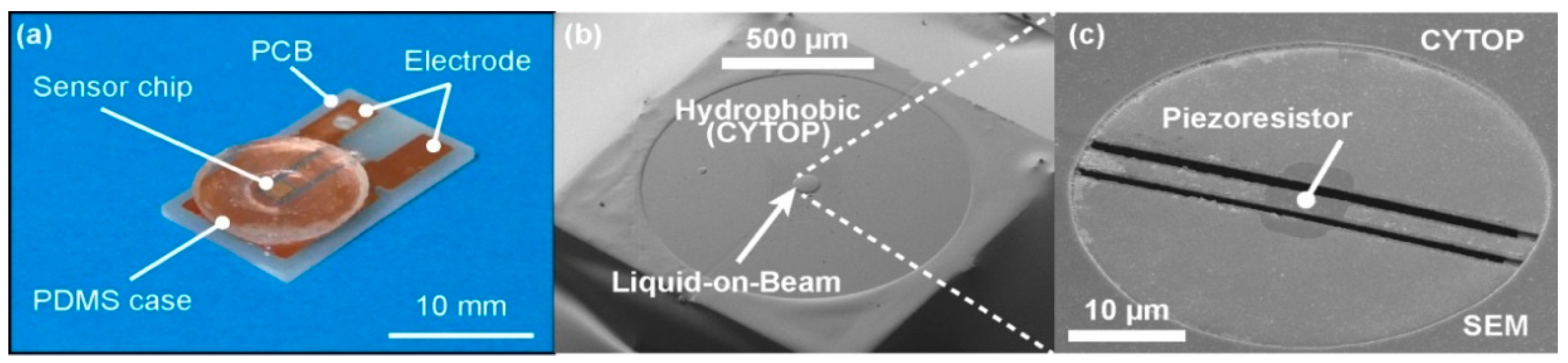
Figure 1 and Figure 2 show the basic structure of the SA sensor [14]. The SA sensor roughly comprises of four parts: a sensor chip, polydimethylsiloxane (PDMS), a printed circuit board (PCB) and an Au/Cr electrode. A very thin 300 nm beam is formed on the center of a Si sensor chip. The sensor chip was fabricated from Silicon on Insulator (SOI) wafer to facilitate forming thin beam. At the first step of the fabrication process, the n-type piezoresistive area was formed with either Ion implantation or thermal diffusion on the surface of the wafer. Then, the Au/Cr electrode was deposited and patterned with inductively coupled plasma reactive ion etching (ICP-RIE). The double-supported beam was also made during the ICP-RIE process. The Au layer was etched again to expose the piezoresistive area and form the electrode. The backside Si layer was etched as a cylindrical shape with ICP-RIE, and the SiO2 layer was etched with HF vapor to release the beam. On the surface of the chip, hydrophobic CYTOP (Asahi Glass Co., Ltd., Chiyoda-ku, Tokyo, Japan) was shaped as a band ring pattern. The liquid (silicone oil) was dropped on the beam. Taking advantage of the surface tension of the silicone oil and properly limiting the size of the gap between the beam and surrounding chip below 1 μm, leakage of the oil was completely prevented. Furthermore, due to the hydrophobicity of the CYTOP ring, an appropriate amount of liquid was automatically kept inside the ring. The parylene film was deposited on the chip surface to stabilize the liquid. The chip was bonded to the PCB with adhesive material, and both chip and PCB electrodes were wire-bonded. Finally, an appropriate amount of PDMS was mounted on the parylene film to form a fixed area to receive the lower frequency vibrations.
To keep the preferred sound impedance matching, the PCB side of the sensor was placed on a measuring object. When an acoustic emission signal is propagated into the sensor from the PCB side, the beam vibrates in accordance with the liquid surface. The advantage of this structure is that the vibration in accordance with the liquid surface is completely independent of the intrinsic eigenfrequency of the beam in the air. By measuring the shape of the beam with a laser scanning vibrometer, it was revealed that the vibration shape of the beam was dominated by the surface wave of the liquid, rather than its structural eigenfrequency. As a result, the sensor can receive quite a wide frequency range of vibrations, which cannot easily be achieved by resonant-type MEMS sensors.
3. Pencil Lead Break Tests
3.1. Pencil Lead Break Specification
Pencil lead break tests were done in accordance with the ASTM (American Society for Testing and Materials) specification [17,18]. The diameter and hardness of the lead are 0.5 mm and 2H, respectively. The length of the lead to be broken is set to be about 3 mm. Each break is performed at the same point, in the same direction. To maintain repeatability, it is preferable to adopt the Nielsen shoe during the PLB test. By pressing the tip of the lead onto the surface of an elastic material and breaking the lead, the pressure at the point on the lead is instantly released. Then, an elastic wave is generated from the breaking point. Figure 3 shows the schematic image of the PLB test.
3.2. Experimental Setup
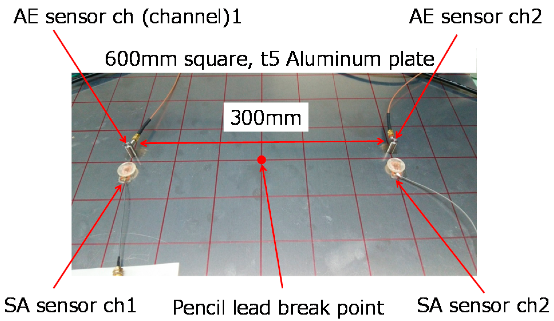
Figure 4 and Figure 5 show the experimental setup of this paper. 600 × 600 mm and t5.0 mm aluminum plate is adopted. There are three points on the plate for the PLB test, center of the plate, 75 mm left from the center and 75 mm right from the center. SA sensors are placed 150 mm apart from the center of the plate. To compare the AE waveform received by the SA sensor, an AE sensor is plated on the near side of each SA sensor. To reflect a typical resonant-type AE sensor suitable for metallic structure, AE144A (Vallen Systeme GmbH, Icking, Germany) was selected.
4. Pencil Lead Break Results
Figure 6 shows the waveform of a PLB test obtained by the AE sensor. In this test, the lead was broken at the center of the plate. These two graphs show that the initial in-plane s0 wave propagates within 20 μs after each sensor crosses the preset threshold and is triggered. Then, the out-of-plane a0 wave subsequently reaches the sensors. To examine the time series of frequency distribution, the obtained data was analyzed by wavelet transform. Figure 7 shows the result of wavelet transform. The red line and the deep green line show the theoretical arrival time of the s0 mode and a0 mode, respectively. In this experiment, the AE sensor properly detected the s0 mode which has an approximately 200 kHz to 400 kHz frequency bandwidth. The a0 mode was also received by AE sensor, and the figure shows that the a0 mode has a 100 kHz to 500 kHz frequency bandwidth.
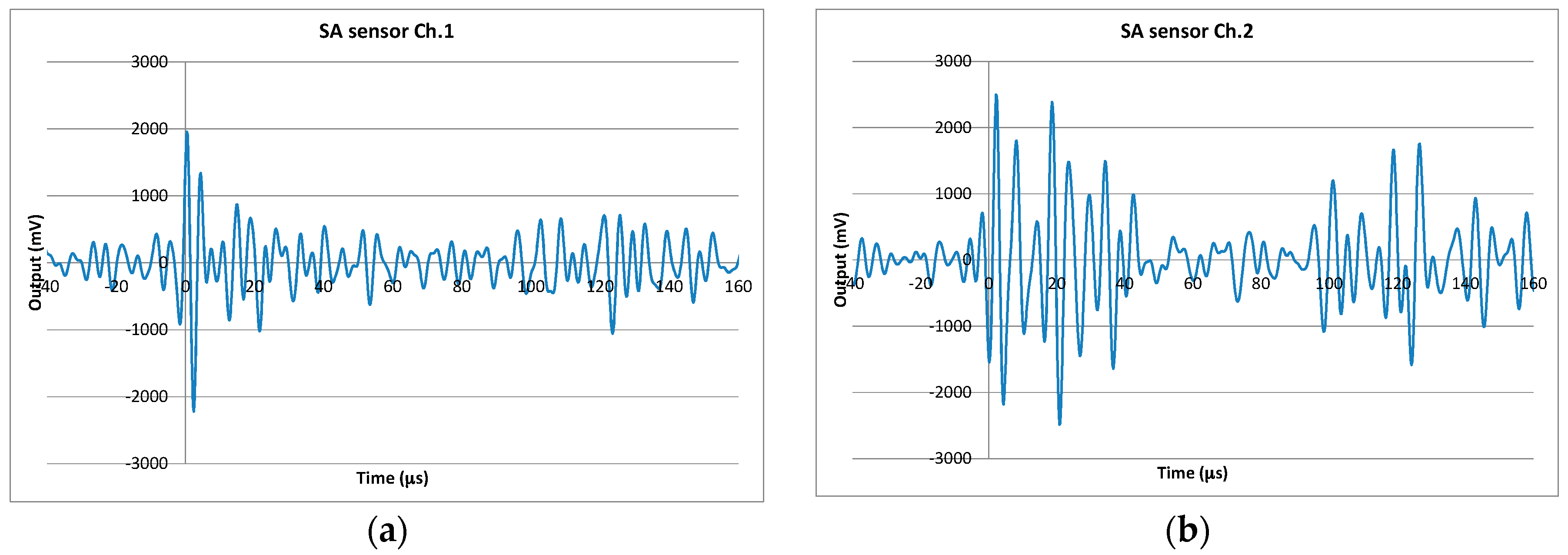
Figure 8 shows the waveform of the same PLB test obtained by the SA sensor. To examine the time series of frequency distribution, the result of wavelet transform of each output is shown in Figure 9. Red line, deep green line and yellow line show the theoretical arrival time of the s0 mode, a0 mode and a1 mode, respectively. From the result of wavelet transform, it is obvious that the a0 mode is properly detected by the SA sensors. On the other hand, the s0 mode is not obvious, compared to the a0 mode. From the viewpoint of the relationship between triggered time and wavelet transform, the preset threshold is crossed by the a0 mode. It can be said that, although the SA sensor obviously receives the PLB originated elastic wave, the threshold is crossed by the a0 mode. The main difference of these figures compared to the AE sensor results is that the SA sensor signal includes the higher frequency spectrum between 200 kHz and 350 kHz, especially in ch.2 of the SA sensor. In the AE sensor results, this component is not clearly shown, especially between 40 μs and 80 μs. In this period, as shown in the theoretical arrival time for each elastic wave plotted in color line, the a1 mode is superior to the other modes at around 350 kHz. This result shows that SA sensor ch.2 properly received the a0 and subsequent a1 modes due to its wide frequency characteristics. In the same period, the AE sensor has a strong 140 kHz frequency component and a very weak 300 kHz component, as shown in Figure 7. This is because the AE sensor vibrated in accordance with the natural frequency of internal PZT. However, this AE sensor is not designed to receive at around 350 kHz, so the sensor couldn’t clearly receive the a1 mode. The strong frequency component in the SA sensor at around 200 kHz was caused by the frequency characteristics of the SA sensor itself. Although the SA sensor shows wide frequency characteristics, the sensitivity of the sensor varies depending on the frequency. The frequency characteristics are affected by the structure of sensor, such as the amount of liquid, the thickness of the parylene film, etc.
5. Time Difference and Source Location
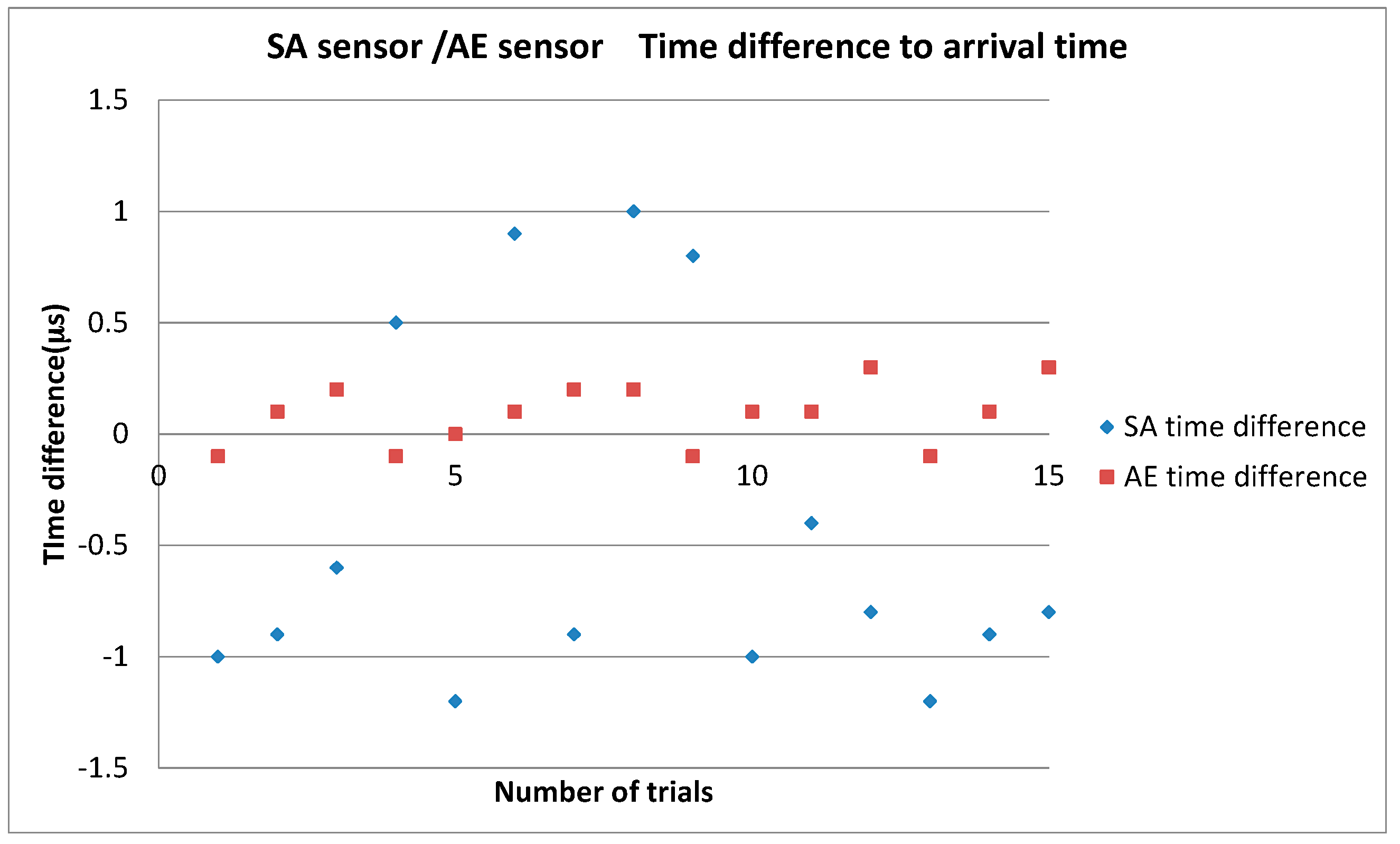
Figure 10 shows the time difference between each SA and AE sensor during the PLB test. The data is sampled with a sampling frequency of 10 MHz. The point of PLB is the center of the plate, thus the time difference of each SA and AE sensor ideally becomes zero. From this result, the deviation of time difference shown in the AE sensor result is smaller than the SA result. However, with regard to the velocity of the s0 and a0 modes of about 5000 m/s and 3300 m/s respectively, 1 μs time difference could simply reflect a 2.5 mm or 1.6 mm location error. This location error is only 0.8% and 0.5% length of the actual sensor distance. From these result, the SA sensor has enough potential to be used as the sensor for source location of a PLB test.
6. Discussion
The time difference of SA sensor shown in the Figure 10 is sufficiently small. But the s0 mode is almost not detected in Figure 9. One of the reasons is that the sensor chip is located at the bottom of the sensor. Because the s0 mode is propagated inside the aluminum plate with symmetric deformation, the vibration of the beam inside the sensor chip is not properly excited. On the other hand, the a0 mode causes the asymmetric deformation in the plate. Then, the vibration of the beam is efficiently excited. This implies that the direction of the beam inside the sensor is a crucial parameter to properly receive the aimed elastic wave [19].
7. Conclusions
Elastic waves generated by PLB tests were measured by both SA and AE sensors. Time series frequency characteristics were analyzed by wavelet transform. The SA sensor was triggered by the out-of-plane a0 mode, though the AE sensor was triggered by the in-plate s0 mode. The SA sensor has sufficient potential to be used as the sensor for source location of PLB tests.
Acknowledgments
This work was supported by the New Energy and Industrial Technology Development Organization (NEDO).
Author Contributions
M.-D.N., K.M. and I.S. designed and made the MEMS sensor and the preamplifier; T.O., T.U. and K.W. conceived and designed the experiments; T.O. performed the experiments; T.O. and T.U. analyzed the data; T.O. wrote the paper.
Conflicts of Interest
The authors declare no conflict of interest. The founding sponsors had no role in the design of the study; in the collection, analyses, or interpretation of data; in the writing of the manuscript; or in the decision to publish the results.
References
- Shiotani, T.; Osawa, S.; Momoki, S.; Ohtsu, H. Visualization of Damage in RC Bridge Deck for Bullet Trains with AE Tomography, Advances in Acoustic Emission Technology. In Springer Proceedings in Physics; Springer: New York, NY, USA, 2015; Volume 158. [Google Scholar]
- Nishida, T.; Shiotani, T.; Asaue, H.; Maejima, T.; Kobayashi, Y. Damage Evaluation of RC Bridge Deck under Wheel Loading Test by Means of AE. Tomography. In Proceedings of the 8th International Conference on Acoustic Emission, Kyoto, Japan, 5–9 December 2016; pp. 111–116. [Google Scholar]
- Pham, Q.K.; Nguyen, M.D.; Nguyen, B.K.; Phan, H.P.; Matsumoto, K.; Isao, S. Multi-axis force sensor with dynamic range up to ultrasonic. In Proceedings of the IEEE MEMS, San Francisco, CA, USA, 26–30 January 2014; pp. 474–482. [Google Scholar]
- Kaneko, T.; Nguyen, M.D.; Pham, Q.K.; Takei, Y.; Takahata, T.; Matsumoto, K.; Shimoyama, I. Pulse wave measurement in human using piezoresistive cantilever on liquid. In Proceedings of the IEEE MEMS, Estoril, Portugal, 18–22 January 2015; pp. 2083–2092. [Google Scholar]
- Pham, Q.K.; Nguyen, M.D.; Matsumoto, K.; Shimoyama, I. Acoustic Emission Sensor using Liquid-on-Beam Structure. In Proceedings of the IEEE Transducers, Anchorage, Alaska, 21–25 June 2015; pp. 1137–1139. [Google Scholar]
- Ozevin, D.; Greve, D.W.; Oppenheim, I.J.; Pessiki, S.P. Resonant capacitive MEMS acoustic emission transducers. Smart Mater. Struct. 2006, 15, 1863. [Google Scholar] [CrossRef]
- Saboonchi, H.; Ozevin, D. In-Plane MEMS Acoustic Emission Sensors Development and Experimental Characterization. MEMS Nanotechnol. 2014, 5, 81–87. [Google Scholar]
- Greve, D.W.; Oppenheim, I.J.; Wu, W.; Wright, A.P. Development of a MEMS acoustic emission sensor system. Proc. SPIE 2007, 6529, 652912. [Google Scholar]
- Oppenheim, I.J.; Jain, A.; Greve, D.W. Electrical Characterization of Coupled and Uncoupled MEMS Ultrasonic Transducers. IEEE Trans. Ultrason. Ferroelectr. Freq. Control 2003, 50, 297–304. [Google Scholar] [CrossRef] [PubMed]
- Oppenheim, I.J.; Jain, A.; Greve, D.W. MEMS Ultrasonic Transducers for the Testing of Solids. IEEE Trans. Ultrason. Ferroelectr. Freq. Control 2003, 50, 305–311. [Google Scholar] [CrossRef] [PubMed]
- Pickwell, A.J.; Dorey, R.A.; Mba, D. Development of a Thick Film PZT Foil Sensor for Use in Structural health Monitoring Applications. IEEE Trans. Ultrason. Ferroelectr. Freq. Control 2013, 60, 373–379. [Google Scholar] [CrossRef] [PubMed]
- Feng, G.H.; Tsai, M.Y. Acoustic emission sensor with structure-enhanced sensing mechanism based on micro-embossed piezoelectric polymer. Sens. Actuators A 2010, 162, 100–106. [Google Scholar] [CrossRef]
- Khir, M.H.M.; Qu, P.; Qu, H. A Low-Cost CMOS-MEMS Piezoresistive Accelerometer with Large Proof Mass. Sensors 2011, 11, 7892–7907. [Google Scholar] [CrossRef] [PubMed]
- Takahashi, H.; Nguyen, M.D.; Matsumoto, K.; Shimoyama, I. Differential pressure sensor using a piezoresistive cantilever. J. Micromech. Microeng. 2012, 22, 055015. [Google Scholar] [CrossRef]
- Omori, T.; Usui, T.; Watabe, K.; Nguyen, M.D.; Matsumoto, K.; Shimoyama, I. Elastic Wave Measurement using a MEMS AE Sensor. In Proceedings of the 8th International Conference on Acoustic Emission, Kyoto, Japan, 5–9 December 2016; pp. 339–344. [Google Scholar]
- Nguyen, M.D.; Pham, Q.K.; Matsumoto, K.; Shimoyama, I. MEMS Based Acoustic Emission sensor. In Proceedings of the AEWG-58, Philadelphia, PA, USA, 22–25 May 2016. [Google Scholar]
- Standard Guide for Determining the Reproducibility of Acoustic Emission Sensor Response; ASTM E976-10; American Society for Testing and Materials: Philadelphia, PA, USA, 2010.
- Hamstad, M.A. Acoustic Emission Signals Generated by monopole (Pencil-Lead Break) versus Dipole Sources: Finite Element modeling and Experiments. J. Acoust. Emiss. 2007, 25, 92–106. [Google Scholar]
- Matsuda, N.; Nguyen, M.D.; Takahata, T.; Shimoyama, I. A multi-axis piezoresistive MEMS sensor for acoustic emission. In Proceedings of the IEEE MEMS, Las Vegas, NV, USA, 22–26 January 2017; pp. 1181–1183. [Google Scholar]
Figure 1.
Schematic (a) bird’s eye and (b) cross-sectional view of super acoustic (SA) sensor. Abbreviations and products: PDMS, polydimethylsiloxane; HIVAC-F4, obtained from Shin-Etsu Silicones (Chiyoda-ku, Tokyo, Japan); CYTOP, obtained from Asahi Glass Co., Ltd. (Chiyoda-ku, Tokyo, Japan).
Figure 1.
Schematic (a) bird’s eye and (b) cross-sectional view of super acoustic (SA) sensor. Abbreviations and products: PDMS, polydimethylsiloxane; HIVAC-F4, obtained from Shin-Etsu Silicones (Chiyoda-ku, Tokyo, Japan); CYTOP, obtained from Asahi Glass Co., Ltd. (Chiyoda-ku, Tokyo, Japan).
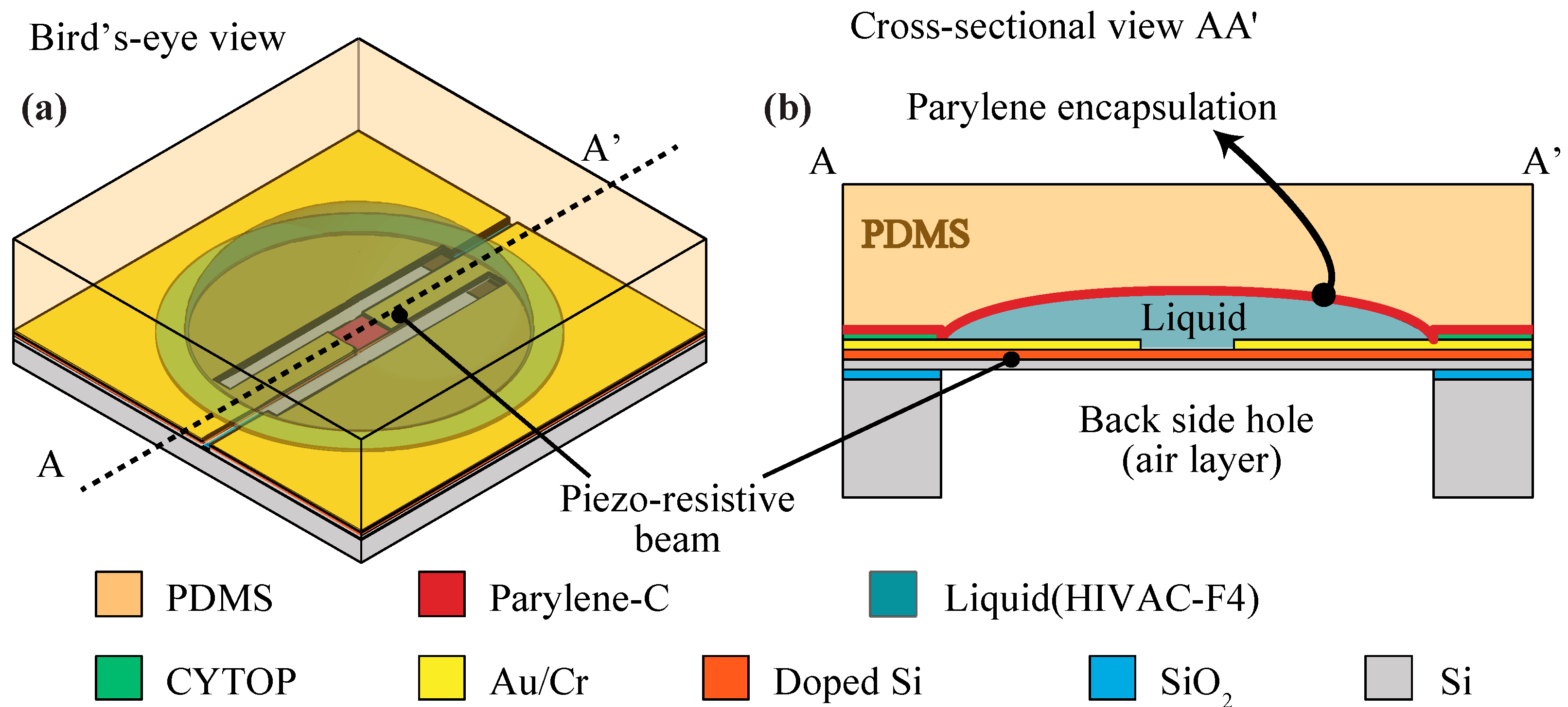
Figure 2.
(a) SA sensor appearance, (b) SEM (scanning electron microscope) image of sensor chip and (c) SEM image of n-type doped piezoresistive area.
Figure 2.
(a) SA sensor appearance, (b) SEM (scanning electron microscope) image of sensor chip and (c) SEM image of n-type doped piezoresistive area.

Figure 3.
Pencil lead break test.
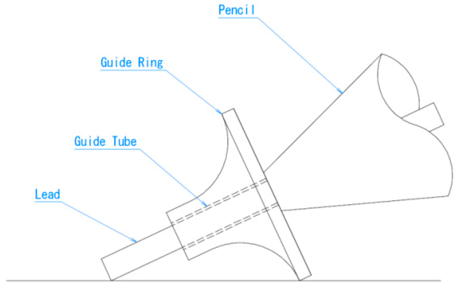
Figure 4.
Block diagram of PLB test. Abbreviations and products: AMSY-6, AEP3N, and AE144A, obtained from Vallen Systeme GmbH (Icking, Germany); 9913, obtained from NF Corporation (Yokohama, Kanagawa, Japan); U-Tokyo, The University of Tokyo; SA, Super Acoustic.
Figure 4.
Block diagram of PLB test. Abbreviations and products: AMSY-6, AEP3N, and AE144A, obtained from Vallen Systeme GmbH (Icking, Germany); 9913, obtained from NF Corporation (Yokohama, Kanagawa, Japan); U-Tokyo, The University of Tokyo; SA, Super Acoustic.
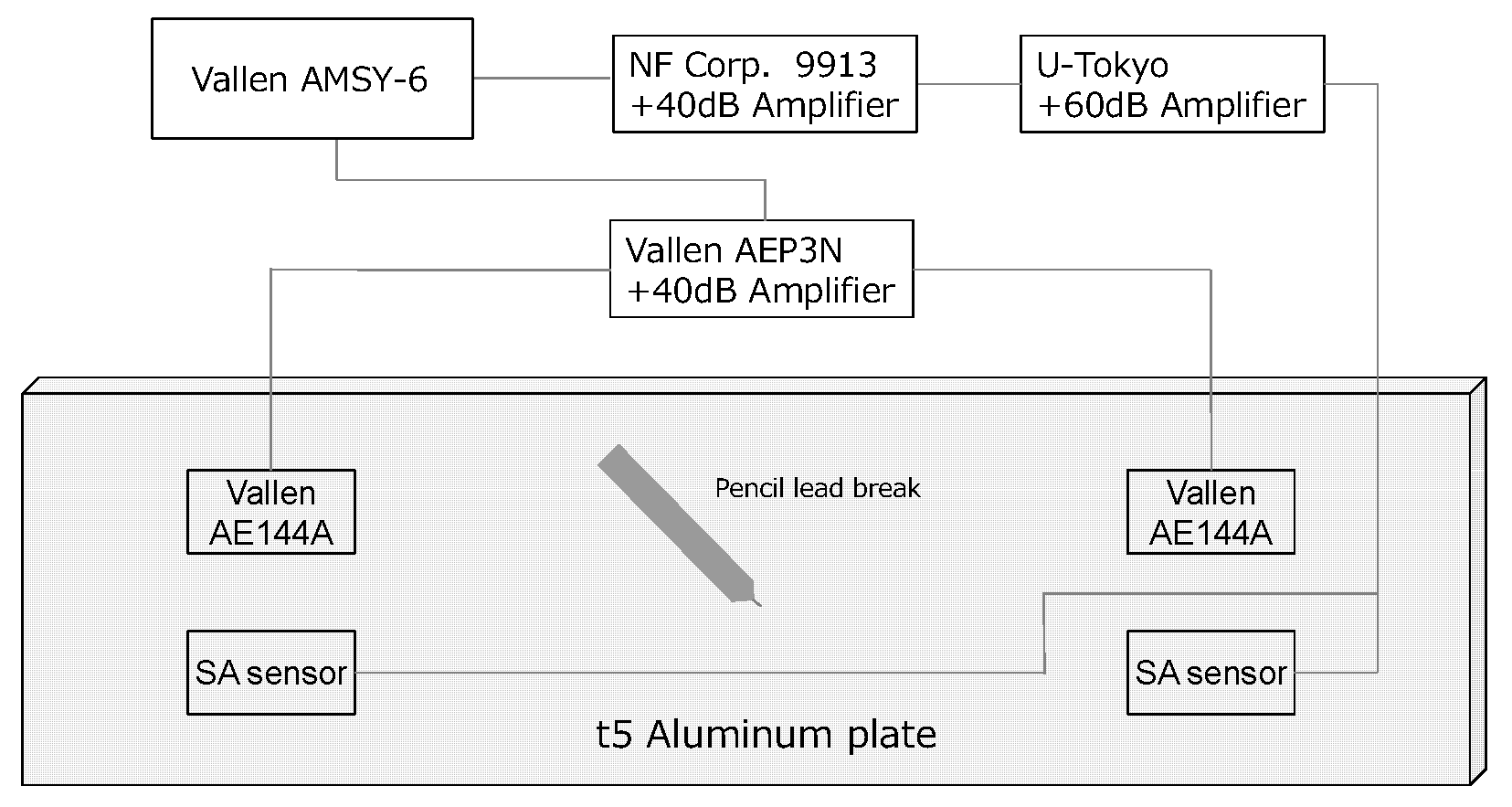
Figure 5.
Experimental setup of SA and AE (acoustic emission) sensors.

Figure 6.
Waveform of AE sensor (a) ch.1 and (b) ch.2.
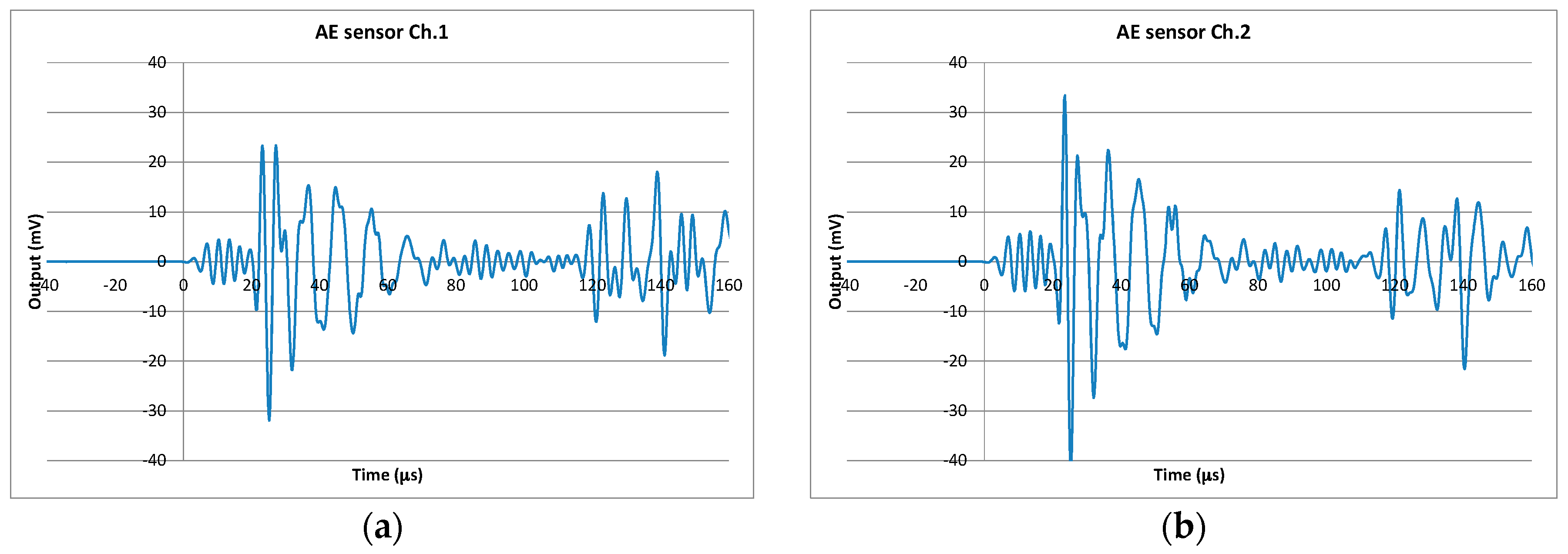
Figure 7.
Wavelet transform of AE sensor (a) ch.1 and (b) ch.2.

Figure 8.
Waveform of SA sensor (a) ch.1 and (b) ch.2.

Figure 9.
Wavelet transform of SA sensor (a) ch.1 and (b) ch.2.
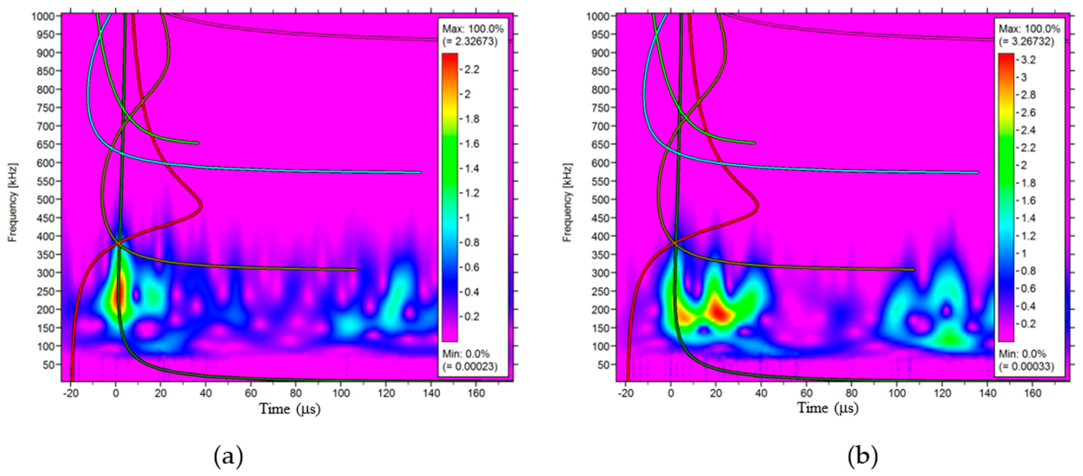
Figure 10.
Time difference between each SA/AE sensor pair.

© 2017 by the authors. Licensee MDPI, Basel, Switzerland. This article is an open access article distributed under the terms and conditions of the Creative Commons Attribution (CC BY) license (http://creativecommons.org/licenses/by/4.0/).
Share and Cite
MDPI and ACS Style
Omori, T.; Usui, T.; Watabe, K.; Nguyen, M.-D.; Matsumoto, K.; Shimoyama, I. Elastic Wave Measurement Using a MEMS AE Sensor. Appl. Sci. 2017, 7, 737. https://doi.org/10.3390/app7070737
AMA Style
Omori T, Usui T, Watabe K, Nguyen M-D, Matsumoto K, Shimoyama I. Elastic Wave Measurement Using a MEMS AE Sensor. Applied Sciences. 2017; 7(7):737. https://doi.org/10.3390/app7070737
Chicago/Turabian StyleOmori, Takahiro, Takashi Usui, Kazuo Watabe, Minh-Dung Nguyen, Kiyoshi Matsumoto, and Isao Shimoyama. 2017. "Elastic Wave Measurement Using a MEMS AE Sensor" Applied Sciences 7, no. 7: 737. https://doi.org/10.3390/app7070737
Note that from the first issue of 2016, this journal uses article numbers instead of page numbers. See further details here.