A Compact and Multi-Stack Electromagnetic Bandgap Structure for Gigahertz Noise Suppression in Multilayer Printed Circuit Boards


1
Department of Electrical, Electronic, and Control Engineering, Institute for Information Technology Convergence, Hankyong National University, Anseong 17579, Korea
2
The Cho Chun Shik Graduate School for Green Transportation, Korea Advanced Institute of Science and Technology (KAIST), Daejeon 34141, South Korea
*
Author to whom correspondence should be addressed.
Appl. Sci. 2017, 7(8), 804; https://doi.org/10.3390/app7080804
Submission received: 28 June 2017
/
Revised: 25 July 2017
/
Accepted: 31 July 2017
/
Published: 7 August 2017
(This article belongs to the Special Issue Printed Electronics 2017)
Abstract
:In modern printed electronics, the performances of a circuit and a device are severely deteriorated by the electromagnetic noise in the gigahertz (GHz) frequency range, such as the simultaneous switching noise and ground bounce noise. A compact and multi-stack electromagnetic bandgap (CMS-EBG) structure is proposed to suppress the electromagnetic noise over the GHz frequency range with a short distance between a noise source and a victim on multilayer printed circuit boards (MPCBs). The original configuration of the stepped impedance resonators is presented to efficiently form multiple stacks of EBG cells. The noise suppression characteristics of the CMS-EBG structure are rigorously examined using Floquet-Bloch analysis. In the analysis, dispersion diagrams are extracted from an equivalent circuit model and a full-wave simulation model. It is experimentally verified that the CMS-EBG structure suppresses the resonant modes over the wideband frequency range with a short source-to-victim distance; thus, this structure substantially mitigates GHz electromagnetic noise in compact MPCBs.
1. Introduction
The multilayer printed circuit board (MPCB) technology is widely used in recent printed electronics. It provides a reliable and cost-effective manufacturing process and simply realizes high-speed interconnects, power buses, and passive planar components. MPCBs are used for various electronic applications including radio-frequency (RF) circuits, microwave circuits, and high-speed digital circuits. With the rapidly growing demand for electronics with massive computation capability and a small form factor, the MPCB technology has been significantly developed for mixed-signal applications, where high-speed digital devices and wireless communication devices are integrated in the same MPCBs.
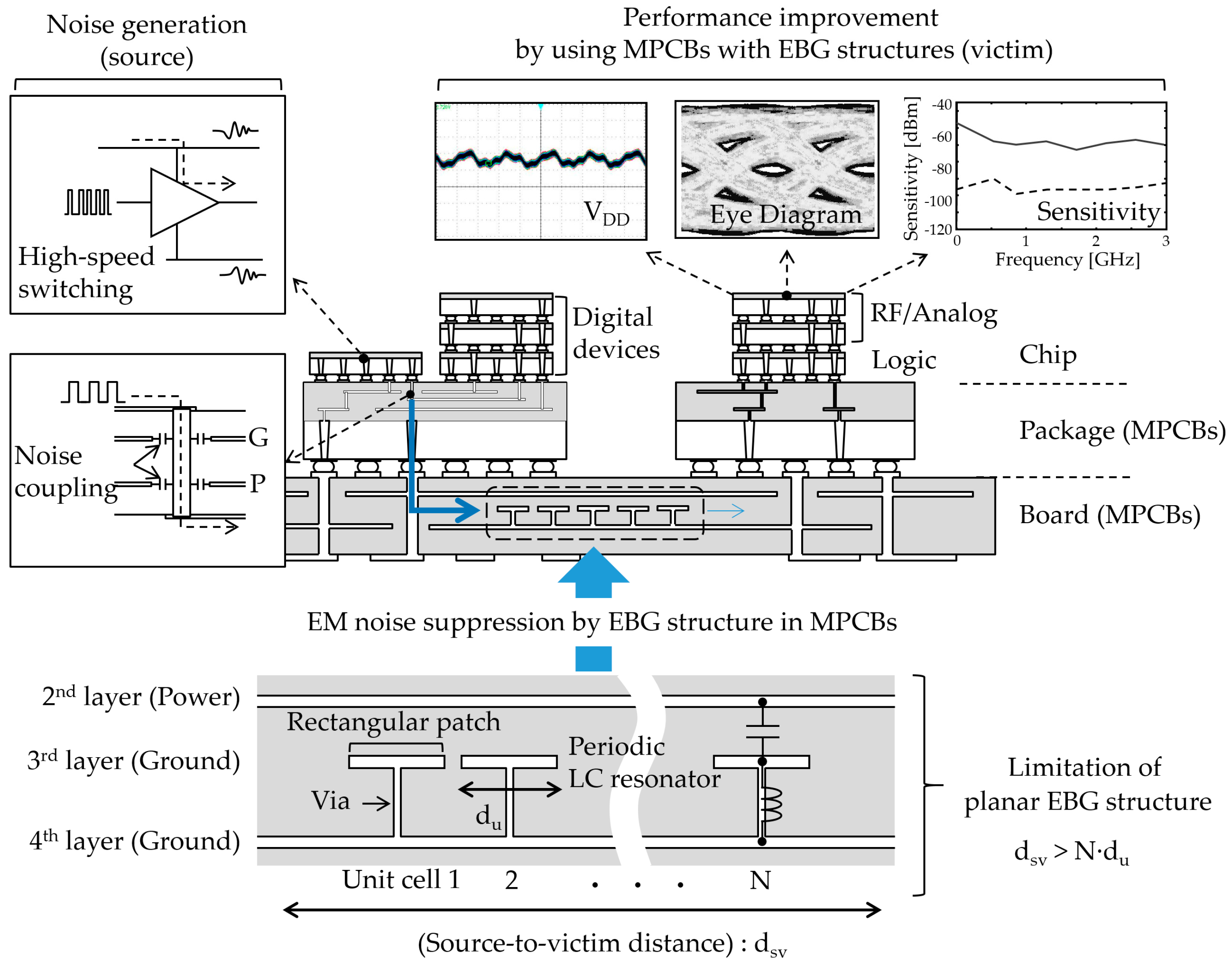
Mixed-signal MPCBs support the complex configuration of RF, analog, and digital devices, as shown in Figure 1. Various devices such as RF, analog, memory, and digital chips are mounted on the MPCBs. Digital devices are known to generate wideband electromagnetic noise in the gigahertz (GHz) frequency range, which severely degrades the performance of the other circuits including themselves [1,2,3,4,5]. In addition, the noise source and victim devices are placed closely for the compact design. The wideband GHz-noise coupling in a compact area reduces the voltage margin, deteriorates the eye-diagram characteristics, and decreases the receiver sensitivity. In particular, the GHz-noise coupling through direct current (DC) power buses in MPCBs is a significant problem [6,7,8,9]. In mixed-signal MPCBs, DC power buses are essential for properly delivering power to the circuits. Power buses connect the chips with power sources such as the regulator and DC/DC converter. The power buses are patterned on any metal layer in the MPCBs. The power buses are mostly designed by using solid metal planes to reduce the design complexity. Considering the electromagnetic wave theory, the electromagnetic characteristics of the previous power buses are equivalent to a parallel plate waveguide (PPW). In a PPW-based power bus of mixed-signal MPCBs, numerous resonant modes in the wideband frequency range are excited, which induces the GHz electromagnetic noise couplings between a noise source and a victim [6,7,8,9]. Moreover, the short horizontal distance from a noise source to a victim device for a compact system results in a severe electromagnetic interference. Consequently, wideband noise suppression with a short distance between the noise source and the victim is required for the high performance of MPCBs.
Numerous studies are presented to suppress the resonant modes of a PPW in the GHz frequency range. In particular, electromagnetic bandgap (EBG) structures show vastly superior characteristics to suppress the resonant modes in a wideband frequency range [10,11,12,13,14,15,16,17,18,19,20]. The EBG structure is the engineered material used to obtain a broad stopband, where the propagation of a GHz noise wave is prevented. In the EBG structure, unit cells (UCs) are periodically arranged in the same horizontal plane. The UCs may include an equivalent LC resonator or a stepped impedance resonator to suppress the GHz electromagnetic noise. The previous EBG structures have the advantage of a wideband stopband in the GHz frequency range. However, the previous EBG structures are designed based on a planar structure, so they require a sufficiently large number of UCs that are placed horizontally between a noise source and a noise victim. In other words, a large horizontal distance from the source to the victim is required. As shown in Figure 1, the source-to-victim distance is equivalent to the product of the number and the size of EBG UCs, which are substantially large. To reduce the horizontal area of the EBG structure, the multi-layer EBG structures with LC resonators are presented [21,22]. However, they did not focus on reducing the source-to-victim distance. To maintain or enhance the characteristics of the previous EBG structures, it is inevitable to place the large number of EBG UCs, which increase the horizontal distance between the source and the victim. However, in modern MPCBs, various mixed-signal devices must be densely placed in a small area. Consequently, the use of the previous EBG structures for compact applications is severely limited. Thus, it is necessary that an EBG structure is designed to occupy a compact area and substantially reduce the source-to-victim distance with the wideband GHz noise suppression in MPCBs.
In this article, a compact and multi-stack electromagnetic bandgap (CMS-EBG) structure with a short source-to-victim distance is proposed using vertically stacked UCs and the original stepped impedance configuration. The proposed method significantly reduces the horizontal area of the EBG structure and the source-to-victim distance with a wideband suppression of the GHz-electromagnetic noise. The simulation and measurements verify the characteristics of the proposed CMS-EBG structure.
2. Design of Compact and Multi-Stack Electromagnetic Bandgap (CMS-EBG) Structure
2.1. Geometrical Design
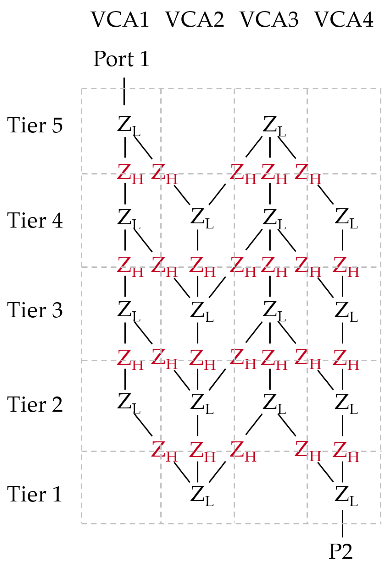
The CMS-EBG structure is designed to exhibit a wideband suppression of GHz noise with a compact area and a short source-to-victim distance. To achieve this objective, a multi-stack technique is applied to the CMS-EBG structure. The multi-stack technique is the original configuration of a stepped impedance resonator, which consists of a low-characteristic-impedance (low-Zo) part and a high-Zo part. As illustrated in Figure 2a, the low-Zo part consists of a rectangular-shape low-Zo patch in a power layer (P) and two rectangular planes (G) in the ground layers (G), which are located above and below the low-Zo patch. The dielectric material is located between the power and ground layers. The high-Zo part is formed by two narrow high-Zo patches and a via structure. The high-Zo patches are placed in different layers and connected through the via structure. The high-Zo part is denoted as a vertical-cell-array (VCA) branch. The ground via structures should be placed adjacent to the VCA branch, but the ground vias are not shown in Figure 2a for simplicity. The ground via is described in detail in Figure 4. In addition to the VCA branch, the term ‘VCA’ implies a vertical stack of low-Zo patches. The CMS-EBG structure contains four VCAs as shown in Figure 2a. Each VCA includes a stack of four low-Zo patches. To explain the CMS-EBG structure, a unit cell is defined as the low-Zo parts with half of the VCA branches as shown in Figure 2a. The notation UC(i,j) is adopted to express the unit cell in the i-th VCA and j-th tier.
The VCA branch was originally developed to connect low-Zo patches in different tiers or different UCs. Two types of connection between low-Zo patches in different tiers are considered in the CMS-EBG structure. First, low-Zo patches in different tiers but the same VCA are considered, which is called an intra-VCA branch. In Figure 2a, the intra-VCA branch is highlighted with a blue dashed line, which connects the low-Zo patches in UC(4,2) to UC(4,3). The other type is an inter-VCA branch, which connects low-Zo patches in different tiers and different VCAs. In Figure 2a, for instance, the inter-VCA branch is highlighted to connect a low-Zo patch in UC(3,5) to a low-Zo patch in UC(4,4). To more clearly explain the intra-/inter-VCA branches, only the low-Zo patches and VCA branches are shown in the other view point in Figure 2b, where the red and blue arrows point at the inter-VCA branches and intra-VCA branches, respectively. All low-Zo patches have one or two intra-VCA branches. For the inter-VCA branch, the low-Zo patches in VCA 1 and VCA 4 contain one inter-VCA branch, whereas each low-Zo patch in VCA 2 and VCA 3 contains two inter-VCA branches. For example, UC(1,5) has an intra-VCA branch to connect with UC(1,5) and an inter-VCA branch to connect with UC(2,4). For UC(3,5), two inter-VCA branches are used to connect with UC(2,4) and UC(4,4), whereas one intra-VCA branch connects it to UC(3,4). In summary, the intra-VCA branch connects the UCs in different tiers but the same VCA, whereas the inter-VCA branch connects the UCs in different tiers and different VCAs.
Due to the original configuration of the UCs and VCA branches, the CMS-EBG structure is able to place numerous EBG cells in a compact horizontal area of MPCBs. The CMS-EBG structure in Figure 2 contains sixteen EBG cells, which is equivalent to a 4 × 4 array of the previous planar EBG structure. Remarkably, the CMS-EBG structure occupies only a 2 × 2 array horizontally, which is a quarter of the size of the previous EBG array. Furthermore, the number of EBG cells is not limited to the number herein. It can be extended for a larger number of EBG cells with more layers. In many applications of MPCBs, such as cloud server systems and massive computational devices, the planar area occupied by an EBG structure is more significant than the layer number in an EBG structure. Hence, a multi-stack technique in the CMS-EBG structure is valuable for MPCBs. Moreover, the multi-stack technique has another advantage. All VCA branches are consistently formed by the same narrow patches and via structures using the multi-stack technique. The consistent use of the VCA branch ensures that the electromagnetic characteristics of the CMS-EBG structure can be simply modeled and analyzed using the theory of a periodic structure.
2.2. Characteristic–Impedance Analysis
The principle of noise suppression of the CMS-EBG structure is based on the stepped impedance resonator. To explain the noise suppression characteristics, a lattice diagram for the characteristic impedance (Zo-lattice diagram) is extracted from the CMS-EBG structure as shown in Figure 3. The characteristic impedances and the associated physical geometries of the unit cells are shown in the Zo-lattice diagram. The aforementioned low-Zo part is represented as ZL, and the high-Zo part of the VCA branch is represented as ZH. The Zo-lattice diagram describes the relationship between the unit cells considering the electromagnetic wave theory. The Zo-lattice diagram shows that the stepped impedance characteristics are formed in the CMS-EBG structure, and the low- and high-Zo parts are two-dimensionally and quasi-periodically arranged. The multi-stack technique achieves the 3-D physical geometry of the EBG structure which contains a 2-D lattice structure of the characteristic impedances.
In the Zo-lattice diagram, adjacent low-Zo parts (ZL) in the same tier are not connected with one another. Each low-Zo part connects to the low-Zo parts in different tiers through the high-Zo parts. All connections between the low-Zo parts are implemented by the same VCA branches represented as ZH. Thereby, the stepped impedance characteristics of the CMS-EBG structure are symmetric and periodical, whereas the physical structure is three-dimensionally complex for the compact form factor. The 2-D periodic arrangement without a defect ensures a broadband stopband and a simple estimation of the stopband using a dispersion analysis for the periodic structure. This distinguished characteristic of the CMS-EBG structure is accomplished by a multi-stack technique based on the original configuration with VCA branches.
To obtain the wideband GHz noise suppression with an extremely short source-to-victim distance using the CMS-EBG structure, the port configuration needs to be further explained. In the CMS-EBG structure, a noise source and a victim can be connected to the unit cells in different tiers. Suppose that a noise source device and a victim device are mounted on the top or bottom layer of the CMS-EBG structure. Then, the noise source and victim can be vertically connected to UC(5,1) and UC(1,4), respectively, through the via structures. The lateral distance between the noise source and a victim is extremely short because UC(5,1) and UC(1,4) are closely placed in the horizontal view. However, the noise source and a victim are sufficiently separated in the view of the Zo-lattice diagram, as shown in Figure 3. Figure 2 and Figure 3 depict the locations of the noise source and victim, which are represented as Port 1 and Port 2. This configuration is fairly reasonable, and the usage of the CMS-EBG structure is not severely limited.
3. Floquet-Bloch Analysis
Floquet-Bloch analysis based on a unit cell is adopted to examine and estimate the stopband characteristics of the CMS-EBG structure. For a simple analysis, a new unit cell is defined, as shown in Figure 4a. The new definition of the unit cell is based on an irreducible Brillouin zone (IBZ) for the one-dimensional Floquet-Bloch analysis. The IBZ unit cell consists of half of the low-Zo patch, the corresponding ground planes, the VCA branch, and ground vias. The ground vias are not shown in Figure 2 for simplicity. However, the ground vias must connect all ground planes in the CMS-EBG structure as shown in Figure 4a.
The equivalent circuit for one-dimensional propagation through the IBZ unit cell is extracted in Figure 4b. Half of the low-Zo patch is equivalently modeled as a transmission line circuit with a characteristic impedance of ZoL, a propagation constant of β, and the length of WP/2 while the equivalent circuit model of the VCA branch is a series of inductors. The inductances Lb and Lv are induced from the narrow patch in the high-Zo patch and via structure, respectively. The inductance of the ground vias is ignored to simplify the calculation. To derive the dispersion characteristics under the assumption of the Bloch wave, the ABCD parameters of the equivalent circuits are considered. The relationship between ABCD parameters are given by
where,
The effective phase constant for the dispersion characteristics is obtained by calculating the Aeq component of the equivalent transmission line
where the effective inductance Leff of the VCA branch is 2Lb + LV. ZoL can be found using the equation in [14,19] and a computer-aided simulation. Lb and Lv are given by [23,24]
Using the effective phase constant βeff, the electromagnetic bandgap characteristics of the CMS-EBG structure are explored. To present the effects of the design parameters on the bandgap characteristics, example values of the design parameters (wp, wb, db, Sb, Sv, rv, t, h) are selected. wp is the length of the low-Zo patch. wb, db, and Sb are the width, length, and location of the high-Zo patch, respectively. rv is the radius of the via in the VCA branch and the ground vias. t is the thickness of the metal. h is the distance between metal layers. The nominal value of the design parameters wp, wb, db, Sb, Sv, rv, t and h are 11, 1, 1, 5, 1, 0.2, 0.017, and 0.1 mm, respectively, which are practical and widely used in MPCBs. From the geometrical values, Leff and ZoL can be calculated as 0.25 nH and 0.8 Ω, respectively. The dispersion diagrams are obtained in Figure 5 using equation (3) and the finite-element method (FEM) simulation [25].
It is shown that passbands and stopbands alternately appeared in the dispersion diagram of the CMS-EBG structure. The first stopband is formed in the frequency range from low- and high-cutoff frequencies, which are denoted as fL and fH. In the dispersion diagram of the example structure, the first stopband spans over the GHz frequency range. The extracted fL and fH values from Equation (3) are 1.98 GHz and 6.42 GHz, respectively. Those from the FEM simulation are 2.2 GHz and 6.1 GHz. The dispersion equation and the FEM simulation show good agreement. The bandwidth of the stopband is 4.2 GHz, which is sufficiently broad to suppress the electromagnetic noise in MPCBs. Hence, the CMS-EBG structure is expected to suppress the resonant modes in the frequency range and effectively mitigate the wideband GHz noise in MPCBs.
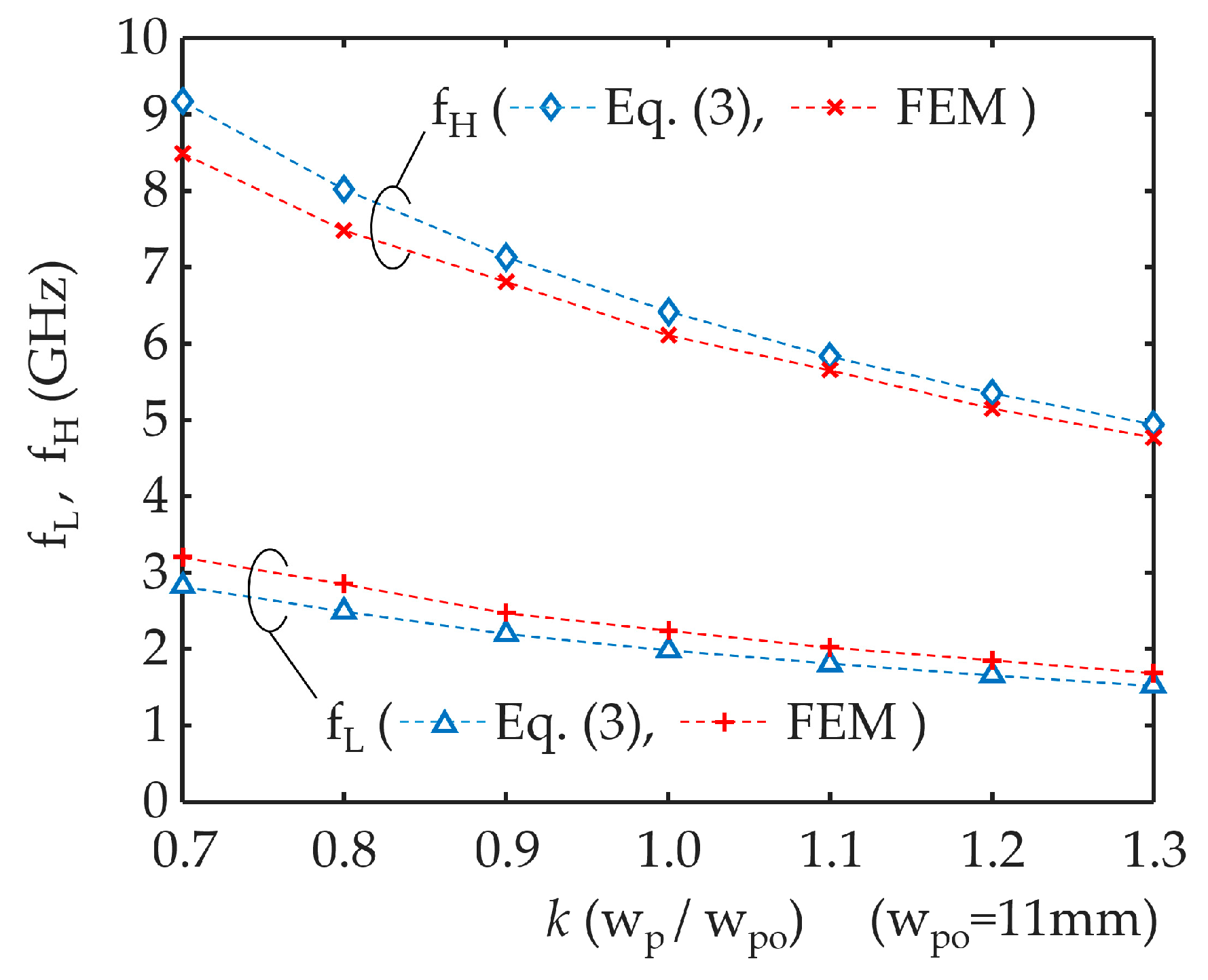
Furthermore, a sensitivity analysis is performed with the equation of the effective phase constant and FEM simulation to examine the effects of the main design parameter wp. In the analysis, the nominal values of wp, wb, db, Sb, Sv, rv, t and h are identical to those in Figure 5. fL and fH are calculated by sweeping the normalized coefficient k, which is defined as the ratio of a wp value to the nominal wp value (i.e., k = wp/wpo). k varies from 0.7 to 1.3 and the corresponding wp value varies from 7.7 mm to 14.3 mm with a nominal value of 11 mm. The extracted results of fL and fH are shown in Figure 6. For k = 0.7, fL and fH in Equation (3) are 2.82 GHz and 9.17 GHz, respectively; for k = 1.3, fL is 1.52 GHz, and fH is 4.94 GHz. The results derived from the FEM simulation show a good correlation with the results calculated using Equation (3). Hence, it is concluded that fL and fH are reduced as the wp increases.
The location and bandwidth characteristics of the stopband are additionally analyzed. The location of a stopband is characterized by the center frequency (fC), which is defined as (fL + fH)/2. The bandwidth characteristics are characterized by the fractional bandwidth (FBW), which is defined as (fH − fL)/fC. As seen in Figure 7a, the center frequency fC is shifted into the low-frequency range as wp increases. Conversely, the FBW does not significantly change as wp varies, as shown in Figure 7b. The FBW results obtained from the dispersion Equation (3) and FEM simulation are approximately 1.0 for various wp values. In other words, the CMS-EBG structure maintains approximately 100% fractional bandwidth characteristics for the various wp values. These characteristics enable a simple design of the CMS-EBG structure. The aforementioned dispersion characteristics of the CMS-EBG structure are summarized in Table 1. The ZoL values in Table 1 are obtained from the FEM simulation. The comparison results can be further summarized using the IEEE Standard for validation of the computational electromagnetics computer modeling and simulation with the feature selective validation (FSV) technique [26,27,28].
4. Results and Discussion
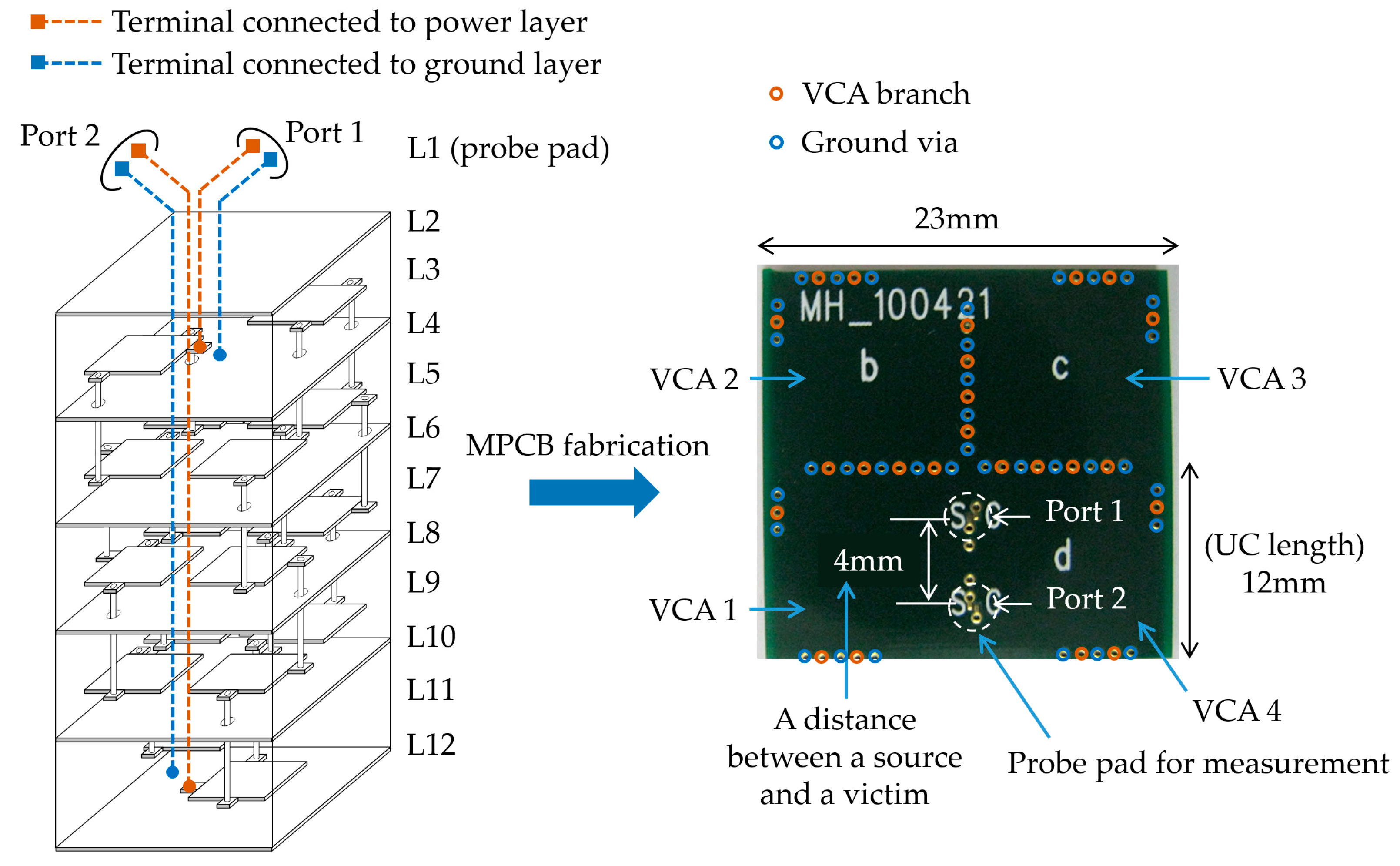
To verify the CMS-EBG structure, a test vehicle is fabricated using a commercial MPCB manufacturing process. The MPCB process provides twelve metal layers from L1 to L12. L1 is dedicated to probe pads for the measurements. The other layers are used for the CMS-EBG structure as shown in Figure 8. Copper and FR-4 are used for the conductor and dielectric material, respectively. The relative permittivity of the FR-4 is 4.4, and the loss tangent is 0.03. The copper thickness is approximately 17 μm. The distance between the layers (i.e., dielectric thickness) is 0.1 mm. The low-Zo patch, high-Zo patch, and ground plane are implemented by etching copper. A plated through hole (PTH) via is used in the MPCB process. The VCA branches and ground vias are made using the PTH vias. The MPCB process here is reliable, cost-effective, and easy to manufacture. Port 1 contains the signal terminal, which is connected to the high-Zo patch of UC(1,5) in L3 and the ground terminal, which is connected to the corresponding ground layers in L2 and L4. Port 2 consists of the signal terminal, which is connected to the high-Zo patch of UC(4,1) in L11. In addition, the ground terminal of Port 2 is connected to the corresponding ground layers in L10 and L12. The port configuration is equivalent to the ports in the Zo-lattice diagram in Figure 2a and Figure 3.
The top view of the CMS-EBG structure fabricated by the MPCB process is shown in Figure 8. The geometrical parameters are described in Figure 4 of Section 3. The values of the design parameters wp, wb, db, Sb, Sv, rv, t and h are 11, 1, 1, 5, 1, 0.2, 0.017, and 0.1 mm, respectively, which are equivalent to the values in the Floquet-Bloch analysis. The unit cell length is 12 mm. The distance between port 1 and port 2 is only 4 mm, which is less than the unit cell length. In addition, sixteen EBG cells are successfully located within a compact area of 23 mm × 23 mm, which is only one-quarter of the area that the previous 4 × 4 EBG structure requires.
The measurement setup is depicted in Figure 9. The scattering parameters (S-parameters) are measured using the vector network analyzer Agilent N5230A. The microprobe technology is used to minimize the parasitic effect induced by additional structures such as the measurement pad. The GS- and SG-type probes with 400 μm pitch are used. To analyze the noise suppression characteristics, a S21 parameter is observed.
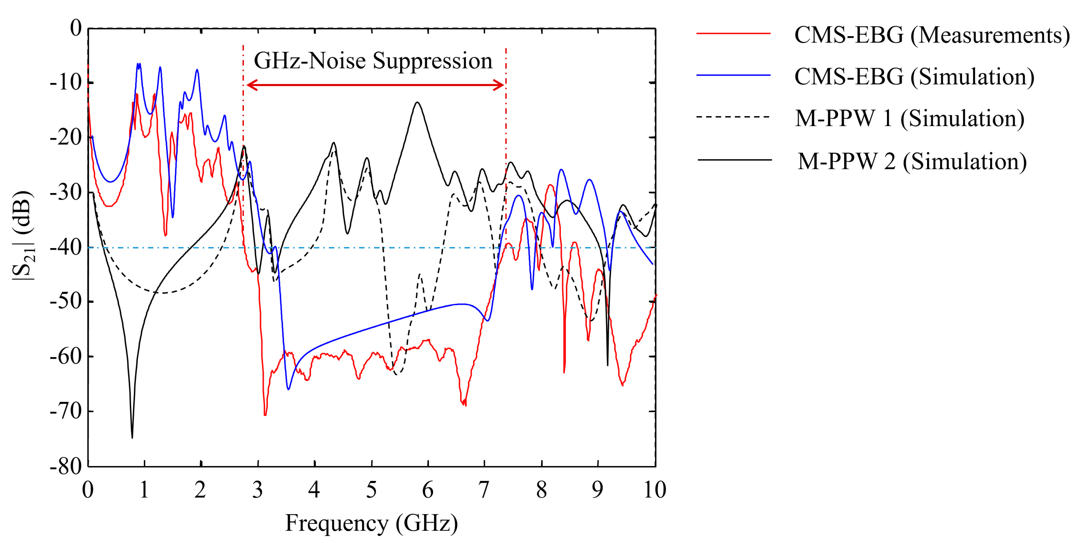
To compare the noise suppression characteristics of the CMS-EBG structure and the conventional PPW structure, the S21 parameter of the conventional structure is additionally extracted using the FEM simulation. The conventional structure is a multilayer PPW (M-PPW), which is a stack of PPWs. The layer assignment and via locations are identical to those in the CMS-EBG structure. The difference is that the M-PPW contains no EBG pattern and the VCA branch. Two types of port location are employed for the M-PPW: for M-PPW 1, the port location is equivalent to the CMS-EBG structure; for M-PPW 2, Port 1 consists of two terminals connected to the power plane in L3 and the ground plane in L4, and Port 2 is formed in the same layers. The port positions of M-PPW 1 and M-PPW 2 are identical; however, the layers of port 2 of M-PPW 1 and M-PPW 2 are different. The reason why M-PPW and the corresponding port configurations are chosen as compared structures is because they are widely used in MPCB applications.
The measured and simulated results of the noise suppression characteristics of the CMS-EBG structure are compared to the simulated results of M-PPW 1 and M-PPW 2 in Figure 10. It is seen that the electromagnetic noise in M-PPW 1 and M-PPW 2 can be significantly generated in the GHz frequency range considering the high level of resonant modes in the S21 parameter values. In contrast, the CMS-EBG structure suppresses the resonant modes and achieves a low level of S21 parameter in the GHz frequency range. In particular, the suppression level is below -40 dB in the frequency range from 2.7 GHz to 7.3 GHz. Thus, the CMS-EBG structure can substantially suppress the GHz electromagnetic noise in the wideband frequency range. The measured results of fL and fH show a good correlation with the predicted fL and fH by Floquet-Bloch analysis.
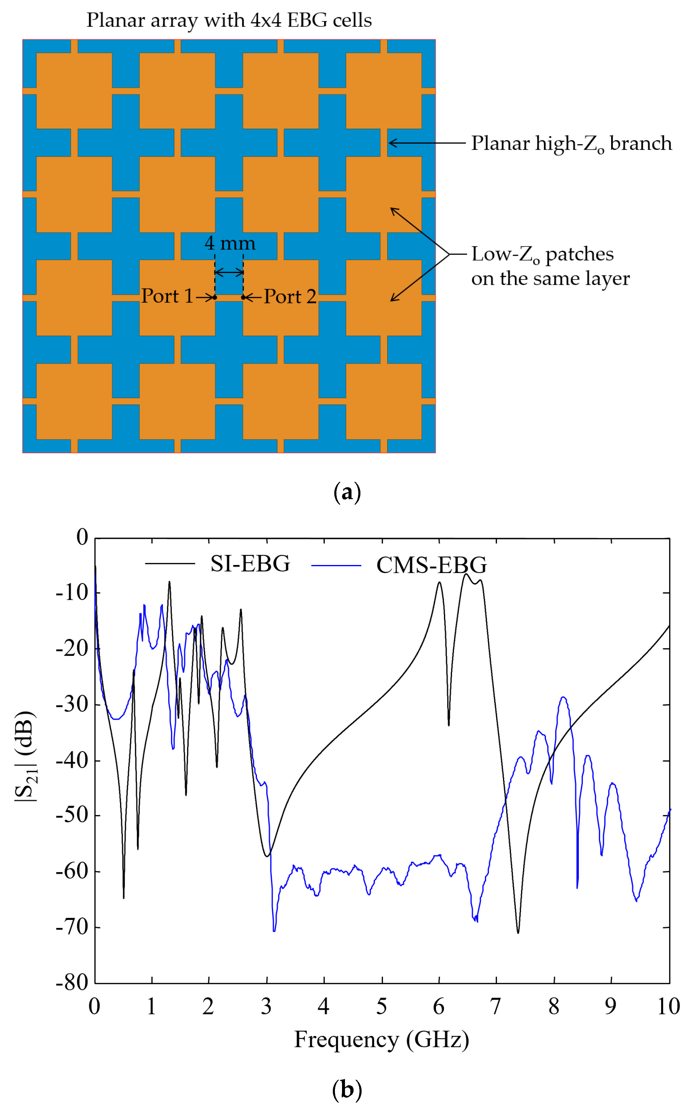
In addition to the wideband noise suppression, the CMS-EBG structure achieves a notably short distance between the noise source and the victim, which is less than the unit cell length. To prove the distinguished characteristics of the CMS-EBG structure, the noise suppression characteristics of the CMS-EBG structure and the previous stepped impedance EBG (SI-EBG) structure are compared. The previous SI-EBG structure [14] consists of 4-by-4 EBG cells with planar branches, as shown in Figure 11a. Its total number of the EBG cells are the same as that of the CMS-EBG structure. For the port configuration of the SI-EBG structure, the port distance is 4 mm in the unit cell. The measured result of the CMS-EBG structure is compared to the FEM simulation result of the SI-EBG structure in Figure 11b. A stopband of the SI-EBG structure is not clearly observed because its stopband is severely degraded. Thus, the SI-EBG structure with a short source-to-victim distance substantially reduces the noise suppression bandwidth and level. On the contrary, the CMS-EBG structure with a short distance substantially suppresses the GHz noise in the wideband frequency range.
In numerous MPCB applications, the planar area that the EBG structure occupies is more crucial than the number of layers that it uses. Moreover, a switching device (a noise source) is typically placed notably near the analog and wireless devices (noise victims) in the same MPCBs. The CMS-EBG structure achieves the wideband suppression of the GHz noise with a short source-to-victim distance and a compact area. In consequence, the CMS-EBG structure is the efficient solution for GHz noise suppression in such MPCB applications.
5. Conclusions
In this paper, the compact and multi-stack electromagnetic bandgap (CMS-EBG) structure was proposed for the suppression of the GHz noise in MPCBs. The noise suppression characteristics were predicted by Floquet-Bloch analysis with a derived dispersion equation and FEM simulation. Based on these methods, the design parameter effects were analyzed. The CMS-EBG structure was experimentally verified and compared to previous structures. The CMS-EBG structure shows the vastly superior characteristics compared to the previous structures. The main conclusions of this work are as follows:
- This paper proposes a multi-stack technique for the compact EBG structure in MPCBs. Sixteen EBG cells are efficiently arranged in the compact area of the 2 × 2 array size. The vertically stacked EBG patches are connected through the original configuration of the vertical branch. The consistent use of the vertical branch ensures good noise suppression and a simple analysis for the multi-stack EBG structure.
- The noise suppression characteristics of the CMS-EBG structure are predicted by applying the Floquet-Bloch analysis. To obtain the dispersion characteristics, the analytical equation based on the equivalent circuit model is derived, and the results are proven by comparison with the FEM simulation. For an example structure, the low- and high-cutoff frequencies are predicted as 1.98 GHz and 6.42 GHz, respectively. The CMS-EBG structure should significantly mitigate GHz noise in this frequency range. In addition, the main design parameter effect is thoroughly examined.
- From the measurements of the fabricated CMS-EBG structure in MPCBs, the low- and high-cutoff frequencies are 2.7 GHz and 7.3 GHz, which indicate a broad noise suppression region. The port distance is notably short (4 mm) and less than the unit cell length of 12 mm. The experimental results verify the distinguished noise suppression characteristics of the CMS-EBG structure with a compact size and a short source-to-victim distance.
Acknowledgments
This work was supported by Institute for Information & communications Technology Promotion (IITP) grant funded by the Korea government (MSIP) (No. 2016-0-00577, A Study on Core Technology for Multidimensional Immersive Media Broadcasting and Communication).
Author Contributions
Myunghoi Kim and Seungyoung Ahn conceived and designed the experiments; Myunghoi Kim analyzed the dispersion characteristics; Myunghoi Kim performed the simulations and experiments. Myunghoi Kim and Seungyoung Ahn wrote the paper.
Conflicts of Interest
The authors declare no conflict of interest.
References
- Swaminathan, M.; Kim, J.; Novak, I.; Libous, J.P. Power distribution networks for system-on-package: Status and challenges. IEEE Trans. Adv. Packag. 2004, 27, 286–300. [Google Scholar] [CrossRef]
- Li, E.P.; Wei, X.C.; Cangellaris, A.C.; Liu, E.X.; Zhang, Y.J.; D’Amore, M.; Kim, J.; Sudo, T. Progress Review of Electromagnetic Compatibility Analysis Technologies for Packages, Printed Circuit Boards, and Novel Interconnects. IEEE Trans. Electromagn. Compat. 2010, 52, 248–265. [Google Scholar]
- Swaminathan, M.; Chung, D.; Grivet-Talocia, S.; Bharath, K.; Laddha, V.; Xie, J. Designing and modeling for power integrity. IEEE Trans. Electromagn. Compat. 2010, 52, 288–310. [Google Scholar] [CrossRef]
- Wu, T.L.; Chuang, H.H.; Wang, T.K. Overview of power integrity solutions on package and PCB: Decoupling and EBG isolation. IEEE Trans. Electromagn. Compat. 2010, 52, 346–356. [Google Scholar] [CrossRef]
- Hwang, C.; Kim, J.; Achkir, B.; Fan, J. Analytical transfer functions relating power and ground voltage fluctuations to jitter at a single-ended full-swing buffer. IEEE Trans. Compon. Packag. Manuf. Technol. 2013, 3, 113–125. [Google Scholar] [CrossRef]
- Cui, W.; Fan, J.; Ren, Y.; Shi, H.; Drewniak, J.L.; DuBroff, R.E. DC power-bus noise isolation with power-plane segmentation. IEEE Trans. Electromagn. Compat. 2003, 45, 436–443. [Google Scholar] [CrossRef]
- Fan, J.; Drewniak, J.L.; Shi, H.; Knighten, J.L. DC power-bus modeling and design with a mixed-potential integral-equation formulation and circuit extraction. IEEE Trans. Electromagn. Compat. 2001, 43, 426–436. [Google Scholar] [CrossRef]
- Leone, M.; Friedrich, M.; Mantzke, A. Efficient broadband circuit-modeling approach for parallel-plane structures of arbitrary shape. IEEE Trans. Electromagn. Compat. 2013, 55, 941–948. [Google Scholar] [CrossRef]
- Zhang, M.S.; Tan, H.Z.; Mao, J.F. A novel layer stack-up with free cavity resonance for high-performance power noise suppression. IEEE Trans. Compon. Packag. Manuf. Technol. 2014, 4, 1973–1980. [Google Scholar] [CrossRef]
- Abhari, R.; Eleftheriades, G.V. Metallo-dielectric electromagnetic bandgap structures for suppression and isolation of the parallel-plate noise in high-speed circuits. IEEE Trans. Microw. Theory Tech. 2003, 51, 1629–1639. [Google Scholar] [CrossRef]
- Wu, T.Z.; Wang, C.C.; Lin, Y.H.; Wang, T.-K.; Chang, G. A novel power plane with super-wideband elimination of ground bounce noise on high speed circuits. IEEE Microw. Wirel. Compon. Lett. 2005, 15, 174–176. [Google Scholar]
- Wu, T.Z.; Lin, Y.H.; Wang, T.K.; Wang, C.C.; Chen, S.T. Electromagnetic bandgap power/ground planes for wideband suppression of ground bounce noise and radiated emission in high-speed circuits. IEEE Trans. Microw. Theory Tech. 2005, 53, 2935–2942. [Google Scholar]
- Kim, K.H.; Schutt-Aine, J.E. Design of EBG power distribution networks with VHF-B and cutoff frequency and small unit cell size for mixed-signal systems. IEEE Microw. Wirel. Compon. Lett. 2007, 17, 489–491. [Google Scholar] [CrossRef]
- Choi, J.; Govind, V.; Swaminathan, M.; Bharath, K. Noise isolation in mixed-signal systems using alternating impedance electromagnetic bandgap (AI-EBG) structure-based power distribution network (PDN). IEEE Trans. Adv. Packag. 2010, 33, 2–12. [Google Scholar] [CrossRef]
- Kim, M.; Koo, K.; Hwang, C.; Shim, Y.; Kim, J.; Kim, J. A compact and wideband electromagnetic bandgap structure using a defected ground structure for power/ground noise suppression in multilayer packages and PCBs. IEEE Trans. Electromagn. Compat. 2012, 54, 689–695. [Google Scholar]
- De Paulis, F.; Nisanci, M.H.; Orlandi, A. Practical EBG application to multilayer PCB: Impact on power integrity. IEEE Trans. Electromagn. Compat Mag. 2012, 1, 60–65. [Google Scholar] [CrossRef]
- Choi, J. Ultimate noise isolation in high-speed digital systems on packages and printed circuit boards. Electr. Lett. 2013, 49, 594–595. [Google Scholar] [CrossRef]
- Kim, M.; Koo, K.; Shim, Y.; Hwang, C.; Pak, J.S.; Ahn, S.; Kim, J. Vertical stepped impedance EBG (VSI-EBG) structure for wideband suppression of simultaneous switching noise in multilayer PCBs. IEEE Trans. Electromagn. Compat. 2013, 55, 307–314. [Google Scholar] [CrossRef]
- Kim, M.; Kam, D.G. A wideband and compact EBG structure with a circular defected ground structure. IEEE Trans. Compon. Packag. Manuf. Technol. 2014, 4, 496–503. [Google Scholar] [CrossRef]
- Kasahara, Y.; Toyao, H.; Hankui, E. Compact and multiband electromagnetic bandgap structures with adjustable bandgaps derived from branched open-circuit lines. IEEE Trans. Microw. Theory Tech. 2017, 65, 2330–2340. [Google Scholar] [CrossRef]
- Yoo, J.; Park, J.; Park, H.; Kim, J.; Shim, Y.; Song, T.; Kim, J. Analysis of the Vertical Electromagnetic Bandgap Structures in the Power Distribution Network for the Multi-layer Printed Circuit Board. In Proceedings of the 10th Electronics Packaging Technology Conference, Singapore, 9–12 December 2008; pp. 1381–1386. [Google Scholar]
- Shen, C.K.; Chen, C.H.; Han, D.H.; Wu, T.L. Modeling and analysis of bandwidth-enhanced multilayer 1-D EBG with bandgap aggregation for power noise suppression. IEEE Trans. Electromagn. Compat. 2015, 57, 858–867. [Google Scholar] [CrossRef]
- Wang, C.L.; Shiue, G.H.; Guo, W.D.; Wu, R.B. A systematic design to suppress wideband ground bounce noise in high-speed circuits by electromagnetic-bandgap-enhanced Split Powers. IEEE Trans. Microw. Theory Tech. 2006, 54, 4209–4217. [Google Scholar] [CrossRef]
- Wang, C.C.; Yu, Y.M.; de Paulis, F.; Scogna, A.C.; Orlandi, A.; Chiou, Y.P.; Wu, T.L. Bandwidth enhancement based on optimized via location for multiple vias EBG power/ground planes. IEEE Trans. Compon. Packag. Manuf. Technol. 2012, 2, 332–341. [Google Scholar] [CrossRef]
- Ansys, Inc. High Frequency Structure Simulator. Available online: http://www.ansys.com/ (accessed on 1 May 2017).
- Standard for Validation of Computational Electromagnetics Computer Modeling and Simulation—Part 1; IEEE: New York, NY, USA, 2008; p. P1597.1.
- Duffy, A.P.; Martin, A.J.M.; Orlandi, A.; Antonini, G.; Benson, T.M.; Woolfson, M.S. Feature Selective Validation (FSV) for validation of computational electromagnetics (CEM). Part I—The FSV method. IEEE Trans. Electromagn. Compat. 2006, 48, 449–459. [Google Scholar] [CrossRef]
- Orlandi, A.; Duffy, A.P.; Archambeault, B.; Antonini, G.; Coleby, D.E.; Connor, S. Feature Selective Validation (FSV) for validation of computational electromagnetics (CEM). Part II—Assessment of FSV performance. IEEE Trans. Electromagn. Compat 2006, 48, 460–467. [Google Scholar]
Figure 1.
Gigahertz (GHz)-noise suppression in multilayer printed circuit boards using electromagnetic bandgap structures and the limitations of previous planar electromagnetic bandgap (EBG) structures.
Figure 1.
Gigahertz (GHz)-noise suppression in multilayer printed circuit boards using electromagnetic bandgap structures and the limitations of previous planar electromagnetic bandgap (EBG) structures.

Figure 2.
(a) Illustration of the compact and multi-stack electromagnetic bandgap (CMS-EBG) structure with vertical-cell array (VCA) branches (the ground vias are not shown for simplicity) and (b) highlighted view of the patches and VCA branches of the power layers.
Figure 2.
(a) Illustration of the compact and multi-stack electromagnetic bandgap (CMS-EBG) structure with vertical-cell array (VCA) branches (the ground vias are not shown for simplicity) and (b) highlighted view of the patches and VCA branches of the power layers.
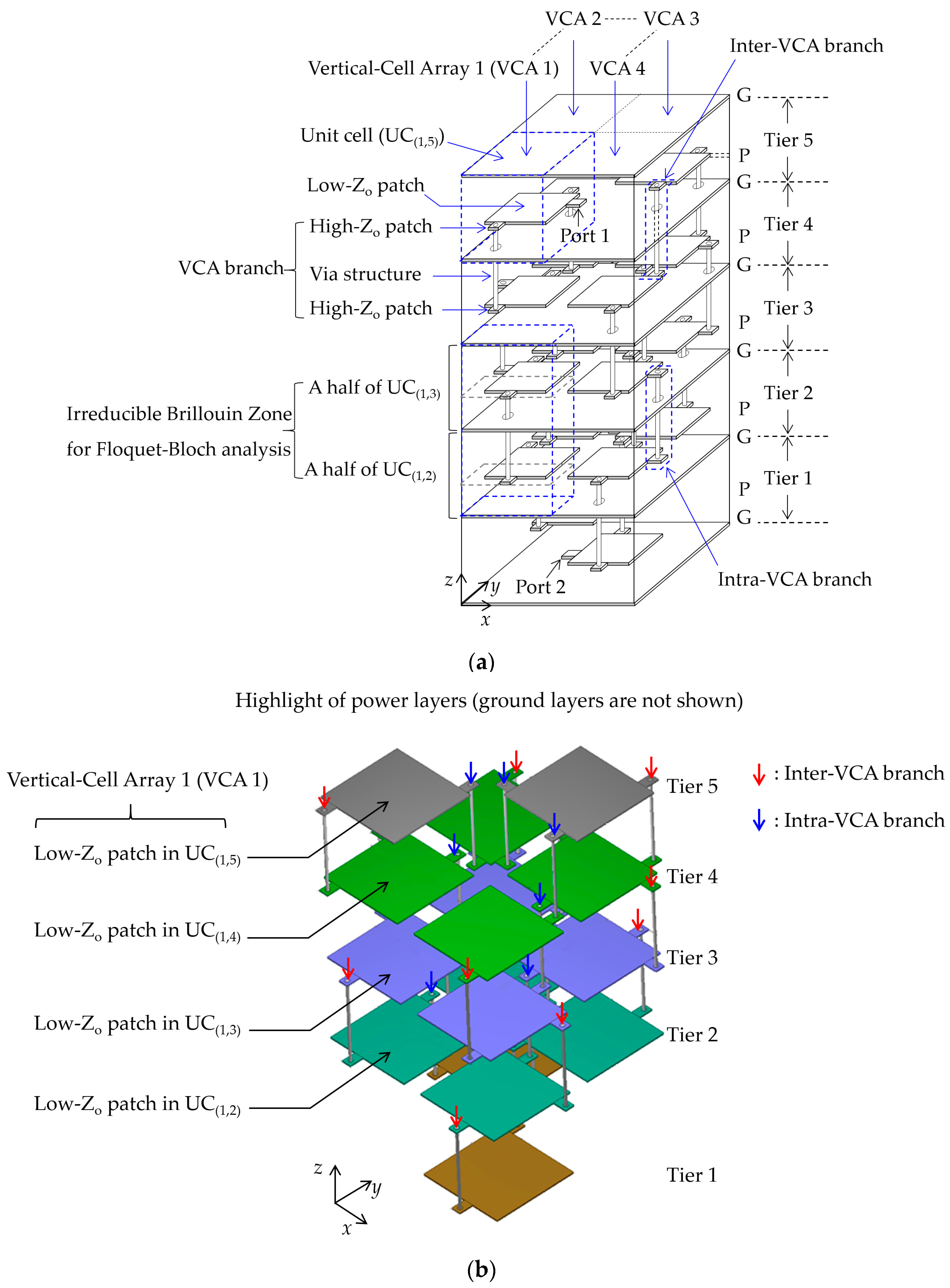
Figure 3.
A lattice diagram of the characteristic impedance of the CMS-EBG structure.

Figure 4.
(a) A unit cell with design parameters for Floquet-Bloch analysis and (b) an equivalent circuit model using a transmission line circuit to extract a dispersion equation.
Figure 4.
(a) A unit cell with design parameters for Floquet-Bloch analysis and (b) an equivalent circuit model using a transmission line circuit to extract a dispersion equation.

Figure 5.
Dispersion diagrams of the CMS-EBG structure from Floquet-Bloch analysis.
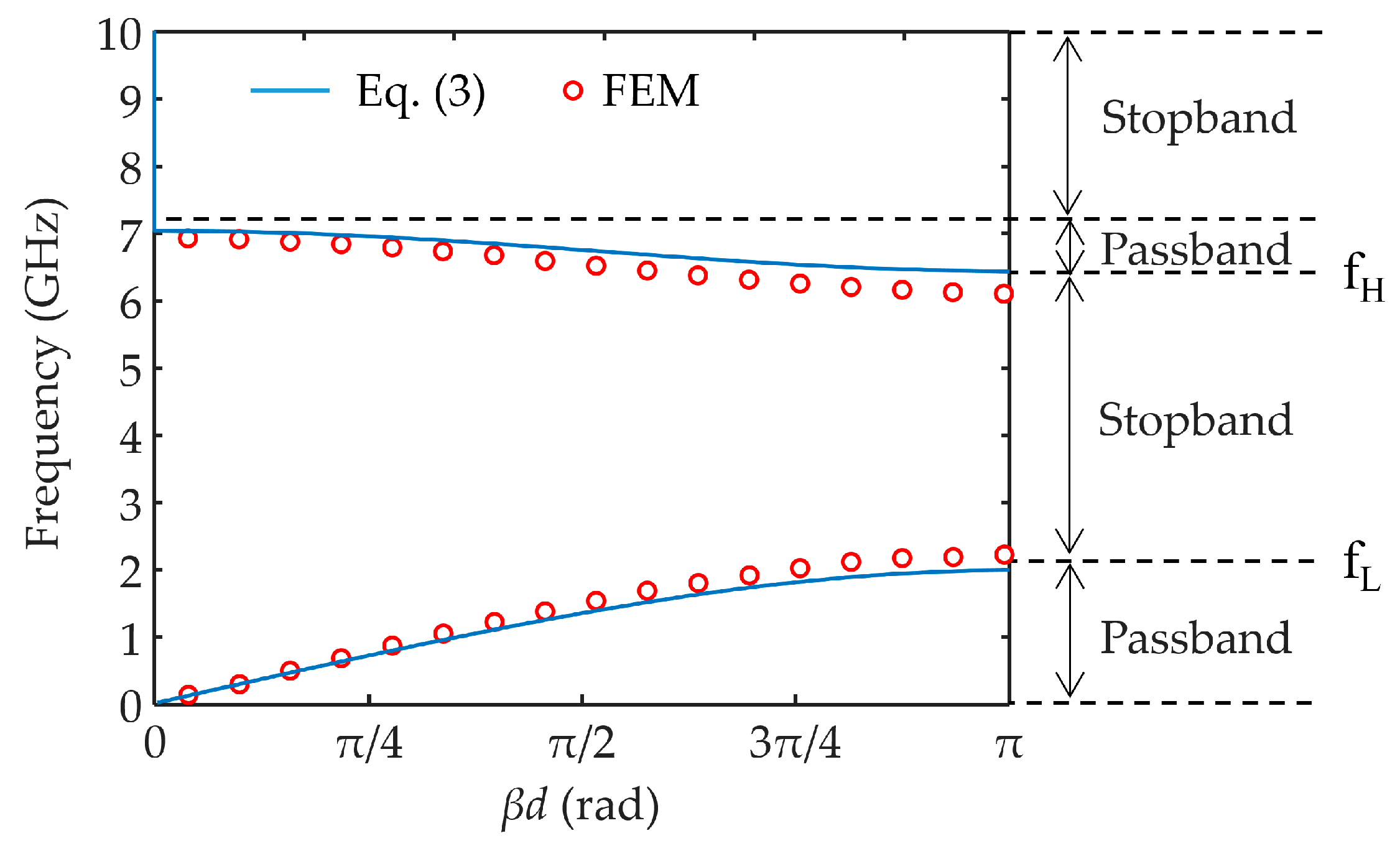
Figure 6.
Analysis of the wp effects on the low- and high-cutoff frequencies.

Figure 7.
Analysis of the wp effects on the (a) center frequency and (b) fractional bandwidth.
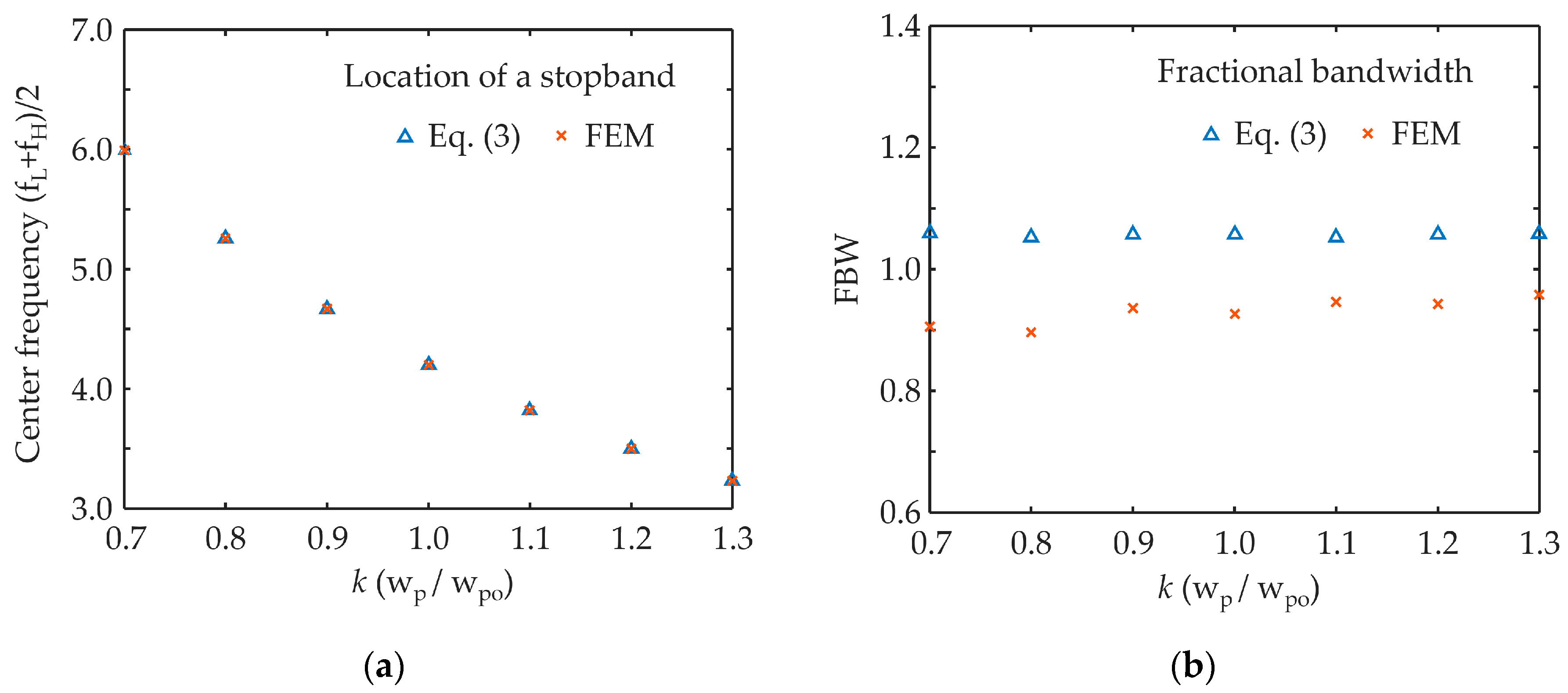
Figure 8.
A test vehicle of the CMS-EBG structure fabricated by the multilayer printed circuit board (MPCB) manufacturing process.
Figure 8.
A test vehicle of the CMS-EBG structure fabricated by the multilayer printed circuit board (MPCB) manufacturing process.

Figure 9.
Measurement setup for the noise suppression characteristics.
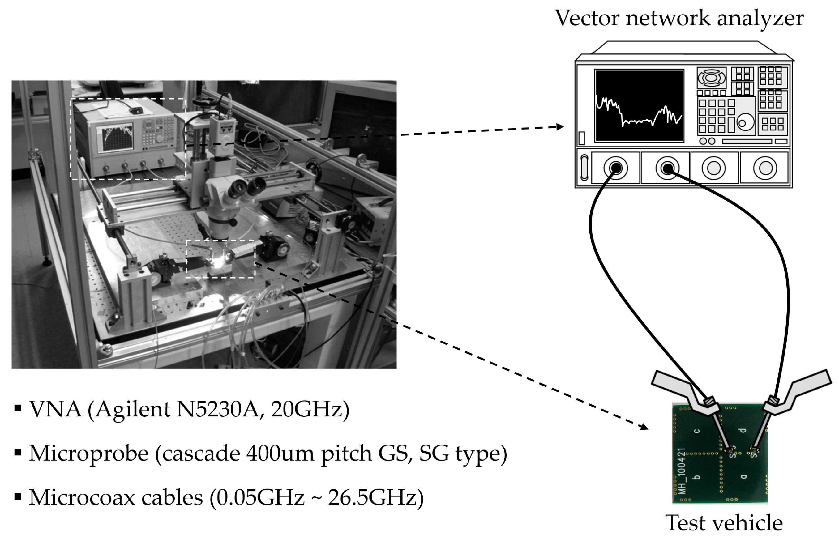
Figure 10.
Comparison of the noise suppression characteristics between the CMS-EBG structure and the conventional multilayer parallel plate waveguide (M-PPW) structures.
Figure 10.
Comparison of the noise suppression characteristics between the CMS-EBG structure and the conventional multilayer parallel plate waveguide (M-PPW) structures.

Figure 11.
(a) Finite-element method (FEM) simulation model of the previous stepped-impedance EBG (SI-EBG) structure and (b) comparison of the noise suppression characteristics between CMS-EBG and the SI-EBG structures.
Figure 11.
(a) Finite-element method (FEM) simulation model of the previous stepped-impedance EBG (SI-EBG) structure and (b) comparison of the noise suppression characteristics between CMS-EBG and the SI-EBG structures.


Table 1.
Summary of the design parameter effects on the low- and high-cutoff frequencies, center frequency, and fractional bandwidth.
Table 1.
Summary of the design parameter effects on the low- and high-cutoff frequencies, center frequency, and fractional bandwidth.
| Parameters | k (wp/wpo) | |||||||
|---|---|---|---|---|---|---|---|---|
| 0.7 | 0.8 | 0.9 | 1.0 | 1.1 | 1.2 | 1.3 | ||
| ZoL (Ω) | 1.16 | 1.03 | 0.90 | 0.82 | 0.75 | 0.68 | 0.62 | |
| Equation (3) (GHz) | fL | 2.82 | 2.49 | 2.20 | 1.98 | 1.81 | 1.65 | 1.52 |
| fH | 9.17 | 8.02 | 7.13 | 6.42 | 5.83 | 5.35 | 4.94 | |
| fC 1 | 6.00 | 5.23 | 4.67 | 4.20 | 3.82 | 3.50 | 3.23 | |
| FBW 2 | 1.06 | 1.05 | 1.06 | 1.06 | 1.05 | 1.06 | 1.06 | |
| FEM (GHz) | fL | 3.2 | 2.85 | 2.47 | 2.24 | 2.02 | 1.85 | 1.68 |
| fH | 8.49 | 7.48 | 6.81 | 6.11 | 5.65 | 5.15 | 4.77 | |
| fC | 5.85 | 5.17 | 4.64 | 4.18 | 3.84 | 3.50 | 3.23 | |
| FBW | 0.91 | 0.90 | 0.94 | 0.93 | 0.95 | 0.94 | 0.96 | |
1 Center frequency: (fH + fL)/2; 2 Fractional bandwidth: (fH − fL)/fC.
© 2017 by the authors. Licensee MDPI, Basel, Switzerland. This article is an open access article distributed under the terms and conditions of the Creative Commons Attribution (CC BY) license (http://creativecommons.org/licenses/by/4.0/).
Share and Cite
MDPI and ACS Style
Kim, M.; Ahn, S. A Compact and Multi-Stack Electromagnetic Bandgap Structure for Gigahertz Noise Suppression in Multilayer Printed Circuit Boards. Appl. Sci. 2017, 7, 804. https://doi.org/10.3390/app7080804
AMA Style
Kim M, Ahn S. A Compact and Multi-Stack Electromagnetic Bandgap Structure for Gigahertz Noise Suppression in Multilayer Printed Circuit Boards. Applied Sciences. 2017; 7(8):804. https://doi.org/10.3390/app7080804
Chicago/Turabian StyleKim, Myunghoi, and Seungyoung Ahn. 2017. "A Compact and Multi-Stack Electromagnetic Bandgap Structure for Gigahertz Noise Suppression in Multilayer Printed Circuit Boards" Applied Sciences 7, no. 8: 804. https://doi.org/10.3390/app7080804
Note that from the first issue of 2016, this journal uses article numbers instead of page numbers. See further details here.