
High Conductivity and Adhesion of Cu-Cr-Zr Alloy for TFT Gate Electrode
by
 , , , and
Junbiao Peng
1, 
Kuankuan Lu
1,
Shiben Hu
1 ,
,
Zhiqiang Fang
1,
Honglong Ning
1,*,
Jinglin Wei
1,
Zhennan Zhu
1,
Yicong Zhou
1,
Lei Wang
1,
Rihui Yao
1,* and
Xubing Lu
2 1
Institute of Polymer Optoelectronic Materials and Devices, State Key Laboratory of Luminescent Materials and Devices, South China University of Technology, Guangzhou 510640, China
2
Institute for Advanced Materials and Guangdong Provincial Key Laboratory of Quantum Engineering and Quantum Materials, South China Normal University, Guangzhou 510006, China
*
Authors to whom correspondence should be addressed.
Appl. Sci. 2017, 7(8), 820; https://doi.org/10.3390/app7080820
Submission received: 10 June 2017
/
Revised: 22 July 2017
/
Accepted: 7 August 2017
/
Published: 10 August 2017
(This article belongs to the Special Issue Thin-Film Transistor)
Abstract
:The characteristics of Cu alloy (0.3 wt. % Cr, 0.2 wt. % Zr) thin film deposited by direct current (DC) magnetron sputtering deposition were investigated. The conductivity and adhesion of the Cu-0.3%Cr-0.2%Zr films were optimized by increasing the sputter power to 150 W and reducing the sputter pressure to 2 mTorr. With an annealing process (at 300 °C for 1 h in argon ambient atmosphere), the resistivity of the alloy film decreased from 4.80 to 2.96 μΩ·cm, and the adhesion classification increased from 2B to 4B on glass substrate. X-ray photoelectron spectroscopy (XPS) analysis showed that Cr aggregated toward the surface of the film and formed a self-protection layer in the annealing process. Transmission electron microscopy (TEM) indicated the aggregation and migration of Cr in the annealing process. A further X-ray diffraction (XRD) analysis showed that Cu2O appeared when the annealing temperature reached above 350 °C, which accounts for the increase of the resistivity. Based on Al2O3 and SiO2 substrate surfaces, the Cu-0.3%Cr-0.2%Zr film also showed high conductivity and adhesion, which has a potential in the application of Cu gate electrodes for thin film transistor (TFT).
1. Introduction
As the large-size and high-resolution thin-film transistor liquid crystal display (TFT-LCD) with high operating frequency becomes more widely used, the copper gate electrode is a promising candidate to substitute for aluminum, owing to its high conductivity to reduce the resistance-capacitance (RC) propagation delay as well as its higher stress-migration and electromigration resistance [1]. However, before it can be used for this purpose, copper has a serious drawback to be addressed, as it is well-known to exhibit poor adhesion to substrates such as SiO2 or glass [2,3,4]. Another challenge in Cu gate electrode technology is how to prevent the diffusion of Cu into neighbor layers under bias, as Cu tends to degrade the dielectric properties of the neighbor layer, resulting in dielectric breakdown and inferior device performance [5,6,7].
Several methods are proposed to resolve this problem, by introducing an extra layer at the interface as a diffusion barrier and adhesion layer, such as Cu/Ti [8,9], Cu/Ta [10], Cu/Mn [11], or Cu/Mo [12,13]. However, the extra functional layer gives rise to a complex pattern process. The differences between the Cu layer and the contact layer make it complicated in the subsequent etching process [14]. In order to improve the reliability and cost of Cu gate electrodes, another method is advocated, namely, the use of Cu alloy (Cu-Mg [15,16], Cu-Ca [17,18,19], Cu-Mn [20,21,22,23], Cu-Ti [24]) instead of pure Cu to form a diffusion barrier and adhesion layer spontaneously [25].
In this paper, we focus on the ternary alloy thin film of Cu-0.3 wt. %Cr-0.2 wt. %Zr (Cu-Cr-Zr). The additive elements of Cr and Zr have limited solid solubility in Cu alloy, and thus will migrate to the interface and be oxidized by the surface oxide layer during subsequent annealing, acting as a self-forming diffusion barrier and adhesion layer [21]. The simultaneous presence of Cr and Zr—two additive elements—results in a higher diffusion coefficient and provides higher conductivity and adhesion than only one. Therefore, the properties of Cu-Cr-Zr thin film were investigated in view of their electronic properties and adhesion, aiming at developing the application of Cu gate electrodes in TFT.
2. Materials and Methods
Thin films of Cu-Cr-Zr were deposited on alkali-free glass substrates by direct current (DC) magnetron sputtering. Prior to deposition, the substrates were first cleaned for 10 min by ultrasonication with deionized water and isopropanol, respectively. The distance between the targets and substrates was set to be 10 cm. The base pressure in the vacuum chamber was 5 × 10⁻⁴ Pa; the sputtering power was set at different levels (50 W, 150 W), as well as the argon (Ar) working pressure (2 mTorr and 20 mTorr), which aimed to evaluate the effect of sputtering power and sputtering pressure on the electronic resistivity and adhesion strength by combining experimental parameters with Minitab software, so as to find the optimal parameters for the deposition of thin films. No intentional cooling or heating of the substrates was provided during the deposition. After the deposition, the film thickness was determined by a Veeco Dektak 150 probe surface profiler. The thickness was then fixed at 200 nm, which was controlled by the deposition time under different sputter rates. The sheet resistance was measured by using a four-point probe. Furthermore, the resistance was calculated by the following formula:
where ρ, Rs, and t are defined as the specific resistance, the film sheet resistance, and the film thickness, respectively. Different substrates were carried out in the same way. The sputter power and sputter pressure was fixed at 150 W and 2 mTorr, respectively. The Ar flow was fixed at 25 sccm. Table 1 shows the detailed parameters of these substrates:
The thin film adhesion strength was measured by means of the standard test methods for measuring adhesion (i.e., American Society for Testing and Materials (ASTM) D3359) [26] with the pressure-sensitive tape, and then classified as one of six grades (5B, 4B, 3B, 2B, 1B, and 0B) according to the area percentage of the removal of coating from the substrate after scratching. 5B indicates no coating removal, indicating optimal adhesion. Table 2 shows the classification of adhesion test results.
The annealing process was conducted in a vacuum annealing furnace with the protection of Ar atmosphere. The Ar flow was set to 110 sccm; the annealing pressure was set to 1 Torr; the annealing time was set to 1 h; the annealing temperatures were set to 300 °C, 350 °C, 400 °C, and 450 °C. The crystalline structure of thin films was determined by X-ray diffraction (XRD) measurement using Cu Kα1 radiation (λ = 0.15418 nm). XRD measurement was performed by an Empyrean Nano edition (PANalytical, Almelo, The Netherlands). The chemical changes in the surface of the films were detected by X-ray photoelectron spectroscopy (XPS) measurements. XPS measurement was performed by an ESCALAB250Xi (Thermo Fisher Scientific, Waltham, MA, USA) at a basic pressure of 7.5 × 10⁻¹⁰ Torr. SEM measurement was performed by a Nova Nano SEM (FEI, Hillsboro, OR, USA).
3. Results and Discussions
3.1. Resistivity
Figure 1 shows the main effects plot (a) and interaction plot (b) of the parameters such as sputter power, sputter pressure, and annealing temperature. It shows that the resistivity of Cu-Cr-Zr thin film is effected more or less by all the three factors: sputter power, sputter pressure, and annealing temperature.
As shown in Figure 1a, both the power and the pressure act as major effects, and when the temperature is in the range of 300–400 °C, there is little effect, but once exceeding 400 °C, the annealing temperature becomes the main effect factor of the resistance value.
Further analysis shows that higher sputter power and lower sputter pressure will induce a lower resistivity; annealing in a certain range of temperature is advantageous in reducing the resistivity, while too high of an annealing temperature will lead to the opposite effect. When the effect of a factor depends on the quasi-level of another one, the interaction plot can be used to show the interaction between the two factors. The greater the slope difference between lines, the greater the degree of interaction. As shown in Figure 1b, the factors of sputtering power and sputtering pressure interact with each other, but the annealing temperature has little interaction with them. This is reasonable, as the factors of power and pressure work during sputtering deposition at the same time, while annealing is a separate factor that affects the film during post-processing. Thus, we fixed the optimal deposition conditions of the film at 150 W, 2 mTorr, and all the experiments below follow this condition.
Figure 2a shows the resistivity of pure Cu thin films on different substrates with annealing temperatures of 300 °C, 350 °C, 400 °C, and 450 °C. Figure 2b shows the resistivity of Cu-Cr-Zr thin films on different substrates with annealing temperatures of 300 °C, 350 °C, 400 °C, and 450 °C. We learned that an annealing process at 300 °C leads to the best optimized resistivity for Cu-Cr-Zr, which is presumably caused by the reduction of the defect density of the Cu lattice and the increase in grain size to reduce electron scattering at grain boundaries. When the annealing temperature exceeds 400 °C, the resistivity rises sharply, which indicates that the electrical characteristics of the Cu alloy film deteriorate abruptly.
3.2. Adhesion
Figure 3a shows the effects of annealing temperature on the adhesion of pure Cu thin films on various substrates; Figure 3b shows the effects of annealing temperature on the adhesion of Cu-Cr-Zr thin films on various substrates. For pure Cu, adhesion strength is very inferior with glass, although its resistivity is lower than Cu-Cr-Zr, as shown in Figure 2. For Cu-Cr-Zr, the strength of adhesion increases after annealing at 300 °C or higher for all of the substrates, reaching almost 0% peeling rate on all substrates, as shown in Figure 3. The adhesion grades of Cu-Cr-Zr thin film on various substrates are shown in Table 3. The adhesion grade varies from 2B to 4B for the as-deposited Cu-Cr-Zr film, and even with no annealing process the adhesion strength was better than that of pure Cu thin film, which was graded at 0B.
3.3. X-ray Photoelectron Spectroscopy (XPS) Results
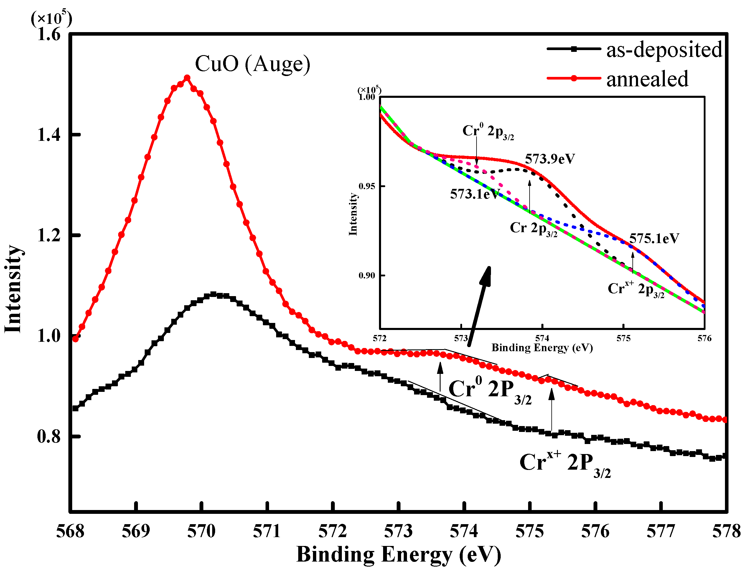
Figure 4 shows the XPS spectra of Cr2p core levels on the Cu-Cr-Zr thin film surface before and after annealing at 300 °C. The intensity of Cr2p signals for the annealed sample is stronger than that for the as-deposited sample, but the signal at 574 eV is still weak because of the tiny amount of Cr. This is attributed to the low solid solubility of chromium in Cu, which can easily migrate toward the interface and react to form an oxide layer with the annealing process. The oxide layer enhances the oxidation resistance of Cu in air. Another added metal element in the Cu alloy is zirconium, which exhibits the same function as Cr but at a concentration too small to be detected.
3.4. Transmission Electron Microscopy (TEM) Results
Figure 5 shows the cross-section of Cu-Cr-Zr/Glass samples as-deposited and after annealing at 300 °C. For the as-deposited sample shown in Figure 5a, the film surface is smooth. In contrast, the sample annealed at a temperature of 350 °C exhibited some particles in the surface, as arrow A shown in Figure 5b, indicating the accumulation of Cr on the surface, as evidenced in Figure 4. It may be speculated that there is also some Cr or Zr enrichment at the interface. The improvement of adhesion is ascribed to the aggregation of Cr and Zr in the surface and interface.
3.5. X-ray Diffraction Results
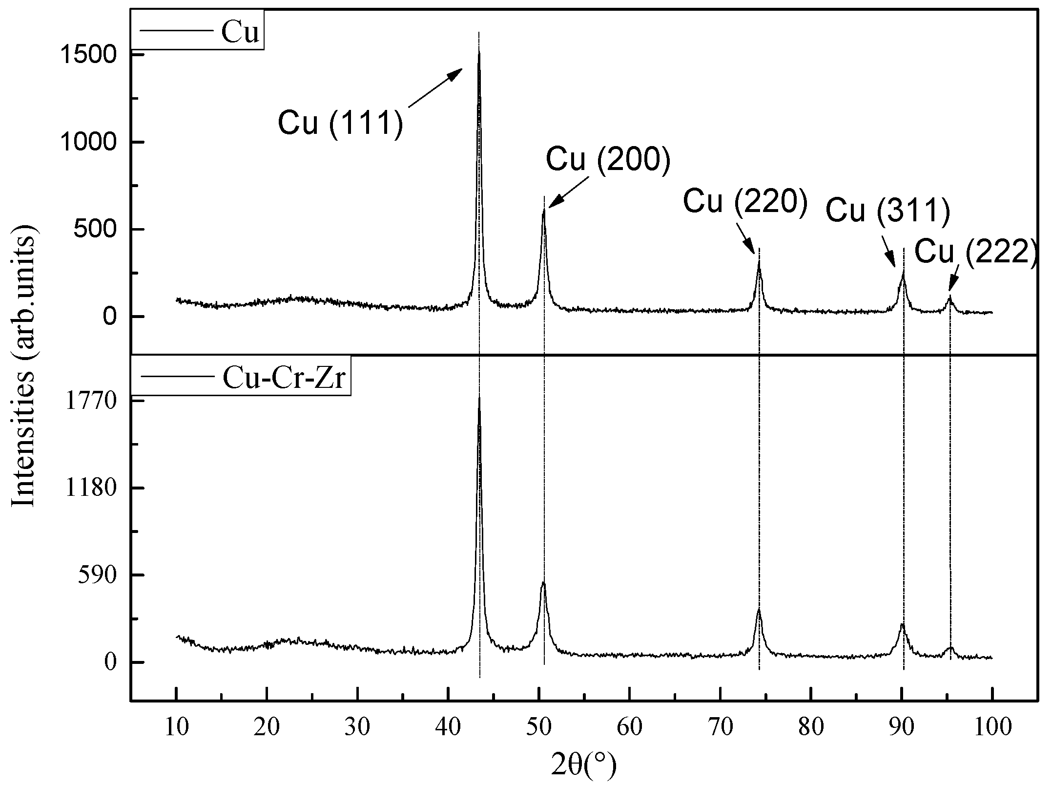
Figure 6 shows the XRD photos of Cu-Cr-Zr and pure Cu thin-film samples manufactured in the same way. It indicates that the other two elements of Cr and Zr almost have no effect on the crystal structure of the Cu film, which accounts for the relatively low resistivity of Cu-Cr-Zr thin films.
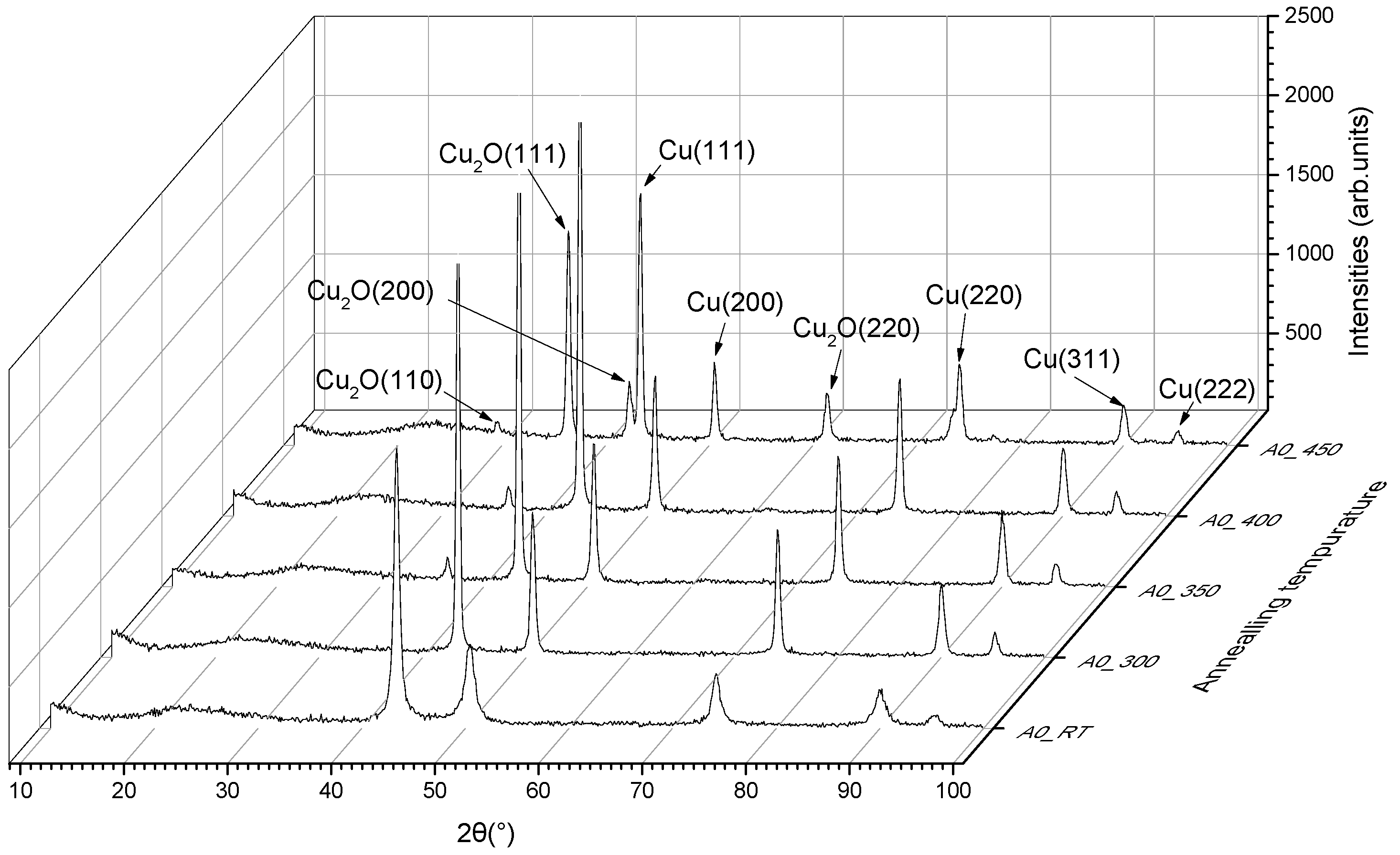
Figure 7 shows the X-ray diffraction patterns of Cu-Cr-Zr thin-film samples after annealing at various temperatures. As a comparison, the X-ray diffraction pattern of the as-deposited thin-film sample is also included. As shown in the figure, all the samples exhibit five peaks at 2θ values of 43.45°, 50.55°, 74.25°, 90.05°, and 95.25°, corresponding to Cu (111), (200), (220), (311), and (222) diffraction peaks, respectively, and grow along the Cu (111) preferential orientation. The preferential orientation is Cu (111) because copper, as a face-centered cubic (fcc) crystal, has the maximum atomic density and the least surface energy in the crystal indices, which is beneficial to the growth of the crystal face. In addition, with the annealing process, the Cu peak intensities are strengthened evidently and the Cu peaks become narrower, which indicates grain growth and the densification of the Cu film [17]. The Cu crystallinity becomes better as the annealing temperature increases, but when the temperature exceeds 400 °C, the Cu peak intensities become a little weaker, with some new Cu2O peaks appearing. It is worth noting that a Cu2O (111) peak appears when the annealing temperature exceeds 350 °C, which explains the very slight increase in resistivity, as shown in Figure 2. In addition, at 450 °C some peaks such as Cu2O (110), Cu2O (200), and Cu2O (220) appear and the Cu2O (111) peak intensity increases dramatically, resulting in the rapid deterioration of the membrane resistivity.
4. Conclusions
Cu-0.3 wt. % Cr-0.2 wt. % Zr alloy thin films deposited by a sputtering technique exhibit a smooth surface on glass substrate with a high sputter power and a low sputter pressure. After annealing at 300–400 °C, with large lateral grown grains, the Cu alloy film exhibits superior low resistivity and high adhesion on different kinds of substrates. X-ray diffraction (XRD) shows obvious grain growth after annealing, which accounts for the decrease of the resistivity. X-ray photoelectron spectroscopy (XPS) shows the migration of Cr toward the film surface, which enhances the oxidation resistance of Cu in air.
Acknowledgments
This work was supported by NSFC (No. U1601651), National Key R & D Program of China (No. 2016YFB0401504), National Key Basic Research and Development Program of China (973 program, Grant No. 2015CB655004) founded by MOST, Guangdong Natural Science Foundation (2016A030313459), Science and Technology Project of Guangdong Province (2014B090915004, 2015A010101323 and 2016B090907001), the Fundamental Research Funds for the Central Universities (2015ZP024 and 2015ZZ063), and the Project for Guangdong Province Universities and Colleges Pearl River Scholar Funded Scheme (2016).
Author Contributions
Junbiao Peng and Kuankuan Lu wrote the main manuscript text. Shiben Hu, Zhiqiang Fang, Honglong Ning and Jinglin Wei organized the data and drew the figures. Zhennan Zhu, Yicong Zhou and Lei Wang searched the literatures. The project was guided by Rihui Yao and Xubing Lu, who provided suggestions on content and structure.
Conflicts of Interest
The authors declare no conflicts of interest.
References
- Murarka, S.P.; Hymes, S.W. Copper metallization for ULSL and beyond. Crit. Rev. Solid State Mater. Sci. 1995, 20, 87–124. [Google Scholar] [CrossRef]
- Seah, C.H.; Mridha, S. Adhesive strength of electroplated copper films. J. Mater. Process. Technol. 2001, 114, 252–256. [Google Scholar] [CrossRef]
- Lee, B.S.; Lee, I. A study on the galvanic reaction between Cu and Mo as well as MoW for TFT-LCDs by using a zero-Resistance ammeter. SID Symp. Dig. Tech. Pap. 2009, 40, 1320–1323. [Google Scholar] [CrossRef]
- Nagao, K.; Neaton, J.B. First-principles study of adhesion at Cu/SiO2 interfaces. Phys. Rev. B 2003, 68, 1–9. [Google Scholar] [CrossRef]
- Mcbrayer, J.D.; Swanson, R.M. Diffusion of Metals in Silicon Dioxide. J. Electrochem. Soc. 1986, 133, 1242–1246. [Google Scholar] [CrossRef]
- Igarashi, Y.; Yamanobe, T. Thermal stability of copper interconnects fabricated by dry-etching process. Thin Solid Films 1995, 262, 124–128. [Google Scholar] [CrossRef]
- Hwang, S.; Jung, S. The electric field dependence of Cu migration induced dielectric failure in interlayer dielectric for integrated circuits. J. Appl. Phys. 2007, 101, 074501. [Google Scholar] [CrossRef]
- Park, J.S.; Kim, T.S. Ti/Cu bilayer electrodes for SiNx-passivated Hf-In-Zn-O thin film transistors: Device performance and contact resistance. Appl. Phys. Lett. 2010, 97, 162105. [Google Scholar] [CrossRef]
- Lee, Y.W.; Kim, S. Effect of Ti/Cu Source/Drain on an Amorphous IGZO TFT Employing SiNx Passivation for Low Data-Line Resistance. Electrochem. Solid State Lett. 2012, 15, H126–H129. [Google Scholar] [CrossRef]
- Ahrens, C.; Depta, D. Electrical characterization of conductive and non-conductive barrier layers for Cu-metallization. Appl. Surf. Sci. 1995, 91, 285–290. [Google Scholar] [CrossRef]
- Yun, P.S.; Koike, J. Metal Reaction Doping and Ohmic Contact with Cu-Mn Electrode on Amorphous In-Ga-Zn-O Semiconductor. J. Electrochem. Soc. 2011, 158, H1034–H1040. [Google Scholar] [CrossRef]
- Liu, K.; Chang, T. Investigation of channel width-dependent threshold voltage variation in a-InGaZnO thin-film transistors. Appl. Phys. Lett. 2014, 104, 133503. [Google Scholar] [CrossRef]
- Seo, B.; Lee, S. Effect of nitric acid on wet etching behavior of Cu/Mo for TFT application. Curr. Appl. Phys. 2011, 11, S262–S265. [Google Scholar] [CrossRef]
- Kim, H.; Koseki, T. Cu Wettability and Diffusion Barrier Property of Ru Thin Film for Cu Metallization. J. Electrochem. Soc. 2005, 152, G594–G600. [Google Scholar] [CrossRef]
- Wang, M.; Chang, T.C. Cu/CuMg Gate Electrode for the Application of Hydrogenated Amorphous Silicon Thin-Film Transistors. Electrochem. Solid State Lett. 2007, 10, J83–J85. [Google Scholar] [CrossRef]
- Wang, M.; Chang, T.C. Suppression of Schottky leakage current in island-in amorphous silicon thin film transistors with the Cu/CuMg as source/drain metal. Appl. Phys. Lett. 2007, 91, 062103. [Google Scholar] [CrossRef]
- Yu, Z.; Ren, R. The role of oxygen in the deposition of copper-calcium thin film as diffusion barrier for copper metallization. Appl. Surf. Sci. 2015, 328, 374–379. [Google Scholar] [CrossRef]
- Mori, S.; Kawai, A. Low-Resistivity and Adhesive Sputter-Deposited Cu-Ca Films with an Intermediate Oxide Layer. Jpn. J. Appl. Phys. 2010, 49, 075804. [Google Scholar] [CrossRef]
- Takasawa, S.; Ishibashi, S. Lower Resistivity Wiring Process for TFT Source/Drain Electrodes by Oxygen-Mixture Sputtering of Cu-Ca Alloy. SID Symp. Dig. Tech. Pap. 2009, 40, 1313–1316. [Google Scholar] [CrossRef]
- Koike, J.; Wada, M. Self-forming diffusion barrier layer in Cu-Mn alloy metallization. Appl. Phys. Lett. 2005, 87, 041911. [Google Scholar] [CrossRef]
- Haneda, M.; Iijima, J. Growth behavior of self-formed barrier at Cu-Mn/SiO2 interface at 250–450 °C. Appl. Phys. Lett. 2007, 90, 252107. [Google Scholar] [CrossRef]
- Lozano, J.; Lozanoperez, S. Interdiffusion and barrier layer formation in thermally evaporated Mn/Cu heterostructures on SiO2 substrates. Appl. Phys. Lett. 2011, 98, 123112. [Google Scholar] [CrossRef]
- Koike, J.; Hirota, K. Cu-Mn Electrodes for a-Si TFT and Its Electrical Characteristics. SID Symp. Dig. Tech. Pap. 2010, 41, 1343–1346. [Google Scholar] [CrossRef]
- Tsukimoto, S.; Kabe, T. Effect of Annealing Ambient on the Self-Formation Mechanism of Diffusion Barrier Layers Used in Cu(Ti) Interconnects. J. Electron. Mater. 2007, 36, 258–265. [Google Scholar] [CrossRef]
- Ding, P.J.; Lanford, W. Oxidation resistant high conductivity copper films. Appl. Phys. Lett. 1994, 64, 2897–2899. [Google Scholar] [CrossRef]
- ASTM D 3359. Standard Test Methods for Measuring Adhesion by Tape Test. Available online: http://www.astm.org/cgi-bin/resolver.cgi?D3359 (accessed on 9 August 2017).
Figure 1.
(a) Main effects plot and (b) interaction plot for the resistivity of Cu-Cr-Zr thin films affected by sputter power, sputter pressure, and annealing temperature.
Figure 1.
(a) Main effects plot and (b) interaction plot for the resistivity of Cu-Cr-Zr thin films affected by sputter power, sputter pressure, and annealing temperature.
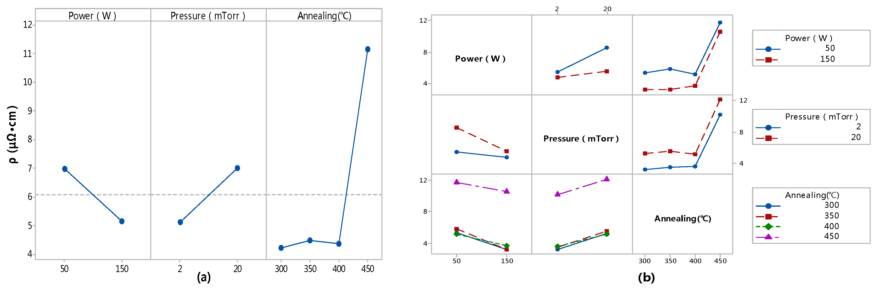
Figure 2.
Resistivity on different substrates with different annealing temperatures: (a) Pure Cu; (b) Cu-Cr-Zr.
Figure 2.
Resistivity on different substrates with different annealing temperatures: (a) Pure Cu; (b) Cu-Cr-Zr.
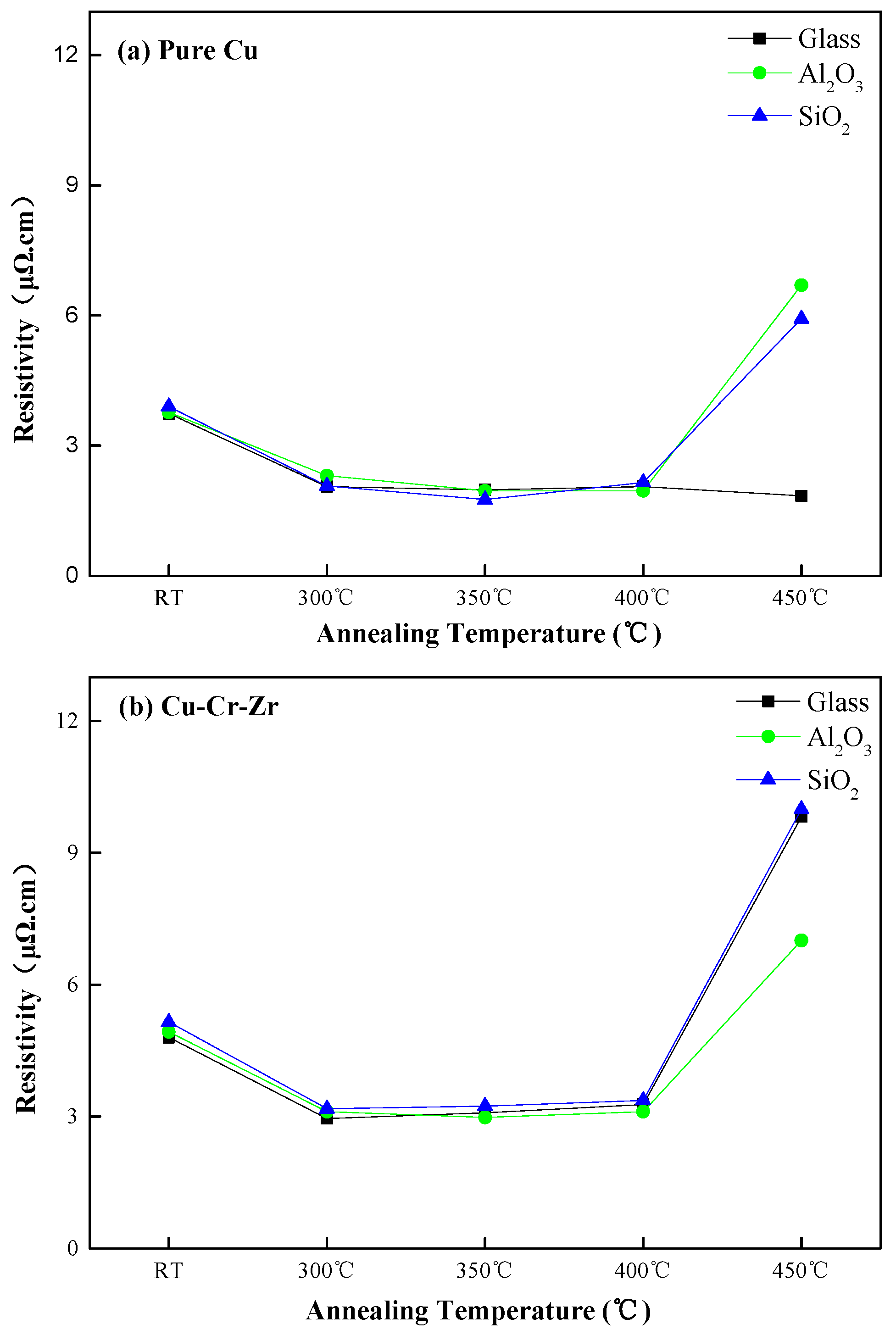
Figure 3.
Adhesion on various substrates at different annealing temperatures with the contrast of Cu/Ti on glass: (a) pure Cu; (b) Cu-Cr-Zr.
Figure 3.
Adhesion on various substrates at different annealing temperatures with the contrast of Cu/Ti on glass: (a) pure Cu; (b) Cu-Cr-Zr.
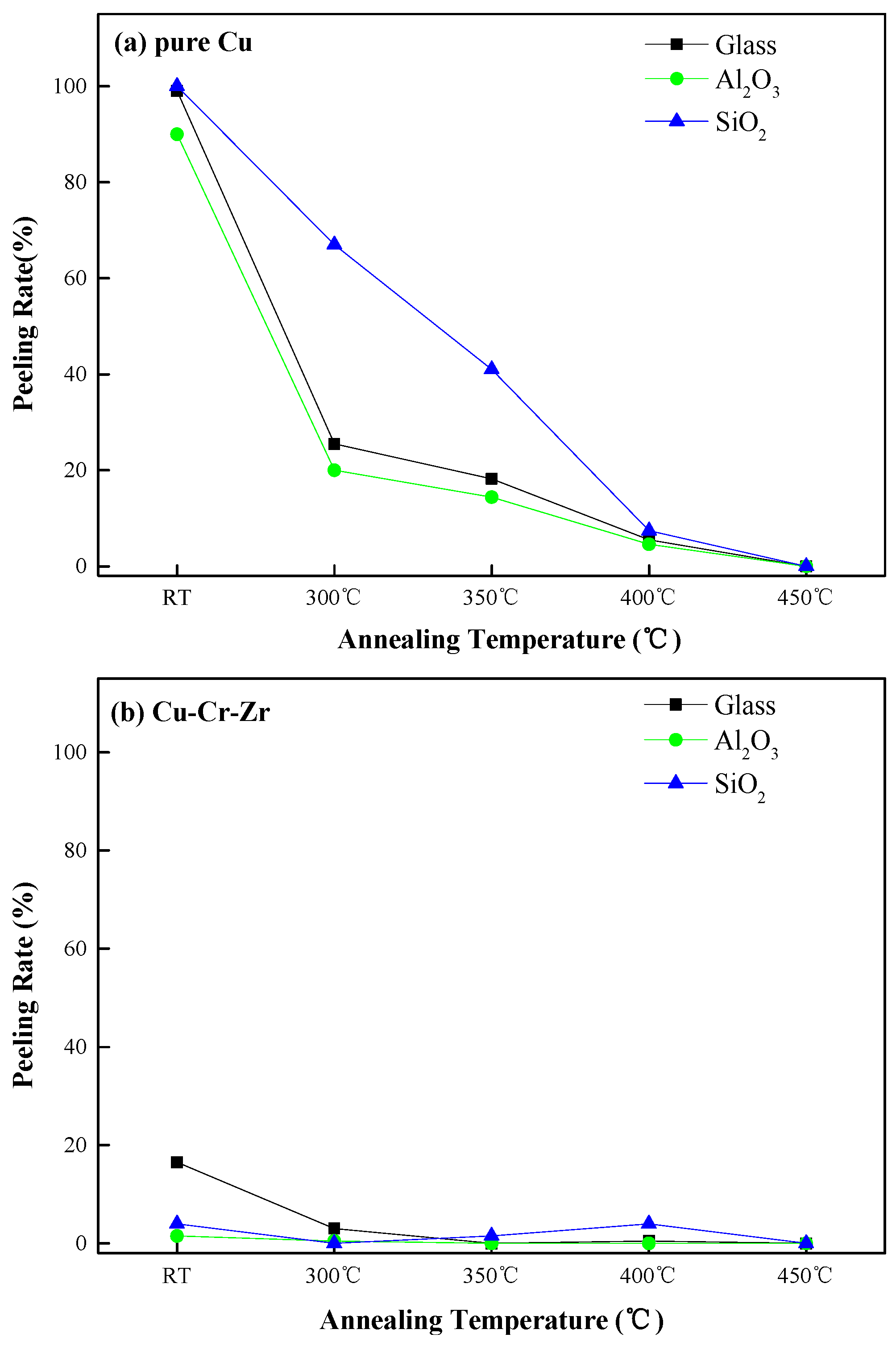
Figure 4.
XPS spectra of Cr2p core levels on the Cu-Cr-Zr thin film surface before and after annealing. The spectrum of annealed sample (circle dots) was fitted by the Shirley background (dashed line) and fitted with peaks of Cr2p3/2 (573.1 eV), Cr2p3/2 (573.9 eV), and Cr2p3/2 (575.1 eV) (dotted line).

Figure 5.
Focused Ion Beam (FIB)-TEM micrographs of the alloy thin films: (a) Cu-Cr-Zr film before annealing; (b) Cu-Cr-Zr film after annealing at 300 °C.
Figure 5.
Focused Ion Beam (FIB)-TEM micrographs of the alloy thin films: (a) Cu-Cr-Zr film before annealing; (b) Cu-Cr-Zr film after annealing at 300 °C.
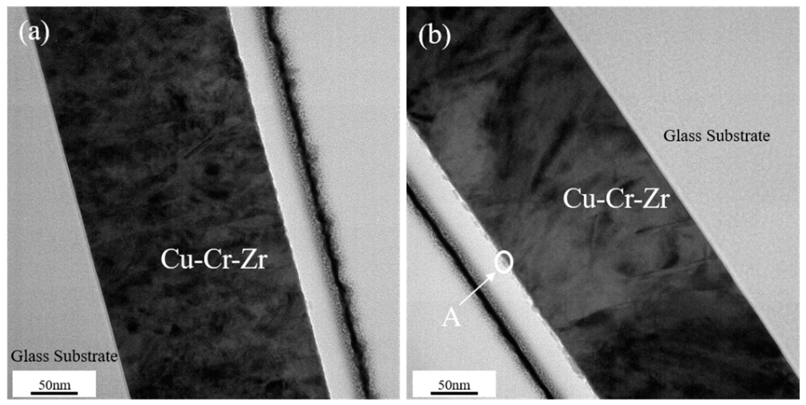
Figure 6.
The XRD of Cu-Cr-Zr and pure Cu thin-film samples.

Figure 7.
The XRD of Cu-Cr-Zr thin-film samples (a) at room temperature (RT), and after annealing at (b) 300 °C; (c) 350 °C; (d) 400 °C; and (e) 450 °C.
Figure 7.
The XRD of Cu-Cr-Zr thin-film samples (a) at room temperature (RT), and after annealing at (b) 300 °C; (c) 350 °C; (d) 400 °C; and (e) 450 °C.

Table 1.
Substrate parameters.
| Substrates | Sputtering Mode | Sputtering Power (W) | Ar Pressure (mTorr) | Thickness (Å) |
|---|---|---|---|---|
| Glass | ||||
| Al2O3/Glass | RF | 120 | 1 | 300 |
| SiO2/Glass | RF | 80 | 1 | 250 |
Table 2.
Classification of adhesion test results.
| Percent Area Removed | Classification |
|---|---|
| 0% | 5B |
| Less than 5% | 4B |
| 5–15% | 3B |
| 15–35% | 2B |
| 35–65% | 1B |
| Greater than 65% | 0B |
Table 3.
The grades of Cu-Cr-Zr thin film adhesion on various substrates.
| Substrates | Room Temperature (RT) | 300 °C | 350 °C | 400 °C | 450 °C |
|---|---|---|---|---|---|
| Glass | 2B | 4B | 5B | 4B | 5B |
| Al2O3/Glass | 4B | 4B | 5B | 5B | 5B |
| SiO2/Glass | 4B | 5B | 4B | 4B | 5B |
© 2017 by the authors. Licensee MDPI, Basel, Switzerland. This article is an open access article distributed under the terms and conditions of the Creative Commons Attribution (CC BY) license (http://creativecommons.org/licenses/by/4.0/).
Share and Cite
MDPI and ACS Style
Peng, J.; Lu, K.; Hu, S.; Fang, Z.; Ning, H.; Wei, J.; Zhu, Z.; Zhou, Y.; Wang, L.; Yao, R.; et al. High Conductivity and Adhesion of Cu-Cr-Zr Alloy for TFT Gate Electrode. Appl. Sci. 2017, 7, 820. https://doi.org/10.3390/app7080820
AMA Style
Peng J, Lu K, Hu S, Fang Z, Ning H, Wei J, Zhu Z, Zhou Y, Wang L, Yao R, et al. High Conductivity and Adhesion of Cu-Cr-Zr Alloy for TFT Gate Electrode. Applied Sciences. 2017; 7(8):820. https://doi.org/10.3390/app7080820
Chicago/Turabian StylePeng, Junbiao, Kuankuan Lu, Shiben Hu, Zhiqiang Fang, Honglong Ning, Jinglin Wei, Zhennan Zhu, Yicong Zhou, Lei Wang, Rihui Yao, and et al. 2017. "High Conductivity and Adhesion of Cu-Cr-Zr Alloy for TFT Gate Electrode" Applied Sciences 7, no. 8: 820. https://doi.org/10.3390/app7080820
Note that from the first issue of 2016, this journal uses article numbers instead of page numbers. See further details here.