A Power Processing Circuit for Indoor Wi-Fi Energy Harvesting for Ultra-Low Power Wireless Sensors

1
Faculty of Electrical Engineering, Universiti Teknologi Mara, Shah Alam 40450, Malaysia
2
Electrical and Computer Engineering Department, the University of Auckland, Auckland 1010, New Zealand
*
Authors to whom correspondence should be addressed.
Appl. Sci. 2017, 7(8), 827; https://doi.org/10.3390/app7080827
Submission received: 13 July 2017
/
Revised: 6 August 2017
/
Accepted: 7 August 2017
/
Published: 11 August 2017
(This article belongs to the Special Issue Smart Home and Energy Management Systems)
Abstract
:This article proposes a complete power processing circuit for an indoor 2.45 GHz Wi-Fi energy harvesting system. The proposed power processing circuit works by using power harvested from indoor Wi-Fi transmitters. The overall system of this work is simplified as an equivalent circuit and analyzed mathematically. A two-port network is analyzed in formulating the relevant equations of the equivalent circuit. The importance of matching the impedance of a harvesting antenna to the rectifier circuit is highlighted by using simulation analysis, and it is shown that the impedance matching for both components has satisfied the conditions for a high sensitivity circuit and radio frequency-to-direct current (RF-to-DC) power conversion. Actual experiments showed that the proposed power processing circuit could operate with an incident power as low as −50 dBm. It has been found that the proposed harvesting system stored 0.11 J in a 200 mF supercapacitor as the storage device in 20 hours of the experimentation periods. Moreover, actual results for the overall energy harvesting system is compared with previous research, and it has been found that the proposed system has advantages over the listed works.
1. Introduction
The latest development of low power consumption electronic device has contributed to a variety of energy smart wireless sensors. The wireless sensor collects data such as temperature, capacitance, vital signs, etc. Table 1 shows some low power wireless sensors and their typical power consumptions presented by Pcons. Mostly, the power requirements for the listed sensors are supplied by batteries. However, using batteries as an energy source has some disadvantages in the practical world, especially the replacement can be an issue when the stored energy is depleted. Alternatively, energy harvesting can be used as a new approach to powering wireless sensors. The energy harvesting system scavenges power from the ambient environment of wireless sensors, with popular ambient energy sources including thermal, vibrational, solar, electromagnetic, etc. And radio power transmitters can be used as an energy source for developling radio frequency energy harvesting systems (RFEHS), especially in urban areas where the transmitted radio frequency (RF) power is widely available at any time.
There is some drawback when RF sources such as Wi-Fi are used as an energy source for an RFEHS. The drawback is regarding power density, especially in an indoor area, where it is often very low [5]. Various RF power density levels for an outdoor environment in [6] have been summarized for several isotropic transmitters. In an indoor environment, a power density of 1 µW/cm2 at 2.45 GHz spectrum has been used to drive low-power low duty cycle applications [7]. Previous work on RFEHS has focused on single-band [8,9,10] and multi-band [11,12] operating frequencies. For multi-band frequencies energy harvesters, the amount of energy at the input can be high. However, due to the complexity of the multi-band system and the power drop at various rectifier diodes and power processing circuits, the radio frequency-to-direct current (RF-to-DC) conversion efficiency is often lower than the single-band RFEHS.
This research proposes a power processing circuit for a 2.45 GHz Wi-Fi indoor energy harvesting system which can accept the operational input power as low as −50 dBm. The proposed circuit acts also as an extension of a successful research reported in [13] with reduced charging time of the storage device. In this research, the analysis of the proposed power processing circuit with the other components of an RFEHS will be discussed using an equivalent circuit. A two-port network will be analyzed to derive the relevant equations for the equivalent circuit. Then simulation analysis on the impedance matching of the rectification circuit will show the effect of diode parameters on the operation of the proposed power processing circuit. At the end of this research, the power processing circuit will be tested in a practical environment to demonstrate its actual performance with all the components of the proposed RFEHS.
2. The Proposed Power Processing Circuit for the Radio Frequency Energy Harvesting System (RFEHS)
2.1. The General Block Diagram
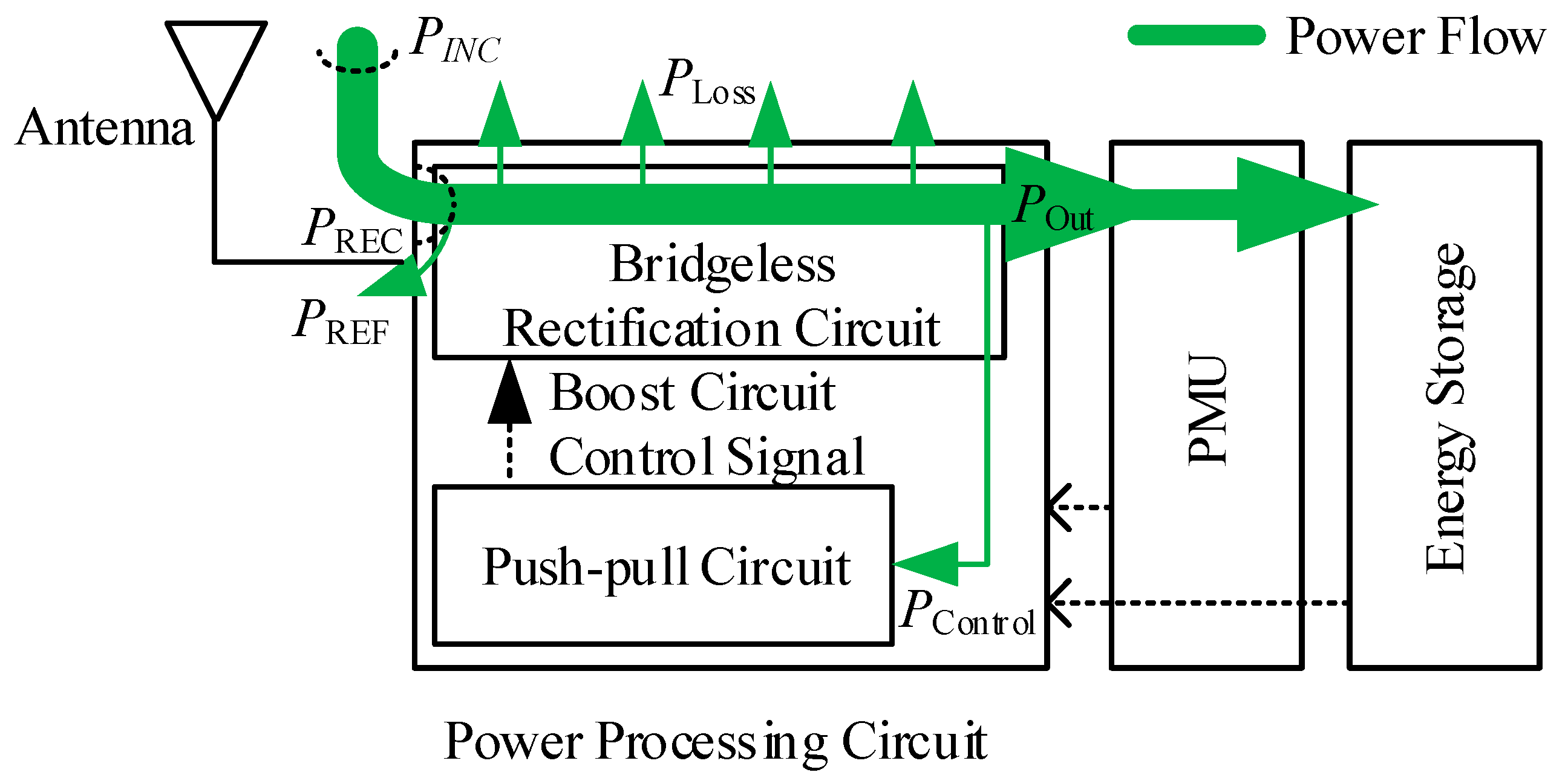
An illustration in Figure 1 shows a general block diagram of the proposed power processing circuit together with the power management unit (PMU) of the full RFEHS system. In the block diagram, PINC is the incident power at the energy harvester. PREC is the input power of the bridgeless rectification circuit, after the losses due to the energy harvester connector is subtracted from PINC. Typically, when integrating a radio frequency component with passive devices, an impedance mismatch between them will occur, and this contributes to some of the incident power is reflected. The reflected power is denoted as PREF. The power processing circuit consists of a bridgeless rectification circuit and a push-pull circuit. The function of the circuit is to process the received instantaneous power before the power is transferred to the PMU. The bridgeless rectification circuit and the push-pull circuit function are for generating a control signal for the boosting operation of the power processing circuit. The power needed to activate the push-pull circuitry is labelled as PControl. PLoss is the power lost during the proposed circuit operation which is from the microcontroller and circuit themselves. The output power of the power processing circuit is labelled as, POUT, where it uses the input power of the PMU. The PMU monitors and manages the output power of the circuit before storing it in an energy storage device.
2.2. The Schematic Circuit
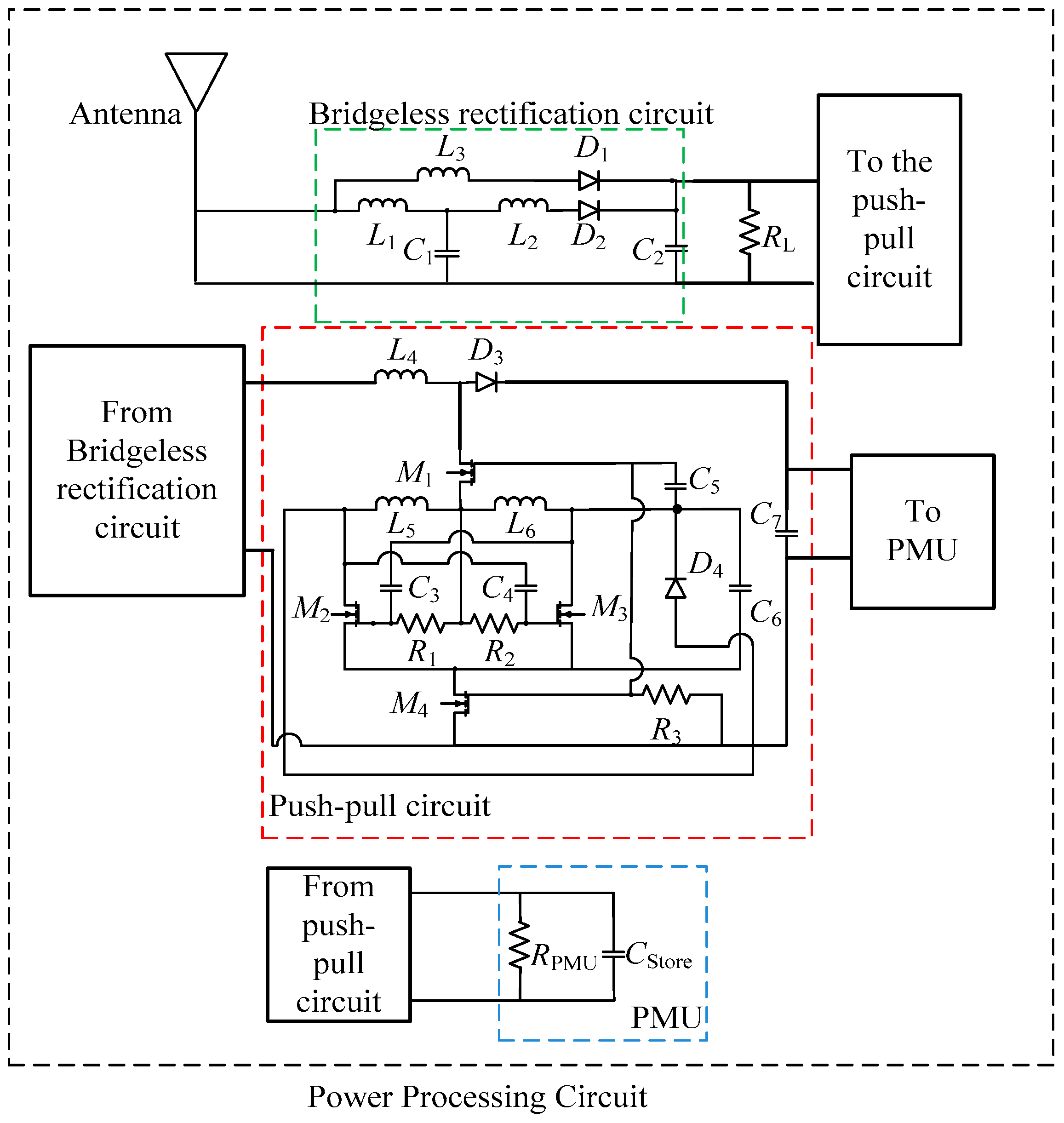
The schematic circuit of the general block diagram is depicted in Figure 2. For the bridgeless rectification circuit, L1, L2, and C1 are the parameters of a matching LCL network. L3 is an additional boost component that functions together with L1, L2, and C1. D1 and D2 are diodes for rectification and additional to the two branches. The output filter capacitor of the bridgeless rectifier is C2. The DC voltage level of C2 is the input voltage of the push-pull circuit. The inductor L4 is the inductor used for the power processing circuit-boosting operation. As illustrated in the figure the two switches M1 and M4 are used to control a shunt connection to the common terminal. Both switches are turned to ON and OFF synchronously, and the timing depends on the value of R3 and C5. Diode D4 is turned ON and OFF with regards to the alternating push-pull signal. The push-pull circuit is an arrangement of L5, L6, M2, M3, C3, C4, R1, and R2. Diode D3 maintains the direction of the current flow to the filter capacitor C6. The power management unit and the energy storage components of the proposed system are represented as RPMU and CSTORE.
3. Analytical Analysis
3.1. The Equivalent Circuit
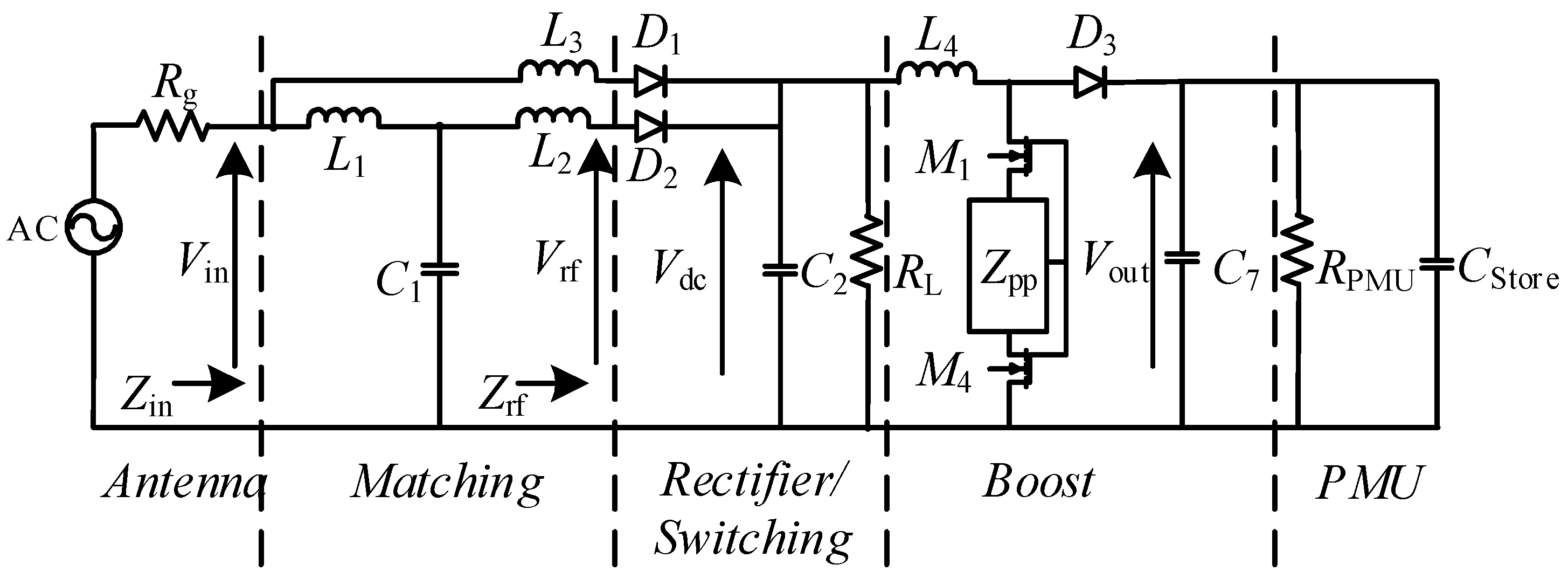
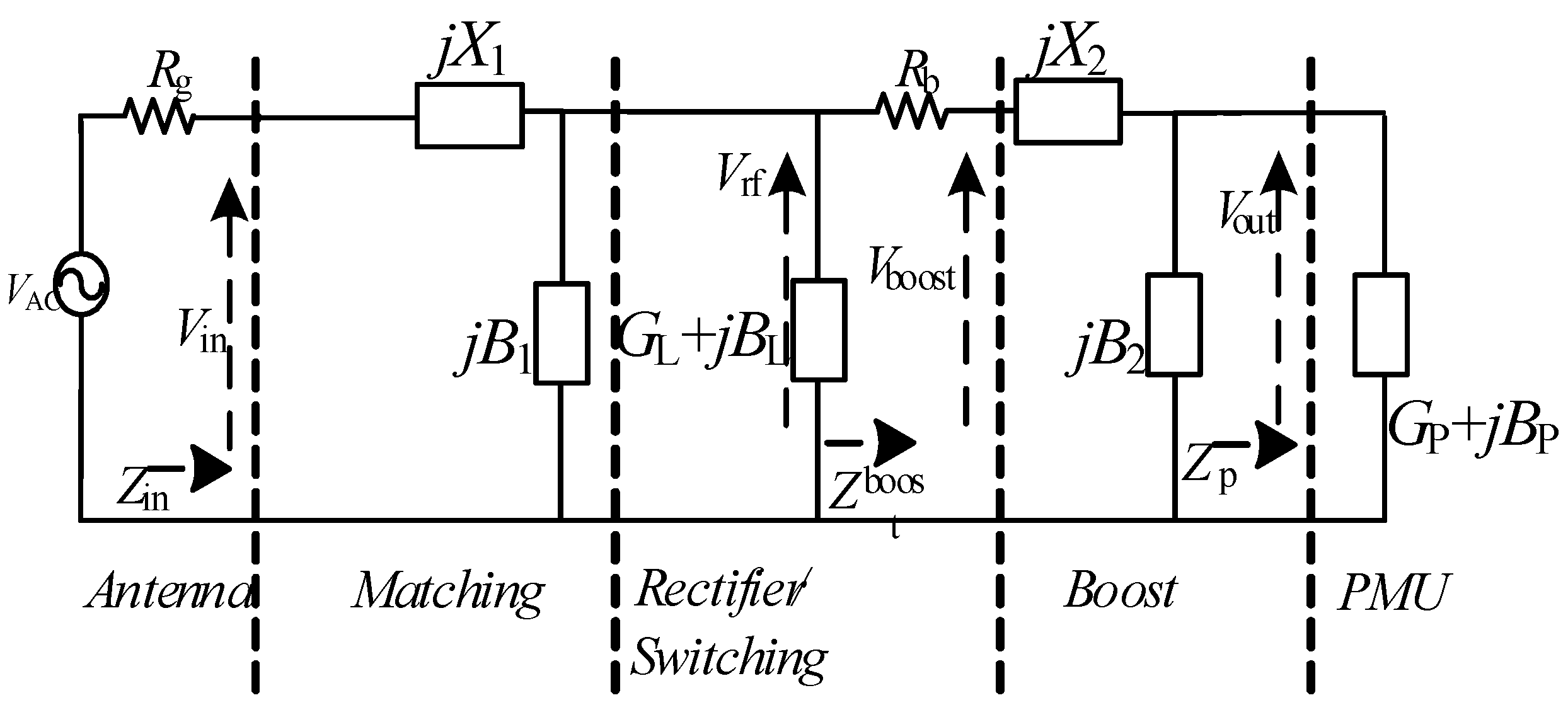
An equivalent circuit simplifying the schematic circuit is presented in Figure 3. Here, the receiving antenna is represented by an AC source with an internal resistance Rg. Vin is the input voltage of the matching circuit, Vrf is the input voltage of the rectifier/switching circuit, and Vdc is the direct current voltage across C2. Vout is the voltage measured at C7. Zin is the input impedance looking from the receiving antenna, and Zrf is the rectifier/switching input impedance. The impedance of the push-pull circuit is denoted as Zpp. The passive component in the equivalent circuit is transformed into complex impedances for simplifying the analysis as shown in Figure 4. At all input cycles, it is assumed that the diodes are acting as an ideal switch and the matching circuit is lossless.
The rectifier and the filter capacitor C2 are combined as a single load admittance YR = GL + jBL.
The input power of the circuit Pin can be calculated by
where Yin = 1/Zin and {𝑥} stands for the real part of complex variable Χ and Vin as shows in Figure 4. By applying Kirchhoff’s voltage and current laws, Vac − IRg = Vin = I/Yin, where I is the current flowing through Rg, then Equation (1) can be represented as
The output power of the rectenna or switching circuit is given by
where vrf is as indicated in Figure 4, and YL is the admittance as seen at the input of the rectifier/switching circuit.
3.2. Matched and Unmatched Antenna-Rectifier Circuit
The incident power dictates the output voltage of the matching circuit at the receiving antenna and the input impedance of the rectifying circuit. The two different matching conditions are considered; the conditions are when the antenna-rectifier is matched, and another condition is when the antenna-rectifier is unmatched. For the matched condition, the matching network as shown in Figure 4 is considered. To make sure the matching circuit conjugately matches the antenna to the rectifying circuit, the input impedance of the matching circuit needs to be equal to the antenna impedance (Zin = Rg) or YinRg = 1. Since the matching circuit is assumed lossless, the output power is assumed to be equal to the input power, Pout = Pin. The antenna-rectifying voltage gain can be written as
From Figure 4, the input impedance Zin for the antenna-rectifier matched condition can be calculated by
For the input impedance to be equal to Rg, the following two conditions must be applied which are:
The real part of the input admittance is given by
The circuit voltage gain for the antenna-rectifier matched condition is given by
where is the quality factor at the output of the matching circuit. As defined in (6), the rectifier/switching circuit defines parameter GL and BL. By proper choice of B1, the output voltage can be decided, and the value of Rg and X1 are calculated using (9). Indirectly, it is assumed that vac and Rg are chosen individually. Moreover, these two values are interrelated through the power available from the harvesting antenna, Pinc.
To calculate the output voltage at the end of the matching circuit, (6) and (9) are substituted into (10) to give the value of;
From (10), the voltage at the input of the rectifier/switching is consequently emitted by the available power from the harvesting antenna and the real part of the input admittance of the rectifier/switching circuit. Therefore, to maximise vrf, the real admittance of the rectifier/switching circuit needs to be as low as possible. For the condition when the impedance of the harvesting antenna and the rectifier circuit is unmatched, this gives and
where
The matching circuit output voltage, vrf, at this condition is written as
The output voltage of the matching circuit is identical to the output voltage for the matched situation multiplied by a multiplicative factor. This factor is equal to 1 for the case when the value of and (matched condition) is smaller than 1 for all situations. Hence, for the voltage to reach a maximum, the harvesting antenna should be impedance matched.
3.3. Rectifier Circuit Impedance Analysis
For the bridgeless rectification, Schottky diode is preferred as the component for the rectification operation. The diode has a very fast switching action and activates with a low forward bias voltage. The illustration in Figure 5 shows the diode in a series configuration with a source Vac and load. The source has an internal resistance Rg, and the load consists of a resistor RL in parallel with a capacitor CL.
The rectifier input impedance can be calculated by applying circuit analysis for the given diode model employing commercially available software. For the analysis, the value of the load capacitor, CL is assumed to be sufficiently large for the frequency range between 0.1 GHz to 2.5 GHz. Hence, the load is assumed to be in short circuit condition. Table 2 lists different diode parameters that could be uses for simulating the diode performance for some commercially available Schottky diodes. Parameter n is the emission coefficient of the diode. The type of Schottky diode used in the proposed circuit is SMS7621 from SKYWORKS (Woburn, MA, USA).
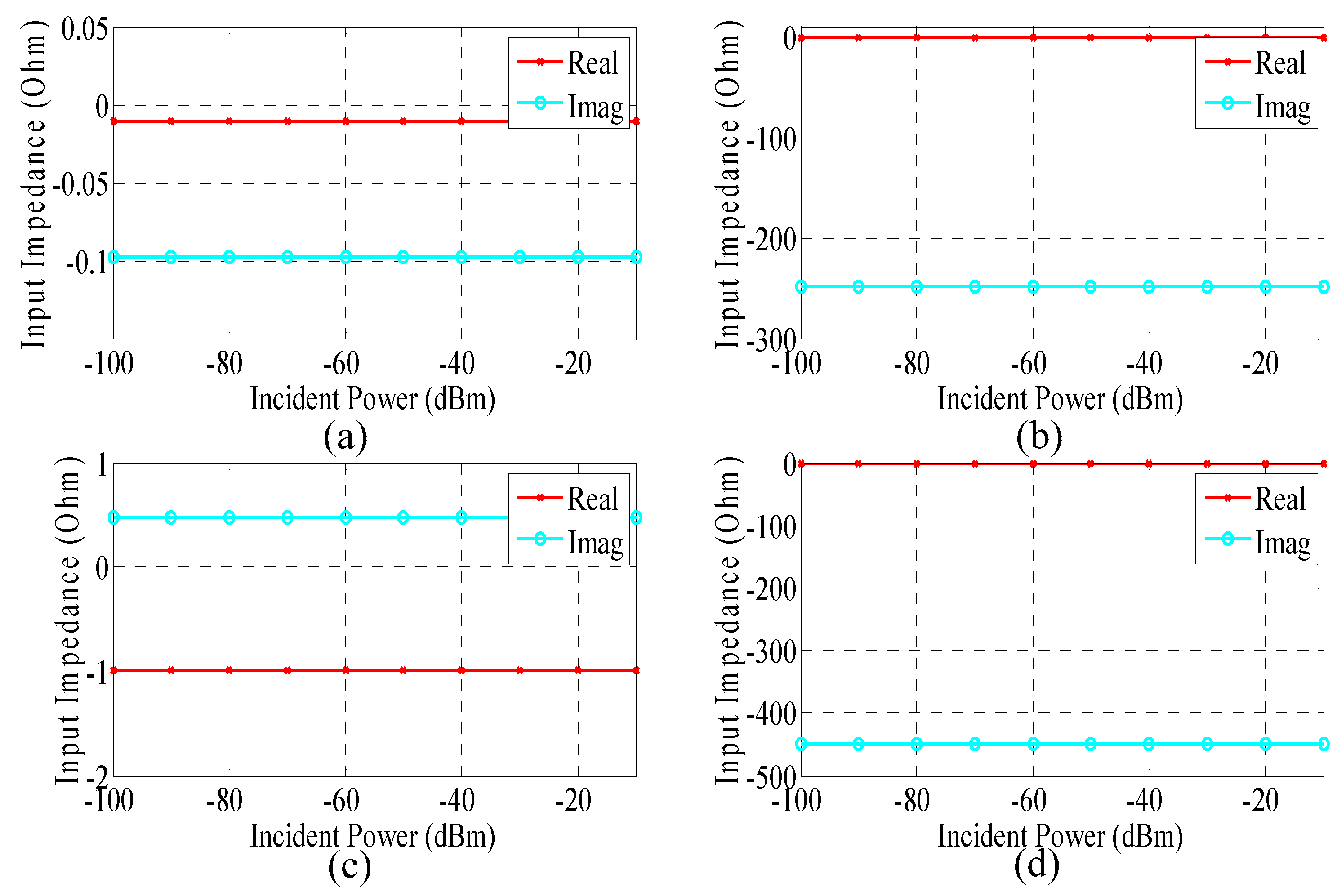
As labelled in Figure 4, the input voltage Vac follows from the relation between generator voltage and available incident power Pinc. The input impedance for a different commercially Schottky diode is depicted in Figure 6. In the figure, the simulation result of the real and imaginary parts of the input impedance as a function of available power Pinc for the frequency of 2.45 GHz is illustrated. The figure demonstrates that the input impedance satisfies the conditions for high sensitivity and RF-to-DC power conversion as required by Equation (11). From the simulation, it has been found that the real part of the input impedance for the selected Schottky diode is low, and the imaginary part absolute value for all types of diodes is high except for the HBAT5400. The highest imaginary part value shown in the figure is for the SMS7621 diode. The input impedance of the rectifier/switching circuit is also simulated with different frequencies, as seen in Figure 7 the impedance real value is at a constant value throughout the simulated frequencies at 6.4 Ohm. The imaginary value is gradually increasing as the frequencies move closer to 3 GHz. In short, the simulation results demonstrate that the rectifier/switching circuit satisfies the requirements for obtaining a high sensitivity circuit.
4. The Rectifying and Boost Circuit Characteristics
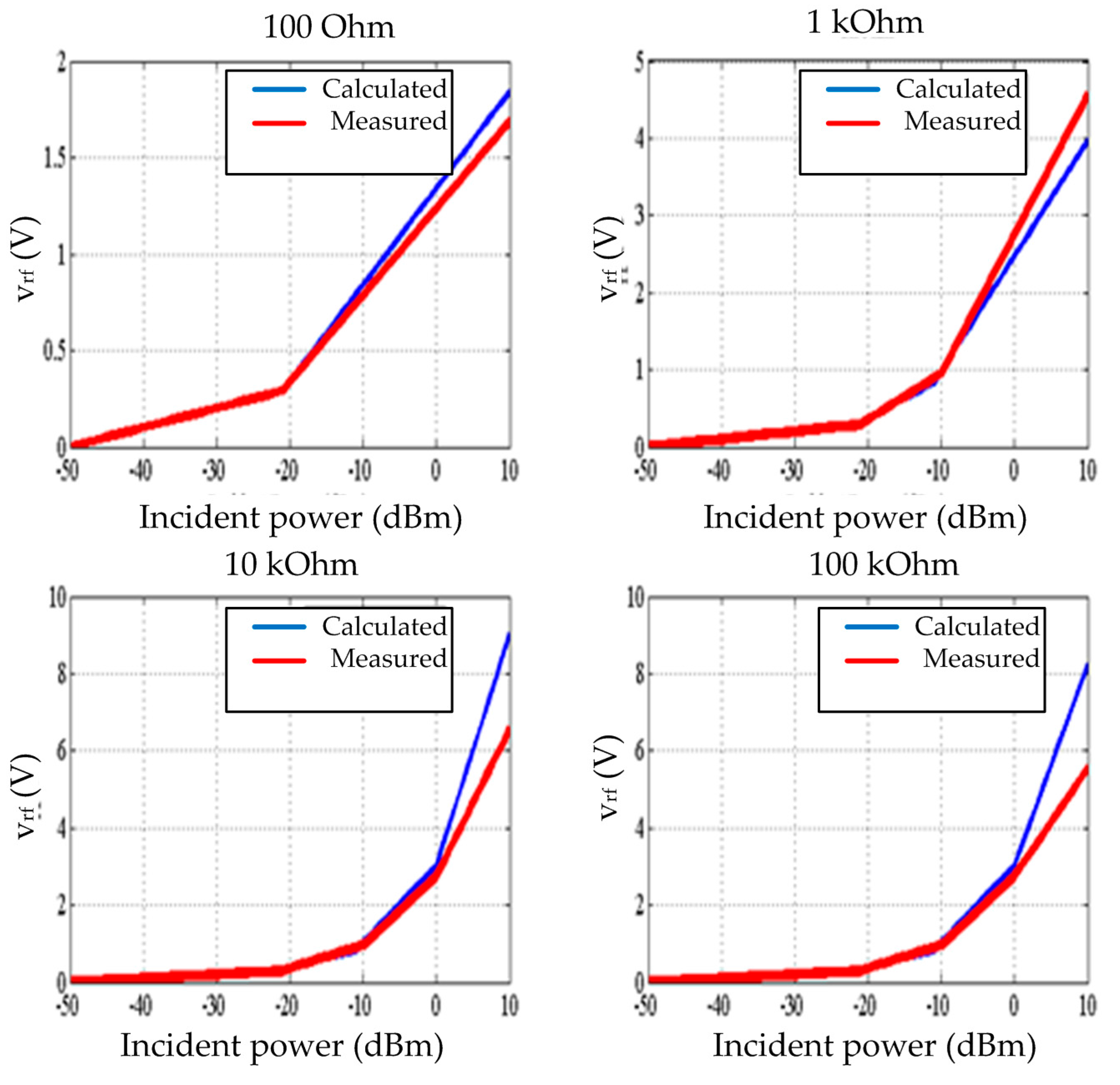
A mathematical approach such as Runge-Kutta (RK) has been used to analyse the DC behaviour of the circuit as in Figure 4, and the complete analysis is shown in [2]. A comparative analysis could have also been applied in analysing the diode behaviour [13]. In this work, the calculation of the DC output voltage after the rectifier circuit, vrf is done using Equation (10). The bridgeless rectification has been developed and the output voltage of the rectification circuit with the filter capacitor value of 10 µF is measured and reported in Figure 8.
A boost converter is accomplished in the proposed power processing circuit by switching a reactive component. Two n-channel MOSFET (NMOS) devices are used as the switches. Triggering the devices ON and OFF is done by a periodic signal generated by the push-pull circuit. When both switches are turned ON a current is flowing through the inductance L4. The output voltage vout is identical to vrf − vRb where vRb is the voltage drop due to the internal push-pull resistance. The diode is unbiased, and the output voltage vout is the voltage over the capacitor C7. When the switch is turned OFF, the voltage, vL4 is developed to keep the current flowing. The diode is now forward biased and the voltage vout = vrf − vRb + vL4 is transferred to the capacitor. As the switch is turned ON again, the diode is unbiased. A resistive load is draining the charge from C7. Upon opening the switch, C7 is recharged again.
5. Simulation Results of the Power Processing Circuit
There are three main points concerning the proposed power processing circuit that need to be investigated. These points highlight the voltage characteristics of the proposed power processing circuit. The three different points are the voltage across capacitor C2, the differential voltage at the positive terminal of diode D3 and the output voltage of the proposed circuit which is the voltage across C7. The signal characteristics of the three stated points can be found using circuit simulation. LT Spice software is utilised for investigation purposes. The spice parameters of the Schottky diode, SMS7621, and the NMOS switch, ALD210800A are obtained from the manufacturer datasheet.
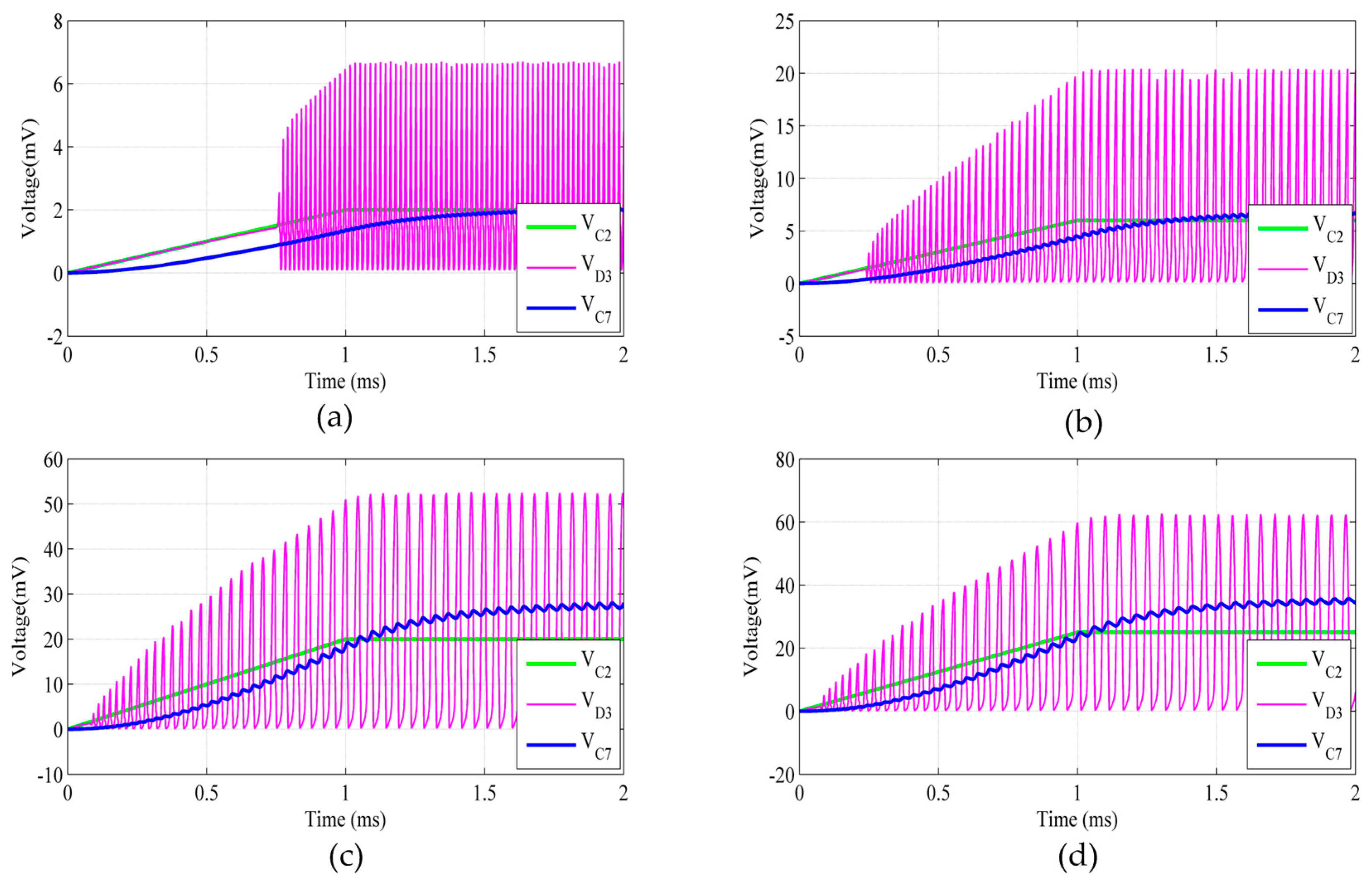
In the simulation, the harvesting antenna is assumed as an AC source. The AC source continuously supplies the power processing circuit with a sinusoidal input signal. The push-pull circuit operation is relating to the signals of the voltage across VC3 and VC4 which the driving signal for the switching MOSFET, M2 and M3. The inverting signal is measured at VC6. Figure 9 illustrates the signals for the stated components. As depicted in the figure, the instantaneous signal at VC6 is bigger than the VAC which is normally less than 10 mV. The higher the AC signal contributes to faster charging time for the storage component.
There are four different alternating input voltages were tested as the input signal for the proposed circuit and the values are 2 mVp-p, 6 mVp-p, 20 mVp-p and 35 mVp-p. For all the input voltages, the frequency is at 2.45 GHz. Each value represents an input power of −50 dBm, −40 dBm, −30 dBm and −25 dBm, respectively, being supplied to a 50 Ohm impedance input terminal. As illustrated in Figure 10, there is an initialization time for the power processing circuit to start the circuit boosting operation. The initialization time occurred because the stored energy in C2 is not enough to activate the boosting circuit. However, when the stored energy in C2 is sufficient, the boost circuit will start its function. In practical, it is expected that the initialization time will be longer since this incident signal is low and in burst mode. However, with respect to time, the energy level stored in C2 will reach the required level for boost circuit operational.
The boosting signal is represented by the simulation result of VD3. The circuit initialization time becomes shorter when the input voltage is bigger. As can be seen in Figure 10a,b, the time needed for the boost circuit to start functioning is approximately 0.8 ms, as the input voltage is increased to 6 mVp-p, and the time required for initialization less, which is approximately 0.25 ms. The initialization became much faster to approximately 0.1 ms when the input voltage is bigger than 20 mVp-p. The reading for VC2 and VC7 is not much difference especially for an input voltage of 2 mVp-p and 6 mVp-p. However, for higher input voltages, 20 mVp-p, and 35 mVp-p, there is a significant result obtained. The power processing circuit boosted the value of VC2 close to 3 times of the input voltage as shown in Figure 10c,d. From the simulation, it has been demonstrated that the boost circuit is functioning as expected. For a small input voltage 1 mVp (−50 dBm), the boost circuit of the proposed power processing circuit can generate 6 times bigger than the input voltage of the switching diode D3. The signal boost factor is close to 6.5 times. On average, for all the selected input voltages, the peak voltage signal measured at D3 is approximately 5.5 times greater than peak input voltage at C2. This condition shows that the power processing circuit can be used even when the input voltage value supplied is small.
6. The Proposed Power Processing Circuit Performance
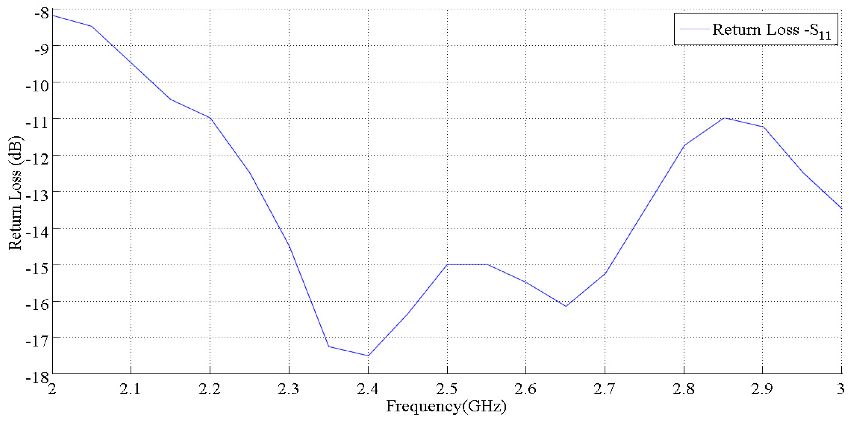
The matching circuit performance of the proposed power processing circuit is demonstrated by measuring the return loss at the input terminal of the circuit. A vector network analyser measured the return loss, and the result is depicted in Figure 11. As reported in the figure, the lowest return loss is approximate at −17.5 dB, which is at 2.4 GHz. At 2.45 GHz, the return loss is at −16.5 db.
The proposed power processing circuit is fabricated, and the component values of the proposed power processing circuit are listed in Table 3.
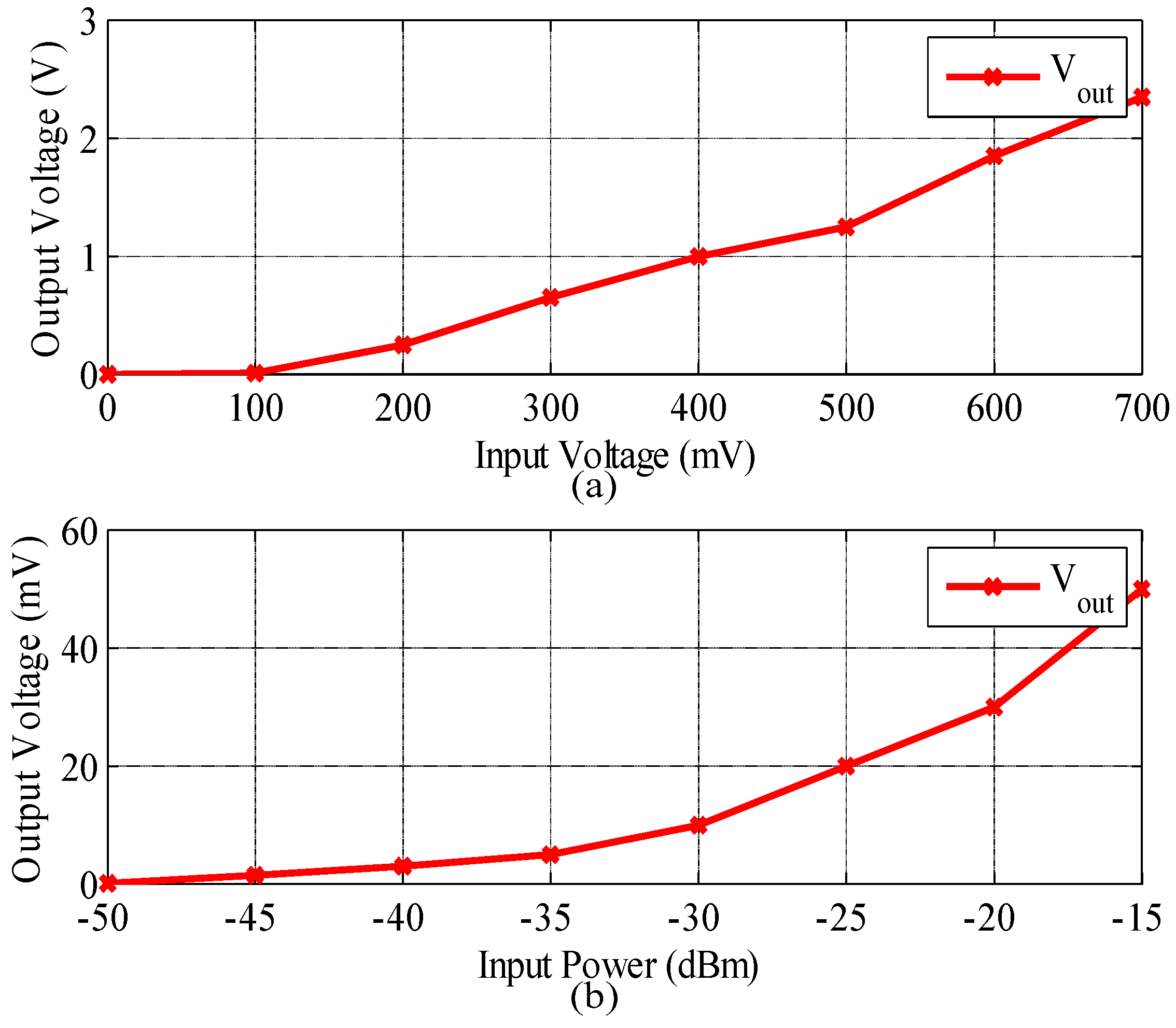
The developed power processing circuit is tested with a varying input voltage and power which is injected by an RF signal generator. This step is taken to demonstrate that the proposed power processing circuit can rectify instantaneous input signal, accordingly. For this experiment, a load resistor and a capacitor are connected to the output terminal of the circuit, and the value is 10 kΩ and 0.1 µF, respectively. The reading obtained from the experiment is reported in Figure 12, it is found that the circuit output voltage level reached 1.8 V and 35 mV, for an input of 620 mVp and −20 dBm, respectively.
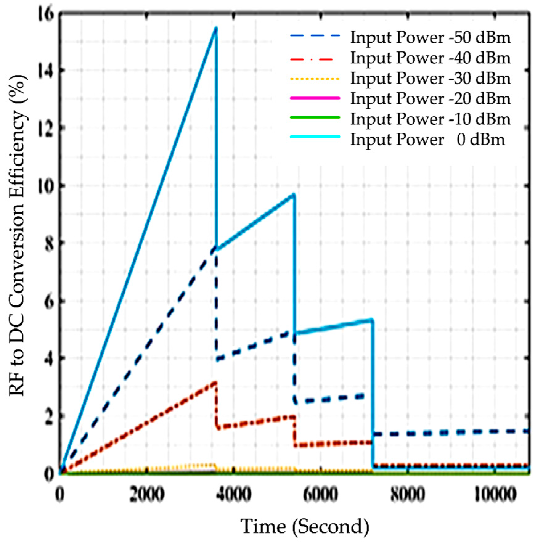
The capacitance of CSTORE is changed to 0.22 F to investigate the time required for the voltage across the capacitor to reach a constant level. The capacitance value is the lowest supercapacitor commercially available in the market. The supercapacitor is from Copper-Bussmann, and the equivalent series resistance (ESR) of the capacitor is less than 2 Ω. A signal generator supplies five different input powers at 2.45 GHz, and the voltage across CSTORE is recorded using the data logger. The measurement results are illustrated in Figure 13. From the measured value, it was noticed that the charging time could be divided into four separate phases as highlighted in Figure 13a. The period for each step is approximately ø1 = 0 s < t < 3600 s, ø2 = 3600 s < t < 5400 s, ø3 = 5400 s < t < 7200 s and ø4 = 7200 s < t < 10800 s. The voltage across CSTORE increased linearly during ø1 and steadily increased for ø2 and ø3. For the period of ø4 the voltage across the capacitor is constant. The current flow through the capacitor can be calculated by differentiating the measured voltage with respect to time , then multiplying by the capacitance of CSTORE, and the result is shown in Figure 13b. The current flow through the capacitor is the highest during ø1 for all levels of input power, and at the lowest towards ø4 as the capacitor starts to behave in a saturation condition. By multiplying the voltage and current, the amount of power absorbed by CSTORE is depicted in Figure 13c. The energy stored in the capacitor is estimated by using , and the value is reported in Figure 13d. The RF-to-DC conversion efficiency for the proposed system can be plotted as a function of DC output power over the radio frequency input power, and the result is illustrated in Figure 14. From the figure, it is noticed that the proposed system gives an efficiency of more than 1% for an input power of −50 dBm, −40 dBm, −30 dBm and 0 dBm. However, for an input power of −20 dBm and −10 dBm the efficiency is less than 1%. The RF-to-DC conversion efficiency values show that the proposed system is suitable for working with low and medium input power. This condition is not much different with another type of harvesting systems which are normally optimised to work with low input power.
7. Actual Experimentation of the RFEHS
In this section, the performance of the proposed power processing circuit experimented in a real environment is highlighted. In the experiment, the input terminal of the proposed power processing circuit is connected to a 50-Ohm antenna, where the antenna is designed to operate at 2.45 GHz. The energy harvester is a printed co-planar waveguide antenna. The antenna is attached to the input of the circuit through a Sub-Miniature Version A (SMA) connector. The SMA connector impedance is 50 Ohm. The actual figure of the energy harvester is depicted in Figure 15. The detailed explanation of the antenna and its performance has been reported in [14].
The impedance losses when the power processing circuit is attached to the harvesting antenna is another system characteristic which needs to be highlighted. The effect on impedance losses can be seen by measuring the return loss with and without the power processing circuit attached to the antenna. Figure 16 illustrates the measured return loss, S11 for both conditions. As can be seen from the figure, the impedance losses are small, and the value is above the equator of the Smith chart, reflecting the harvesting antenna and the proposed power processing circuit inductive characteristics.
A PMU is attached to the output terminal of the proposed power processing circuit as shown in Figure 17. On the PMU, a supercapacitor is connected to the energy storage component. The arrangement of the harvesting antenna, the proposed power processing circuit and a PMU, made a complete RF energy harvesting system. During the measurement period, the radio frequency signal strength inside the selected indoor area is monitored using Wi-Fi analyser software that is installed in a notebook and using a spectrum analyser connected to a similar antenna of the energy harvester for the proposed system. It has been found that the signal strength measured using both measurement devices are in good agreement. The measured signal strength result is illustrated in Figure 18. It has been found that during the test period, the transmitted signal is low. However, even the incident power is low, there are multiple numbers of incident power received at the energy harvester, continuously, and the amount is sufficient for the operation of the proposed harvesting system. During the measurement periods, it has been found that four 2.4 GHz Wi-Fi access points are covering the selected area.
As can be seen in Figure 18, the maximum peak of the signal strength is −55 dBm, and the lowest is between −85 dBm. The available power that could be transferred from the antenna to the matching circuit can be calculated by a function of PINC = Pmeasured + 30 dBm. For an example, let us assume the transmitted power (PTx) for Wi-Fi transmitter is 0 dBm, and the average power received at the antenna is approximate −60 dBm. The losses introduced during the power transmission can be calculated by substituting the transmitted power with the average received power which gives the estimated losses to be 0 dBm-(−60 dBm) = 60 dBm. Then, the loss introduced by antennae and connector can be calculated which is 60 dBm/2 = 30 dBm. Hence, PINC for the level of the signal is −30 dBm. In practical, as shown in Figure 18, if the lowest measured signal strength is −85 dBm, the available power that is transferred to the matching circuit is at −55 dBm.
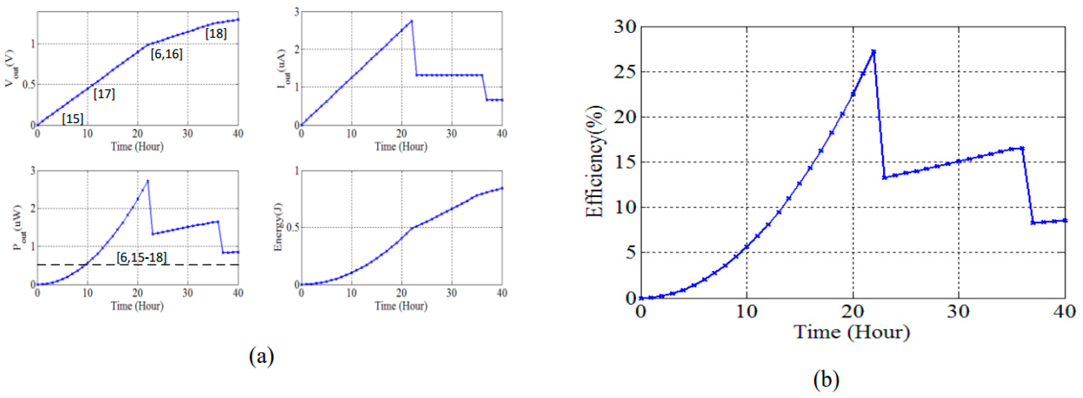
The voltage across the 0.22 F super capacitor connected to the output of the PMU is measured. The value is recorded using a data logging instrument from National Instrument known as ELVIS II. For the actual experimentation, the targeted voltage across CSTORE is 1 V. The time taken for the voltage to reach that level is approximately 20 h. The harvesting time approximation can be calculated by:
where T is the time in an hour, and ic is approximately close to 3 µA which also has been discussed in [14]. From the recorded results, the current through the capacitor, the power absorbed and the energy stored in the capacitor are calculated and reported in Figure 19. Comparison with others finding as listed in Table 4 is labeled in the figure.
The proposed system needs less than five hours to gain the minimum power requirements for all the listed sensors. The RF to DC conversion efficiency of the system is calculated by dividing the output power, Pstore, of the storage capacitor by the available input power of the matching circuit, PRF. However, since the value of Pstore increases over time as calculated, the efficiency of the system is calculated in term of ranges. If the highest signal strength recorded (≈−50 dBm) is assumed to be the dominant incident power to the proposed system over time, that gives the available power to the circuit being close to PINC = (−55 + 30) dBm = −20 dBm or 10 µW. The efficiency of the system is calculated and illustrated in Figure 19b. As shown in the figure, the efficiency of the overall system increased over time and the highest efficiency achieved is close to 30%. The efficiency dropped close to 6% as the voltage across the storage capacitor reached a constant level. As illustrated in Figure 14, the efficiency of the proposed system before the PMU is connected at the end of boost circuit is less than 1% for −20 dBm input power. However, with the addition of the PMU, the efficiency is improved with respect to time. Finally, from all the measurement values, the key features of the proposed RFEHS are listed Table 5.
8. Harvesting System Performance Comparison
The performance of the proposed harvesting system with another previous work is summarized in Table 6. The comparison is made with others RF energy harvesting systems which used input powers approximately −50 dBm to 0 dBm. By comparing the RF-to-DC efficiency of the proposed harvesting system to the stated previous research, work in [19] has the highest efficiency. However, the result was obtained using −10 dBm input power. From the comparison table, it is clearly shown that the proposed RFEHS performs better than the dual or multiband frequencies RF energy harvesting system. The proposed RFEHS also produced a similar performance with other listed research. Moreover, the circuit has operated by using power harvested from non-dedicated RF sources.
9. Conclusions
This paper presents a method for designing a complete power processing circuit for an indoor RF energy harvesting system. The analytical analysis of the power processing circuit attached to an antenna and a PMU has been conducted based on an equivalent circuit. The impedance matching between the energy harvester, matching circuit and rectifier circuit have been analysed. From the simulation analysis, it has been demonstrated that the selected Schottky diode used in designing the proposed power processing circuit gave the best performance compared to other diodes. The power processing circuit works well with Wi-Fi power typically at −20 dBm, which can even go down to as low as −50 dBm. The overall RF-to-DC power efficiency of 30% is obtained from the proposed energy harvesting system. The final measurement result has demonstrated that the proposed system can charge up a 200 mF supercapacitor in 20 hours, and the stored energy of 0.11 J can be used to drive low power wireless sensors.
Acknowledgments
The main funding for the research works is from the Postgraduate Research Student Support (PReSS account), The University of Auckland, New Zealand.
Author Contributions
Ermeey Abd Kadir conceived and designed the experiments; Ermeey Abd Kadir performed the experiments; Ermeey Abd Kadir analyzed the data; Ermeey Abd Kadir contributed analysis tools; Ermeey Abd Kadir wrote the paper; Aiguo Patrick Hu proposed the research topic and supervised the research progress.
Conflicts of Interest
The authors declare no conflict of interest.
References
- Shenghua, Z.; Nanjian, W. A novel ultra low power temperature sensor for UHF RFID tag chip. In Proceedings of the ASSCC’07. IEEE Asian Solid-State Circuits Conference, Jeju, Korea, 12–14 November 2007; pp. 464–467. [Google Scholar]
- Visser, H.J.; Vullers, R.J. Wireless sensors remotely powered by RF energy. In Proceedings of the 2012 6th European Conference on Antennas and Propagation (EUCAP), Prague, Czech Republic, 26–30 March 2012; pp. 1–4. [Google Scholar]
- Zou, X.; Xu, X.; Yao, L.; Lian, Y. A 1-V 450-nW fully integrated programmable biomedical sensor interface chip. IEEE J. Solid State Circuits 2009, 44, 1067–1077. [Google Scholar] [CrossRef]
- Urard, P.; Romagnello, G.; Banciu, A.; Grasset, J.C.; Heinrich, V.; Boulemnakher, M.; Todeschni, F.; Damon, L.; Guizzetti, R.; Andre, L.; et al. A self-powered IPv6 bidirectional wireless sensor & actuator network for indoor conditions. In Proceedings of the 2015 Symposium on VLSI Circuits (VLSI Circuits), Kyoto, Japan, 17–19 June 2015; pp. 100–101. [Google Scholar]
- Mimis, K.; Gibbins, D.; Dumanli, S.; Watkins, G.T. Ambient RF energy harvesting trial in domestic settings. IET Microw. Antennas Propag. 2014, 9, 454–462. [Google Scholar] [CrossRef]
- Lu, X.; Wang, P.; Niyato, D.; Hossain, E. Dynamic spectrum access in cognitive radio networks with RF energy harvesting. IEEE Wirel. Commun. 2014, 21, 102–110. [Google Scholar] [CrossRef]
- Liao, Y.; Zhang, Y.; Cai, K.; Gao, W. A Simple Equivalent Circuit for Small RFID Tag Antennas in Low Loss Dielectric Materials. In Applied Mechanics and Materials; Trans Tech Publication: Stafa-Zurich, Switzerland, 2013; pp. 1470–1473. [Google Scholar]
- Sum, Y.L.; Soong, B.H.; Tseng, K.J. Selection of unit cell size for RF energy harvesting metaresonator array. In Proceedings of the 5th IET International Conference on Renewable Power Generation (RPG), London, UK, 21–23 September 2016. [Google Scholar]
- Choi, M.; Jang, T.; Jeong, J.; Jeong, S.; Blaauw, D.; Sylvester, D. A Resonant Current-Mode Wireless Power Receiver and Battery Charger With -32 dBm Sensitivity for Implantable Systems. IEEE J. Solid State Circuits 2016, 51, 2880–2892. [Google Scholar] [CrossRef]
- Masuch, J.; Delgado-Restituto, M.; Milosevic, D.; Baltus, P. Co-integration of an RF energy harvester into a 2.4 GHz transceiver. IEEE J Solid State Circuits 2013, 48, 1565–1574. [Google Scholar] [CrossRef]
- Mrnka, M.; Vasina, P.; Kufa, M.; Hebelka, V.; Raida, Z. The RF Energy Harvesting Antennas Operating in Commercially Deployed Frequency Bands: A Comparative Study. Int. J. Antennas Propag. 2016. [Google Scholar] [CrossRef]
- Sample, A.P.; Parks, A.N.; Southwood, S.; Smith, J.R. Wireless ambient radio power. In Wirelessly Powered Sensor Networks and Computational RFID; Springer: Berlin, Germany, 2013; pp. 223–234. [Google Scholar]
- Shashkin, V.I.; Murel, A.V. Comparative analysis of microwave low-barrier Mott and Schottky detector diodes. In Proceedings of the 20th International Crimean Conference on Microwave and Telecommunication Technology (CriMiCo), Sevastopol, Ukraine, 13–17 September 2010; pp. 829–830. [Google Scholar]
- Kadir, E.A.; Hu, A.P.; Biglari-Abhari, M.; Aw, K.C. A bridgeless rectification circuit for Wi-Fi energy harvesting system. In Proceedings of the IEEE Energy Conversion Congress and Exposition (ECCE), Montreal, QC, Canada, 20–24 September 2015; pp. 421–426. [Google Scholar]
- Bandyopadhyay, S.; Mercier, P.P.; Lysaght, A.C.; Stankovic, K.M.; Chandrakasan, A.P. A 1.1 nW energy-harvesting system with 544 pW quiescent power for next-generation implants. IEEE J. Solid State Circuits 2014, 49, 2812–2824. [Google Scholar] [CrossRef] [PubMed]
- Reinisch, H.; Gruber, S.; Unterassinger, H.; Wiessflecker, M.; Hofer, G.; Pribyl, W.; Holweg, G. An electromagnetic energy harvesting system with 190 nW idle mode power consumption for a BAW based wireless sensor node. IEEE J. Solid State Circuits 2011, 46, 1728–1741. [Google Scholar] [CrossRef]
- Saw, S.K.; Nath, V. A 10.8 nW low power CMOS temperature sensor for a wireless application. In Proceedings of the International Conference on Electrical, Electronics, Signals, Communication and Optimization (EESCO), Visakhapatnam, India, 24 January 2015; pp. 1–3. [Google Scholar]
- Jeong, S.; Foo, Z.; Lee, Y.; Sim, J.Y.; Blaauw, D.; Sylvester, D. A fully-integrated 71 nW CMOS temperature sensor for low power wireless sensor nodes. IEEE J. Solid State Circuits 2014, 49, 1682–1693. [Google Scholar] [CrossRef]
- Kuhn, V.; Lahuec, C.; Seguin, F.; Person, C. A multi-band stacked RF energy harvester with RF-to-DC efficiency up to 84%. IEEE Trans. Microw. Theory Tech. 2015, 63, 1768–1778. [Google Scholar] [CrossRef]
- Collado, A.; Georgiadis, A. Conformal hybrid solar and electromagnetic (EM) energy harvesting rectenna. IEEE Trans. Circuits Syst. I Regul. Pap. 2013, 60, 2225–2234. [Google Scholar] [CrossRef]
- Georgiadis, A.; Andia, G.V.; Collado, A. Rectenna design and optimization using reciprocity theory and harmonic balance analysis for electromagnetic (EM) energy harvesting. IEEE Antennas Wirel. Propag. Lett. 2010, 9, 444–446. [Google Scholar] [CrossRef]
- Li, B.; Shao, X.; Shahshahan, N.; Goldsman, N.; Salter, T.; Metze, G.M. An antenna co-design dual band RF energy harvester. IEEE Trans. Circuits Syst. I Regul. Pap. 2013, 60, 3256–3266. [Google Scholar] [CrossRef]
- Parks, A.N.; Smith, J.R. Active power summation for efficient multiband RF energy harvesting. In Proceedings of the IEEE MTT-S International conference on Microwave Symposium (IMS), Phoenix, AZ, USA, 17–22 May 2015; pp. 1–4. [Google Scholar]
Figure 1.
The general block diagram of the proposed system.

Figure 2.
The schematic circuit of the proposed system.

Figure 3.
The equivalent circuit.

Figure 4.
The simplified circuit.

Figure 5.
A series configuration with a source and load of a diode circuit model.
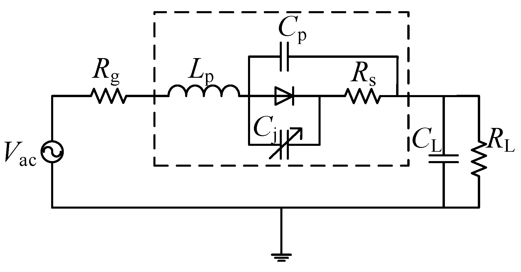
Figure 6.
Radio frequency (RF) input impedance versus Pinc at f = 2.45 GHz for some commercially Schottky diodes.
Figure 6.
Radio frequency (RF) input impedance versus Pinc at f = 2.45 GHz for some commercially Schottky diodes.

Figure 7.
The input impedance of the rectifier/switching circuit versus frequencies.
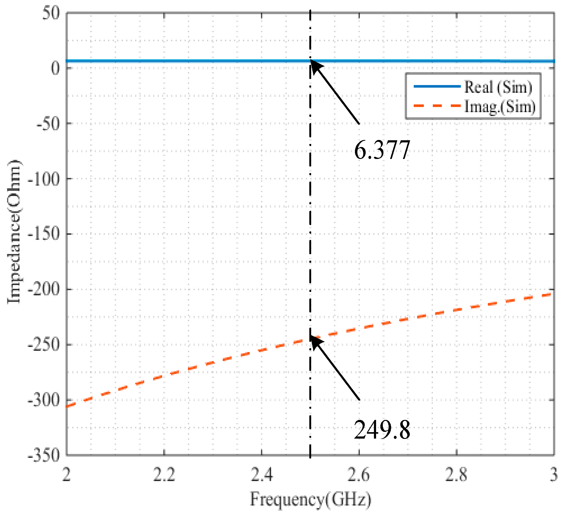
Figure 8.
The calculated and measured voltage of the rectification circuit as a function of available power for SMS7621 Schottky diodes at f = 2.45 GHz. Rg = 50 Ω.
Figure 8.
The calculated and measured voltage of the rectification circuit as a function of available power for SMS7621 Schottky diodes at f = 2.45 GHz. Rg = 50 Ω.

Figure 9.
The signals at VC3, VC4 and VC6 for an input signal of Vac = 3 mV and frequency of 2.45 GHz.
Figure 9.
The signals at VC3, VC4 and VC6 for an input signal of Vac = 3 mV and frequency of 2.45 GHz.
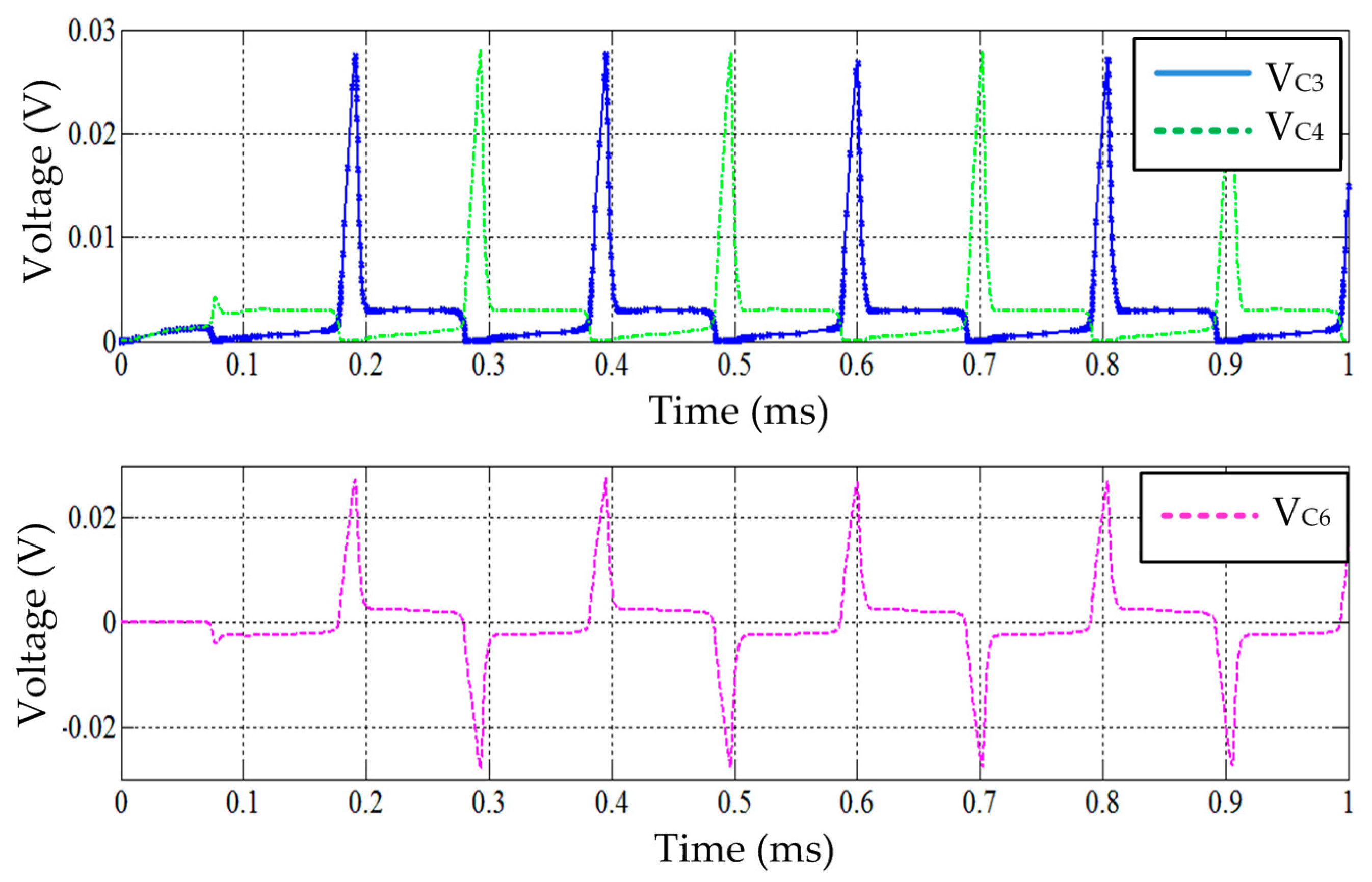
Figure 10.
The simulation result at the three most important testing points for the proposed power processing circuit when VAC is (a) 2 mVp-p, (b) 6 mVp-p, (c) 20 mVp-p and (d) 35 mVp-p.
Figure 10.
The simulation result at the three most important testing points for the proposed power processing circuit when VAC is (a) 2 mVp-p, (b) 6 mVp-p, (c) 20 mVp-p and (d) 35 mVp-p.

Figure 11.
The actual matching circuit return loss (S11).

Figure 12.
The measured output voltage versus peak input voltage (a), and input power (b) when RPMU =10 kΩ and CSTORE = 0.1 µF.
Figure 12.
The measured output voltage versus peak input voltage (a), and input power (b) when RPMU =10 kΩ and CSTORE = 0.1 µF.

Figure 13.
The measurement results of (a) Voltage across CSTORE; (b) Current through CSTORE; (c) Output power and (d) Stored energy.
Figure 13.
The measurement results of (a) Voltage across CSTORE; (b) Current through CSTORE; (c) Output power and (d) Stored energy.
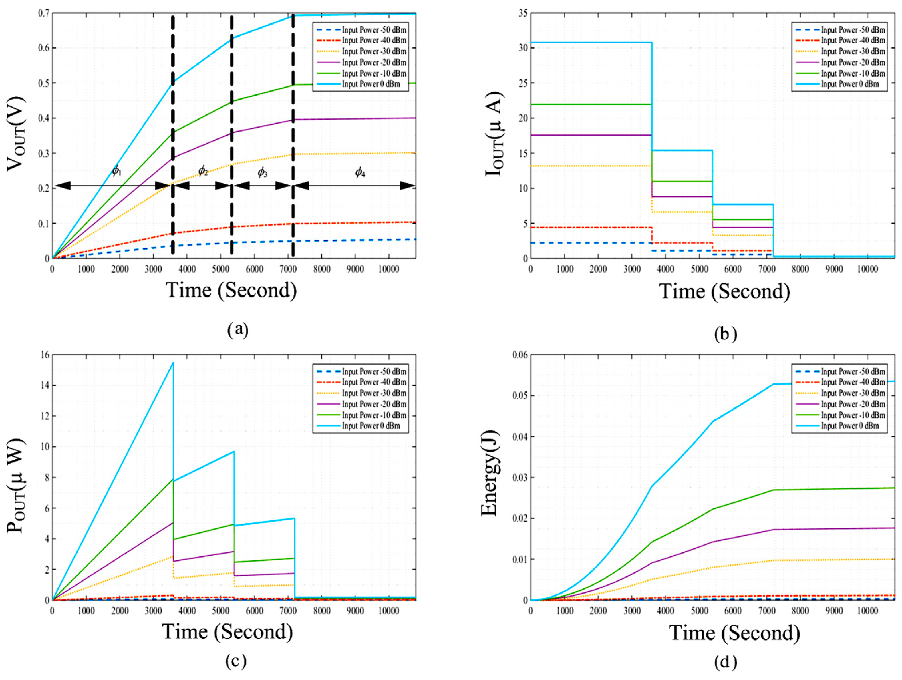
Figure 14.
The harvesting antenna and proposed power processing circuit RF-to-DC conversion efficiency versus time.
Figure 14.
The harvesting antenna and proposed power processing circuit RF-to-DC conversion efficiency versus time.

Figure 15.
A 50 Ω, 2.45 GHz coplanar waveguide antenna.
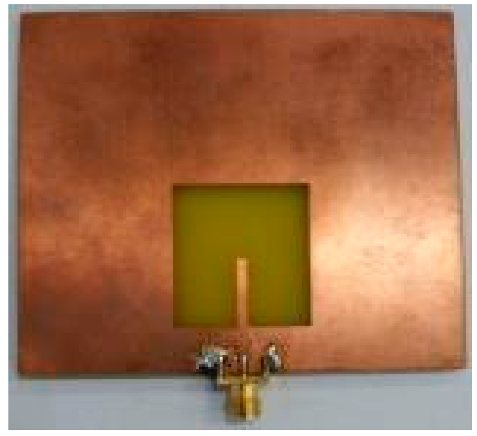
Figure 16.
Measured impedance losses of the harvesting antenna without and after attachment of the power processing circuit at 2.45 GHz.
Figure 16.
Measured impedance losses of the harvesting antenna without and after attachment of the power processing circuit at 2.45 GHz.
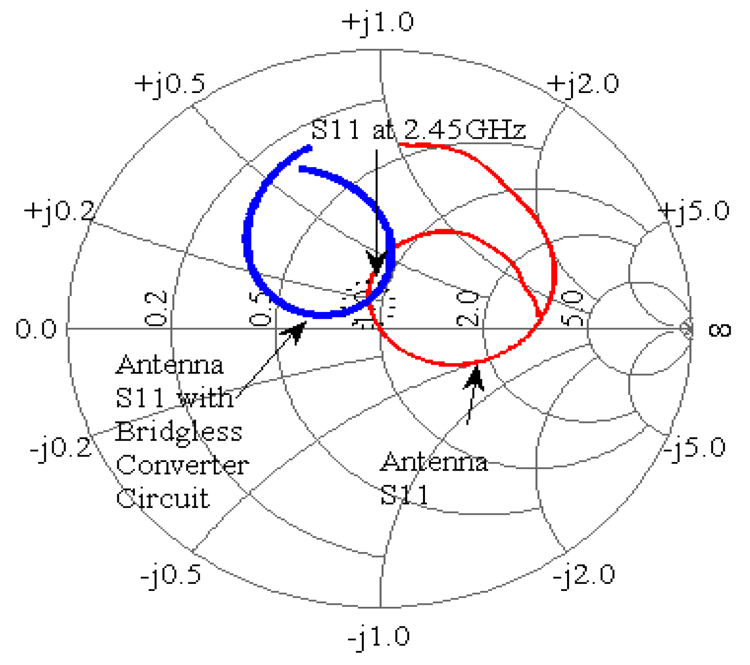
Figure 17.
The actual figure of the proposed RF energy harvesting system.
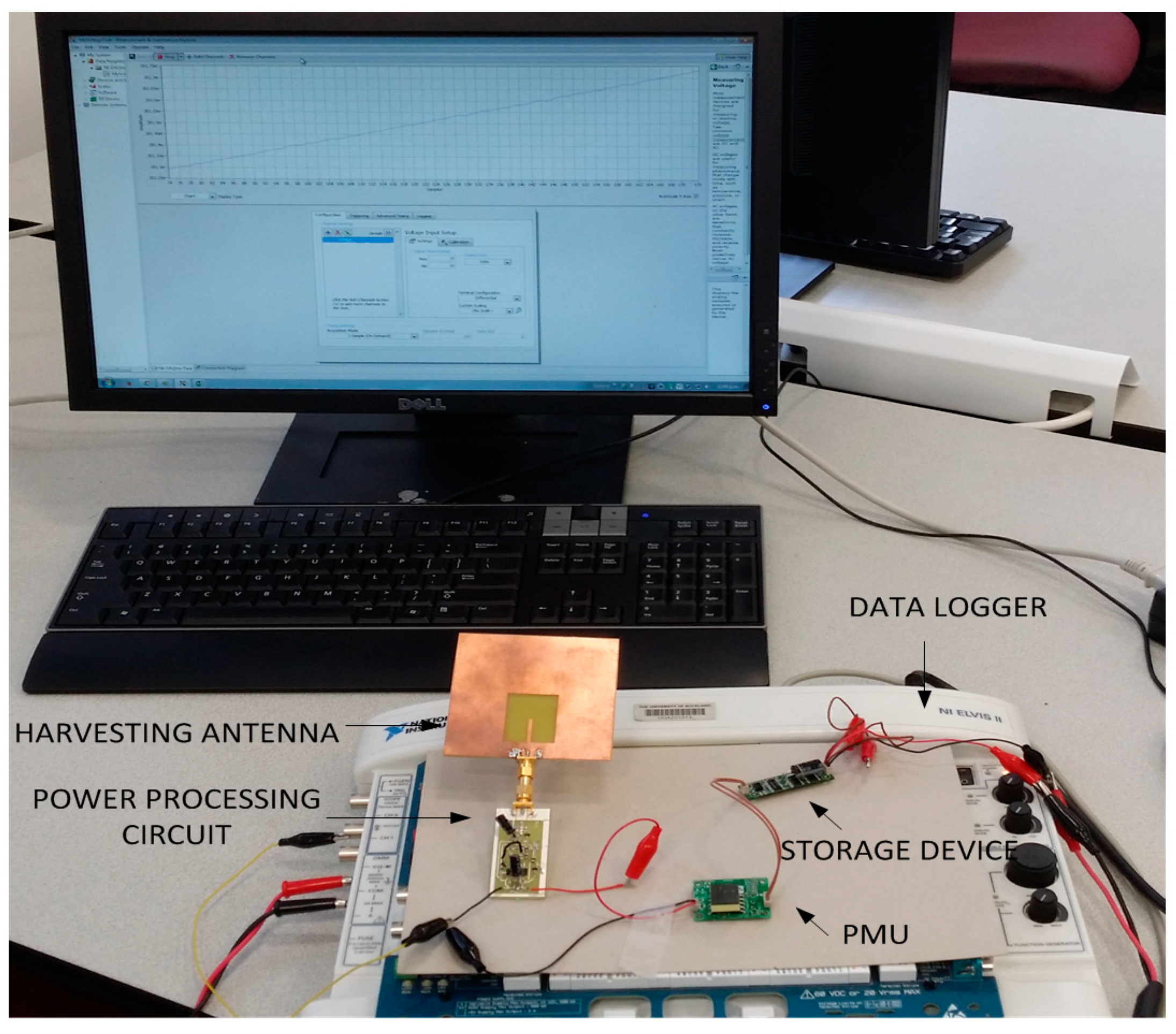
Figure 18.
Measured 2.45 GHz Wi-Fi signal strength inside the indoor area.
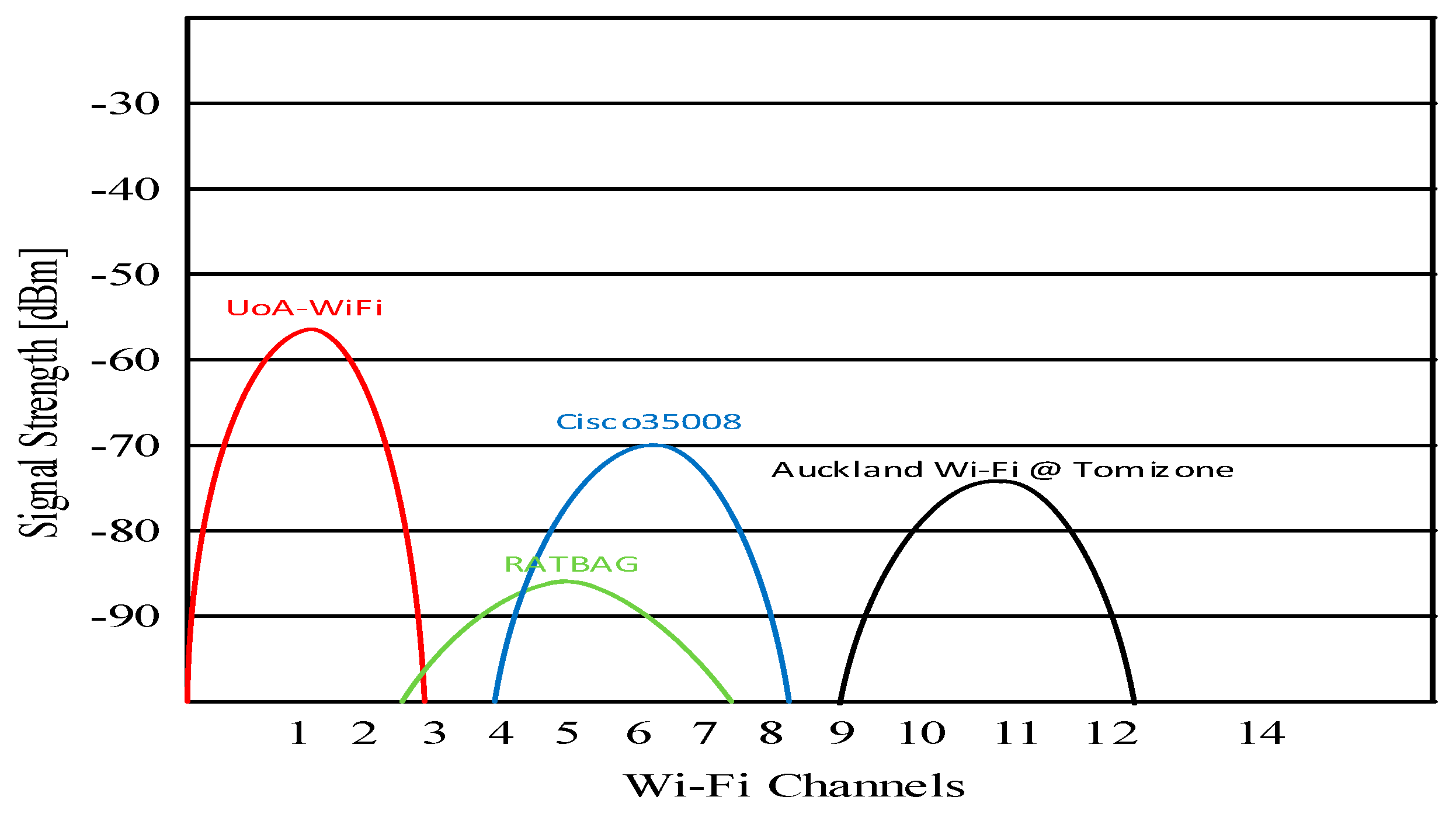
Figure 19.
The actual measurement results, (a) Output voltage, current, power, and energy and (b) The proposed harvesting system efficiency versus time.
Figure 19.
The actual measurement results, (a) Output voltage, current, power, and energy and (b) The proposed harvesting system efficiency versus time.


Table 1.
State of the art wireless sensor power consumption.
| Pcons | 110 nW | 270 nW | 450 nW | 1000 nW |
|---|---|---|---|---|
| Temperature Sensor [1] | Capacitive Sensor [2] | Biomedical Sensor [3] | Actuator Network [4] |
Table 2.
The parameters of Schottky diode.
| Diode | Lp (nH) | Cj (pF) | Cp (pF) | Rs (Ω) | Is (µA) | n |
|---|---|---|---|---|---|---|
| HSMS2850 | 0.4 | 0.18 | 0.09 | 25 | 3 | 1.06 |
| HSMS2860 | 0.4 | 0.18 | 0.09 | 6 | 0.05 | 1.08 |
| HBAT5400 | 2 | 3.0 | 0.08 | 2.4 | 0.1 | 1.00 |
| SMS7621 | 0.2 | 0.1 | 0.05 | 12 | 0.04 | 1.05 |
Table 3.
The proposed circuit components value.
| Parameter | Value | Unit | Parameter | Value | Unit |
|---|---|---|---|---|---|
| L1 | 3.0 | nH | R1, R2 | 510 | kΩ |
| L2 and L3 | 32.0 | nH | R3 | 1 | kΩ |
| C1 | 1.0 | pF | RL | 10 | kΩ |
| C2 | 10 | µF | L4-L6 | 420 | µH |
| C3-C4 | 1.0 | µF | D1-D4 | SMS7621 | - |
| C5, C6 | 4.7 | nF | M1-M4 | ALD210800A | - |
| C7 | 0.47 | µF | PMU | EH5205 | - |
Table 4.
Recent low power wireless sensor characteristics.
| Sensor Spec. | [6] | [15] | [16] | [17] | [18] |
|---|---|---|---|---|---|
| Max.Input Supply (mV) | 1000 | 30–50 | 1000 | 600 | 1200 |
| Power Req. (nW) | 220 | 1.1–6.25 | 190 | 10.8 | 71 |
| Circuit Eqn. Impedance (Ohm) | 6.2 M | 400 k | <50 | - | 2.5 M |
Table 5.
The proposed system key features.
| Single Band | 2.45 GHz, Wi-Fi |
|---|---|
| DC output voltage Using generator for 3 h | |
| Pin = −50 dBm Pin = −40 dBm Pin = −30 dBm Pin = −20 dBm | 50 mV 100 mV 300 mV 400 mV |
| The circuit power consumption Pin = 0 dBm | 18 nW |
| The circuit equivalent impedance | 50 kΩ |
| In indoor environment (RF power density = 0.1 mW/m2) DC output power RF-to-DC conversion efficiency | 3 µW 30% |
Table 6.
System performance comparison.
| Comp | This Work 2016 | [19] 2014 | [20] 2013 | [21] 2010 | [22] 2013 | [23] 2014 |
|---|---|---|---|---|---|---|
| Rect. Topology | Proposed | Series | Series | Series | Doubler | Doubler |
| Rectenna Topology | * | ** | *** | *+ | *++ | *+* |
| No. of RF band | Single | Multi | Single | Double | Double | Five |
| RF bands (GHz) | 2.45 Wi-Fi | 0.9, 1.8, 2.1, 2.45 | 0.45 | 0.9, 1.8 | 0.9, 2.0 | 0.267, 0.4, 0.47, 0.9, 1.35 |
| RF-to-DC Efficiency | 6–30% −20 dBm | 15% −20 dBm | 45% −10 dBm | 4% (for each band) 12 dBm | 9.1% and 8.9% −19 dBm | 19%, 20%, 16%, 5% −10 dBm |
| RF source and distance | Ambient RF | Dedicated RF 50 m | Dedicated 70 cm | Dedicated 3.75 m | - | Dedicated 4 m |
* A bandpass filter for a single frequency; ** Multi-bandpass filter for multiple single frequencies; *** A bandpass filter for multiple single freq; *+ Multi-bandpass filter for multiple single freq. using four-dipole antenna; *++ Multi-bandpass filter for multiple single freq.; no physical connection between two different RF channels; *+* Multi-bandpass filter for multiple single freq.
© 2017 by the authors. Licensee MDPI, Basel, Switzerland. This article is an open access article distributed under the terms and conditions of the Creative Commons Attribution (CC BY) license (http://creativecommons.org/licenses/by/4.0/).
Share and Cite
MDPI and ACS Style
Kadir, E.A.; Hu, A.P. A Power Processing Circuit for Indoor Wi-Fi Energy Harvesting for Ultra-Low Power Wireless Sensors. Appl. Sci. 2017, 7, 827. https://doi.org/10.3390/app7080827
AMA Style
Kadir EA, Hu AP. A Power Processing Circuit for Indoor Wi-Fi Energy Harvesting for Ultra-Low Power Wireless Sensors. Applied Sciences. 2017; 7(8):827. https://doi.org/10.3390/app7080827
Chicago/Turabian StyleKadir, Ermeey Abd, and Aiguo Patrick Hu. 2017. "A Power Processing Circuit for Indoor Wi-Fi Energy Harvesting for Ultra-Low Power Wireless Sensors" Applied Sciences 7, no. 8: 827. https://doi.org/10.3390/app7080827
Note that from the first issue of 2016, this journal uses article numbers instead of page numbers. See further details here.