Article

Manipulating Propagation Constants of Silver Nanowire Plasmonic Waveguide Modes Using a Dielectric Multilayer Substrate

1
Department of Optics and Optical Engineering, Institute of Photonics, University of Science and Technology of China, Hefei 230026, Anhui, China
2
School of Science, Southwest University of Science and Technology, Mianyang 621010, Sichuan, China
3
Center for Fluorescence Spectroscopy, Department of Biochemistry and Molecular Biology, University of Maryland, School of Medicine, Baltimore, MD 21201, USA
*
Author to whom correspondence should be addressed.
This authors contribute equally to this work.
Appl. Sci. 2018, 8(1), 144; https://doi.org/10.3390/app8010144
Submission received: 19 December 2017 / Accepted: 19 December 2017 / Published: 22 January 2018
(This article belongs to the Special Issue Surface Waves on Planar Photonic Crystals)

Abstract

:
Experiments and numerical simulations demonstrate that when a silver nanowire is placed on a dielectric multilayer, but not the commonly used bare glass slide, the effective refractive index of the propagating surface plasmons along the silver nanowire can be controlled. Furthermore, by increasing the thickness of the top dielectric layer, longer wavelength light can also propagate along a very thin silver nanowire. In the experiment, the diameter of the silver nanowire could be as thin as 70 nm, with the incident wavelength as long as 640 nm. The principle of this control is analysed from the existence of a photonic band gap and the Bloch surface wave with this dielectric multilayer substrate.

1. Introduction

During the last decade, there has been a continuous effort toward the development of plasmonic devices. One reason is surface plasmon polaritons (SPPs)—originating from the coupling of an electromagnetic wave to the free electrons of a metal—can strongly confine electromagnetic fields to overcome the optical diffraction limit of dielectric optics, and be very sensitive to the surrounding medium [1,2]. Plasmonic devices are promising to build dense on-chip integrated circuits for next-generation information technology and high-performance nanoscale sensors [3,4,5,6]. Among plasmonic devices, SPP waveguides are one of the key elements. Different configurations have been proposed and verified, and their degree of applicability analysed. For example, a triangular groove milled on a metal surface can work as the channel plasmon subwavelength waveguide [7,8]. Dielectric-loaded SPP waveguides made of a rectangular dielectric rib deposited on a metal film or strip have recently emerged as a potential plasmonic method that can be integrated seamlessly with current silicon-on-insulator photonic circuits, and can sustain the transfer of information at high data rates [9,10,11]. These configurations require top-down nanofabrication. As an alternative, silver nanowires (Ag NWs) synthesized using wet chemistry approaches have proved useful for optical confinement applications below the diffraction limit and for the guiding of light on the nanometre scale, due to their properties of single crystallinity and atomic surface smoothness [12,13,14,15,16,17,18]. There are numerous results on SPP waveguides made of Ag NWs. For example, Ag NW SPP waveguides can also serve as highly directional broadband optical antennas, they can be used to create interferometric logic gates, nanoscale routers, and multiplexers, light modulators, and a complete set of Boolean logic functions [19,20,21,22,23,24,25]. Ag NW plasmonic waveguides have been integrated with planar polymer optical waveguides for the nanoscale confinement and guiding of light on a chip [26]. The photonic and plasmonic interactions between an individual Ag NW and single-layer MoS2 show pronounced nanoscale light–matter interaction between plasmons and atomically thin material that can be exploited for nanophotonic integrated circuits [27]. However, to the best of our knowledge, limited effort has been given to controlling the propagation constants of the plasmonic mode supported by the Ag NW, which is beneficial for active plasmonic devices. The propagating surface plasmons on supported Ag NWs have been tuned with dielectric (Al2O3) layers of different thicknesses. This tunability provides a simple and robust way for the precise routing of optical signals in circuitries and new types of ultrasensitive on-chip optical sensors [28]. The current deposition technique can only coat the Ag NW and its substrate (such as glass slide) simultaneously, and thus the Ag NW will be fixed and cannot be moved to be integrated with other components such as the silicon waveguides. It is not clear that the dielectric layer can be coated uniformly around all surfaces of the NW. The coating of a dielectric layer may destroy the atomically smooth surface of the single-crystal Ag NW, and increase the scattering loss. In this letter, we show that the both the wavenumber (effective refractive index) and propagation distance or cut off wavelength of the SPP waveguide with the Ag NW can be tuned by placement on a dielectric multilayer as the substrate.

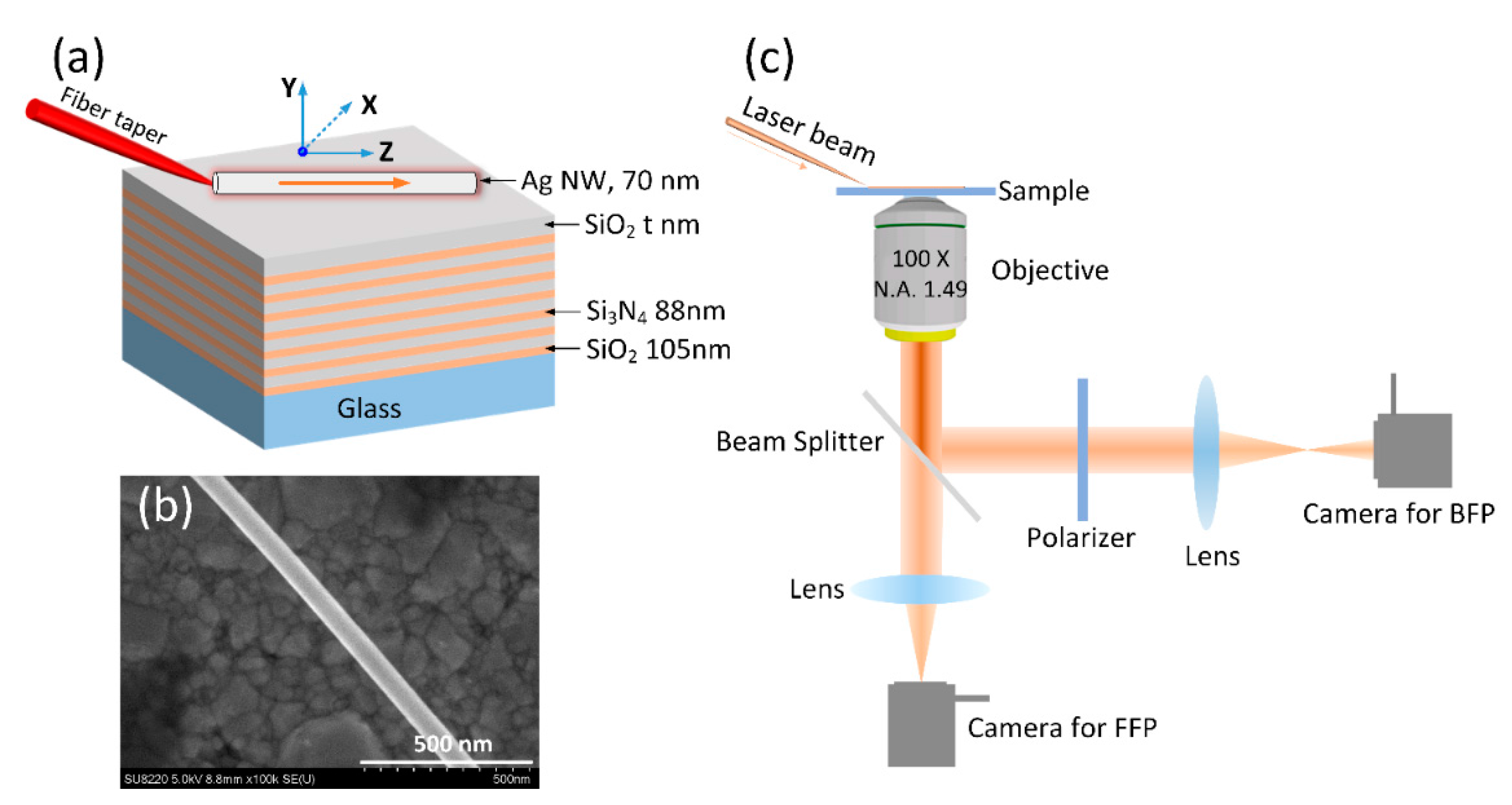
2. Materials and Methods
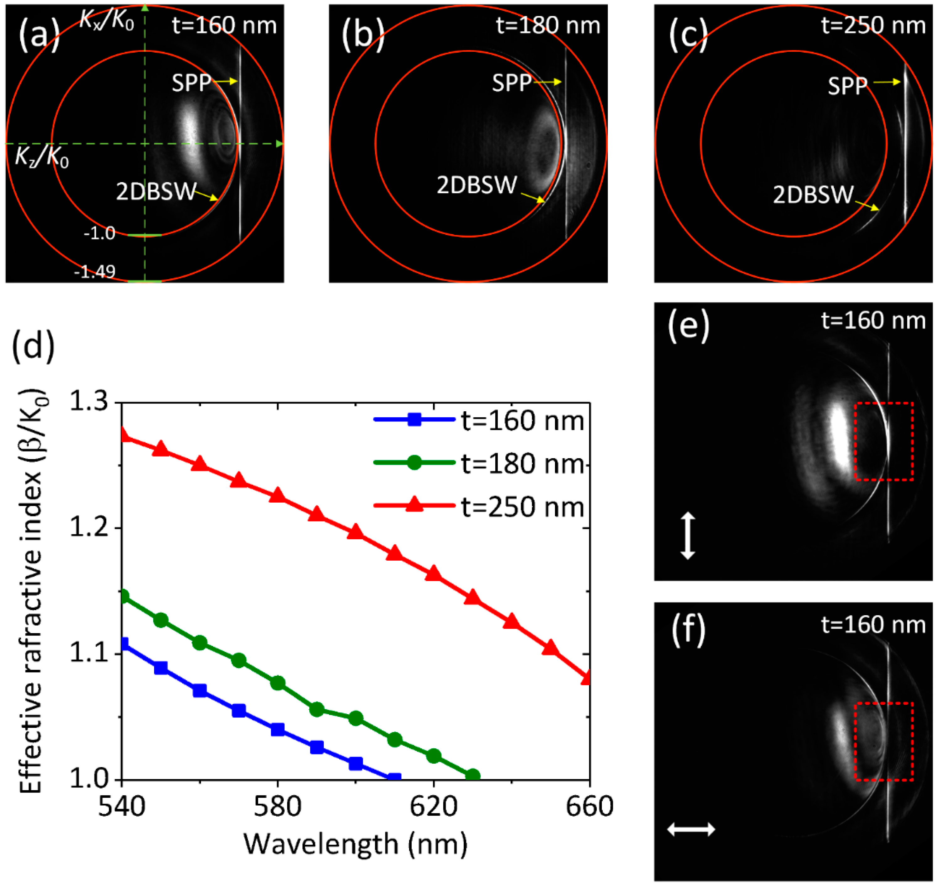
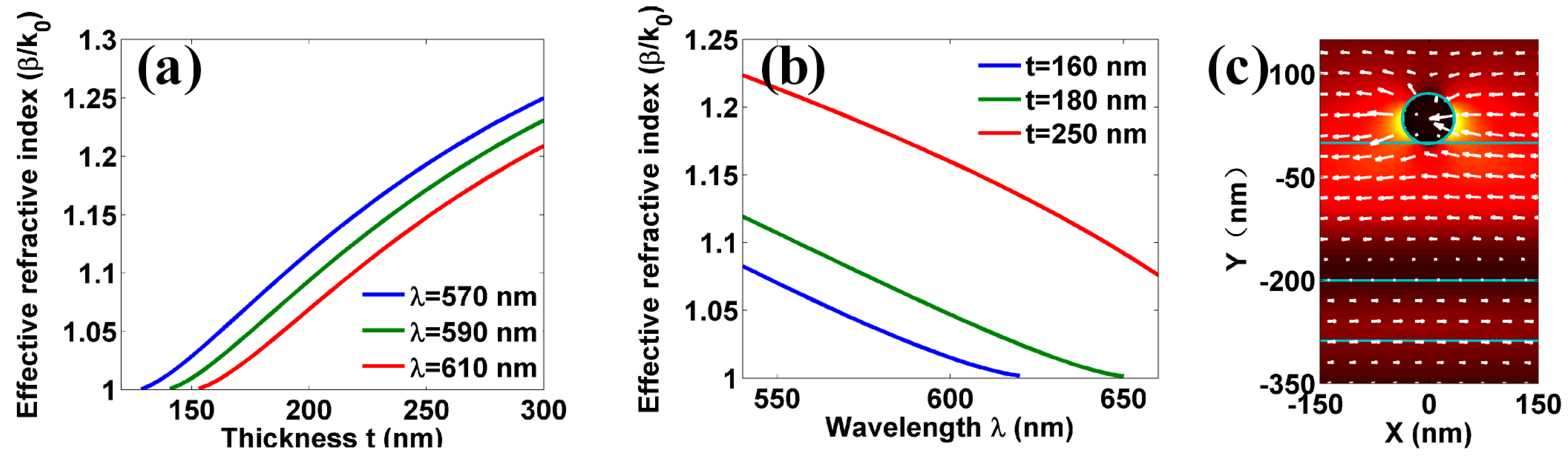
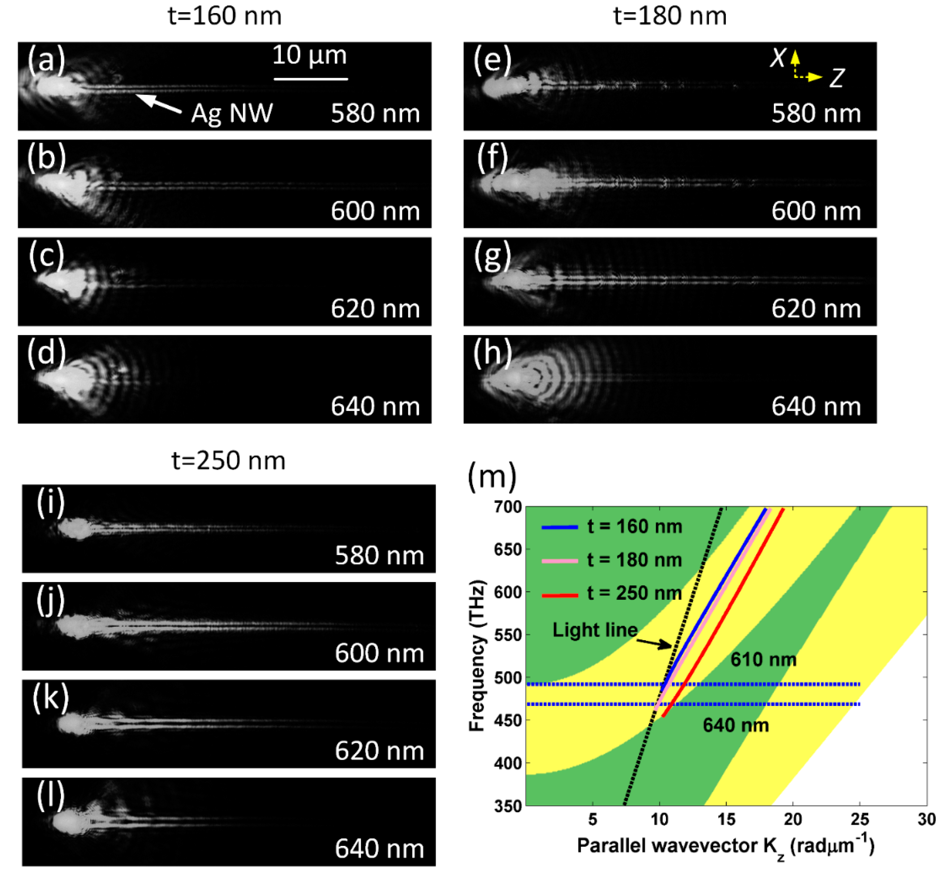
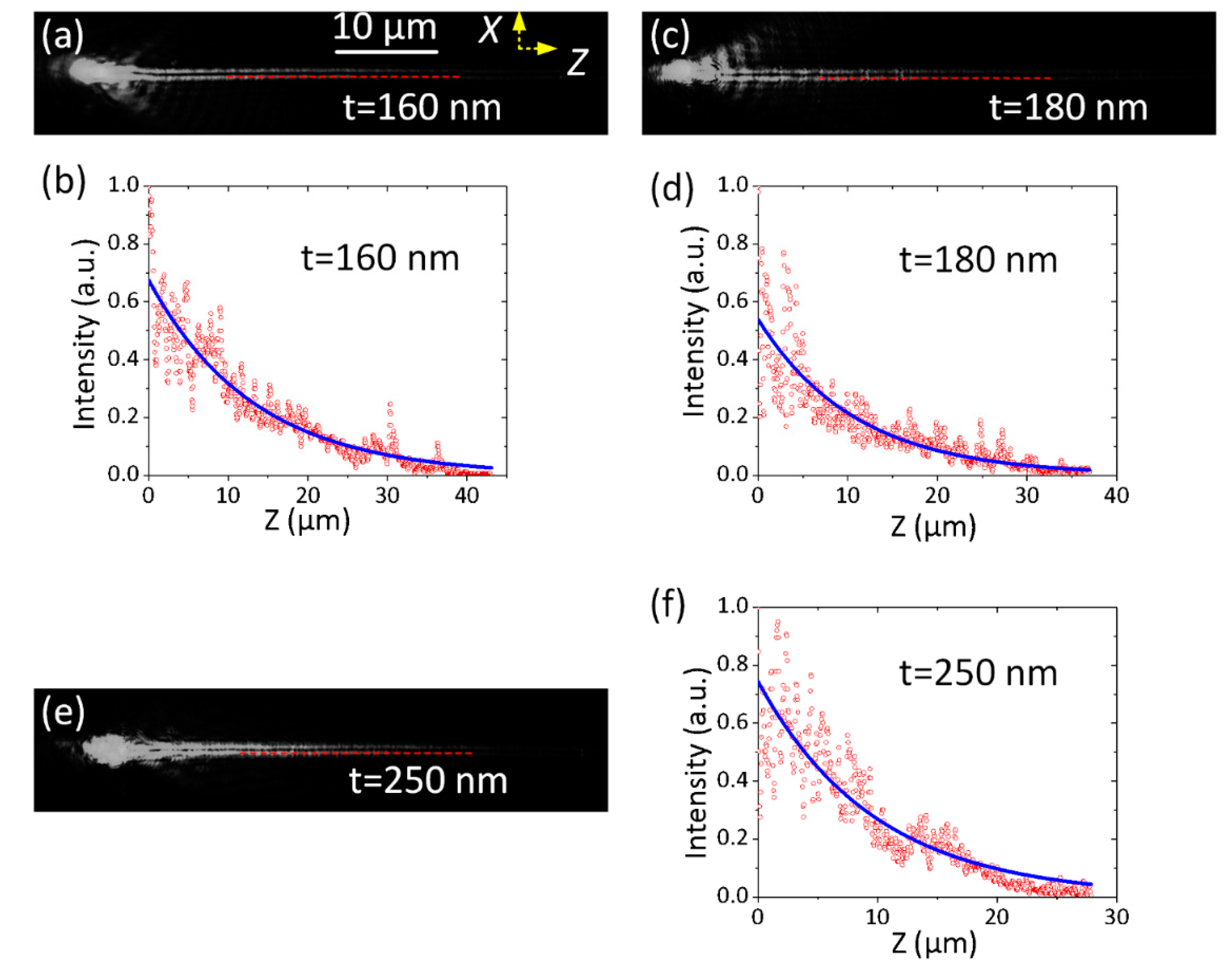
The schematic of the sample is shown in Figure 1a. The dielectric multilayer (made of alternating SiO2 and Si3N4 layers) was fabricated using plasma-enhanced chemical vapour deposition. The thicknesses of SiO2 and Si3N4 were 105 and 88 nm, respectively. The thickness of the top SiO2 layer is defined as t nm, which will be varied in the following experiments and simulations. An Ag NW with a diameter of approximately 70 nm was deposited on this multilayer (Figure 1b). The Ag NW was purchased from XFNANO Materials Tech Co., Ltd., Nanjing, China. A laser beam (from a SuperK supercontinuum source, NKT Photonics, Birkerød, Denmark) was used for excitation; it was first lens-coupled into a standard single-mode silica fibre, and its taper would be brought into contact with the Ag NW by a micromanipulator. As a result, the laser beam can be coupled into the Ag NW. The beam propagating along this NW was characterized by a home-built instrument for leakage radiation microscopy (LRM). A schematic of the experimental setup (LRM) is shown in Figure 1c. This LRM can collect both the front focal plane (FFP) and the back focal plane (BFP) images, which can be used to derive the propagation constants (β + i*β’) of the SPP propagating along the Ag NW. β/K0 is the effective refractive index of the plasmonic mode, and the imaginary part (β’) represents the propagation loss. Details of image formation on the FFP and BFP, and how to derive the embedded optical information from the BFP and FFP images, can be found in references [29,30,31,32,33].

3. Results

In this experiment, three dielectric-multilayer substrates were fabricated, with the top layer thickness (t) selected at about 160, 180, and 250 nm. The thicknesses of the other layers were kept the same as shown in Figure 1a. By using this dielectric multilayer substrate, SPPs can propagate for a long distance along the thin Ag NW (such as diameter of the Ag NW is less than 100 nm). However, if the same Ag NW was placed on a glass substrate, the propagation distance would be much shorter [34]. Figure 2a–c show the BFP images when the Ag NW of 70 nm diameter was placed on these three substrates. The incident wavelength was selected as 590 nm. In our LRM, an oil-immersed objective with numerical aperture (NA) at 1.49 was used to collect the leakage plasmonic signals. The outer red rings on Figure 2a–c represent the largest collection angle that can be derived as arcsin (1.49/1.515) = 79.58°, where the refractive index of the oil is 1.515. The inner ring represents the critical angle where the total internal reflection occurs, hence the bright areas inside this inner ring are due to the direct transmission of the light through the dielectric multilayer. On the BFP images, the bright vertical line labelled with SPP is the signature of the SPP propagating along the Ag NW [32], and the line is parallel to the axis Kx/K0, which is perpendicular to the NW long axis. From the distance (D) between this vertical line and the axis (Kx/K0), the diameter of the outer ring (R) and known NA (1.49) of the objective, the effective refractive index (or wavenumber, or the real part of the propagation constant) β/K0 of this SPP waveguide mode can be calculated with the equation β/K0 = (D/R)*NA, where the K0 is the wavenumber of the light in vacuum. The SPP propagates along the Z-axis, and the wavenumber along the Z-direction is Kz/K0 = β/K0 = 1.03 (a), 1.05 (b), and 1.21 (c), respectively. The BFP images at additional wavelengths ranging from 540 to 660 nm were also captured, such as the BFP images at 570 and 610 nm wavelength, which were used to derive the curves of the effective refractive index vs. incident wavelength, as shown in Figure 2d. With the increasing of incident wavelength, the effective index decreases, and at all these wavelengths, the effective index will be increased if the top layer thickness is increased from 160 to 250 nm. These results clearly demonstrate that the effective index of SPP waveguides mode can be tuned with the thickness (t) of the top SiO2 layer (Figure 1a).
There are bright arcs on the BFP images (labelled with 2DBSW) appearing close to the bright lines, which are the two-dimensional Bloch Surface Waves (2DBSW) generated by the light from fibre taper. The 2DBSW is the two-dimensional surface wave spreading on the surface of the dielectric multilayer. To test the polarization of these modes (2DBSW and of the NW), a linear polarizer was placed before the camera for BFP images, and the corresponding images with two orientations of the polarizer are shown in Figure 2e,f. These two images (the area marked with the dotted box) show that the 2DBSW is of transverse electronic (TE) polarization, meaning that the polarization direction of the light on the bright arc is perpendicular to the radial direction of the arc, similar to the azimuthal polarization of a vortex beam [35]. For the vertical bright line, the light spot on this line with Kx/K0 = 0 is dark in the case of horizontal polarization (Figure 2f), and is bright in the case of perpendicular polarization (Figure 2e); this phenomenon reveals that the polarization direction of this light spot is along this bright line, and therefore this mode is the H1X mode [36]. Numerical simulations using the finite element method were also carried out to demonstrate the effect of top layer thickness and wavelengths on the effective refractive index. The permittivity of Ag NWs at different wavelengths were based on experimental values [37]. Due to the surface scattering and grain boundary effects in real thin films in the simulations, the refractive indices of SiO2 and Si3N4 were nSiO2 = 1.46 + i10−3 and nSi3N4 = 2.14 + i5 × 10−3, respectively. The refractive index of the glass substrate was nglass = 1.515. The thickness of each dielectric layer was the same as that shown in Figure 1a. Figure 3a demonstrates the calculated effective refractive index of plasmonic H1X mode as a function of the top layer thicknesses with three incident wavelengths (570, 590, and 610 nm—identical to those used on the BFP images in Figure 2). The diameter of the nanowire is 70 nm. The simulation results show that the effective refractive index (β/k0) of the H1X mode is decreased with decreasing top layer thickness, which is consistent with the results derived from the BFP images on Figure 2a–c. As the wavelength decreased, the cutoff thickness of H1X mode also decreased. For example, when the incident wavelength was 610 nm, this mode disappeared, as the top layer thickness was less than 160 nm. Whereas at a 570-nm wavelength, the same mode disappeared at a top layer thickness of 130 nm. To understand the wave guide behaviour of H1X mode placed on the dielectric multilayer, the electric field distribution of the H1X mode was calculated and shown in Figure 3c. Different from the case of the nanowire placed on the glass substrate, the predominantly electric field energy of H1X mode of the nanowire was localized near the top layer of dielectric multilayer. The changes of the top layer thickness can adjust the field localization of H1X mode, and greatly affect the wave guiding behaviour of this H1X mode. Figure 3b shows the effective refractive index of H1X mode at three different top layer thicknesses (t = 160, 180, and 250 nm, the same as those used in the experiment) as a function of the incident wavelength. As expected, the change of the effective refractive index with the incident wavelength is consistent with the experimental results shown in Figure 2d. At all three thicknesses, the index decreased with the increasing of the incident wavelength from 540 to 660 nm.
Figure 3b also reveals another interesting phenomenon; with increasing top layer thickness, the cutoff wavelength for this H1X mode will be increased. For example, when the top layer thickness is t = 160 nm, this mode will be cut off with the incident wavelength longer than 620 nm, whereas when the thickness is increased into 250 nm, this mode can also appear when the incident wavelength is 660 nm. In our experiment, FFP images of the plasmon propagating along this 70 nm diameter Ag NW at different wavelengths and top layer thicknesses are shown in Figure 4. The selected wavelengths were 580, 600, 620, and 640 nm. Figure 4a–d shows the top layer thickness was approximately 160 nm, and it is clear that at 620 nm wavelength, we could barely find the plasmon propagating along the Ag NW. On the contrary, in Figure 4i–l, the top layer was at the thickness of approximately 250 nm, and the plasmon could be clearly observed propagating along the NW even if the wavelength was 640 nm. Experiments and simulations verified that the top layer thickness can be used to tune the cutoff wavelength of the plasmonic H1X mode on the Ag NW.
To further confirm the mechanism of the above phenomena, the projected photonic band structure of the dielectric multilayer for transverse electronic (TE) polarization was simulated as shown in Figure 4m [38]. The dispersion relations of H1X mode at the three top layer thicknesses were also plotted in this figure. The three curves (t = 160, 180, and 250 nm) of the dispersive (dispersion) relations are all located inside the stop band gap (the yellow zone on Figure 4m) of this multilayer and lie on the right side of the light line, which is the fundamental reason that the plasmons can be confined and propagate along this very thin Ag NW. As shown in Figure 4m, we can locate the cutoff wavelength for the plasmonic mode, which decreases with the decreasing of the top layer thickness. This phenomenon also can be analysed from the change of effective index of the plasmonic mode with the incident wavelength and top layer thickness. As shown in Figure 2 and Figure 3, in the case of a thin top dielectric layer (e.g., t = 160 nm), its refractive index is smaller than that of a thicker one (t = 250 nm), and with the increasing of the incident wavelength, the refractive index of this SPP mode will decrease accordingly. When this index approaches 1.0, this mode will be cut off. It is easy to understand that the SPP mode on the top layer with t = 160 nm has a shorter cutoff incident wavelength.
It should be noted that the imaginary part (β’) of the propagation constant represents the propagation distance of this plasmonic mode, and from Figure 4, it is evident that the top dielectric layers affect the propagation distance. As an example, the propagation distances of the SPPs along the Ag NW placed on three multilayer substrates have been fitted and derived as shown in Figure 5. The incident wavelength was fixed at 590 nm, and the thickness of the top SiO2 layer was selected as t = 160 nm, t = 180 nm, and t = 250 nm, respectively. The thicknesses of the other 13 layers were kept the same as shown in Figure 1a. It is clearly shown that, although the incident wavelength and diameter of the Ag NW were both the same on the three multilayer substrates, the propagation distances were different from each other. The propagation distances of the plasmonic mode were derived as 13 μm (at t = 160 nm), 11 μm (at t = 180 nm), and 10 μm (at t = 250 nm), respectively.

4. Conclusions

In conclusion, a new method has been proposed to mediate the propagation constant of the SPP mode on a very thin Ag NW (diameter as low as 70 nm), when placed on a dielectric multilayer. Both the effective refractive index and propagation distance or cutoff wavelength of this mode can be tuned with the thickness of the top dielectric (SiO2) layer. When the Ag NW of the same diameter was placed on a commonly used glass or silicon substrate, the SPP mode here (H1X mode or plasmonic leaky mode) disappeared, and only the plasmonic bound mode could remain, but with very short propagation distance [34]. With this method, the Ag NW can be placed on any location of the substrate and can be moved flexibly to be integrated with other components. There is no need to coat another surface cladding, and will avoid damaging the smooth NW surface. For future applications, the top SiO2 layer can be replaced with a layer made of piezoelectric materials, such as LiNbO3, whose thickness or refractive index can be tuned with external electric signals, providing an approach for realizing active nano-devices. This tuning of the effective refractive index and propagation distance of the SPP waveguide modes on an Ag NW can be used to understand a serial of Boolean logic functions in on-chip integrated circuits for next-generation information technology and nanoscale optical sensing. We note that the field intensity is stronger confined near the NW surface Figure 3e. This confinement will result in a small observed volume, which is of interest for biophotonic applications [39,40,41,42].

Acknowledgments

This work was supported by MOST (2013CBA01703 and 2016YFA0200601), NSFC (61427818, 11774330 and 11374286), and the Science and Technological Fund of Anhui Province for Outstanding Youth (1608085J02), and the Longshan academic talent research supporting program of SWUST (17LZX626). This work was also supported by grants from the National Institute of Health (GM107986, EB006521, EB018959, and OD019975). This work was partially carried out at the University of Science and Technology of China’s Centre for Micro and Nanoscale Research and Fabrication. We thank Xiaolei Wen, Linjun Wang and Yu Wei for their help on the micro/nano fabrication steps.

Author Contributions

D.G.Z conceived the idea and drafted the manuscript. Y.X. carried out the optical experiments. J.C. and X.T. performed the numerical calculations. R.W., F.L., and Y.K. fabricated the dielectric multilayer. J.R.L., R.B., M.R., P.W. and H.M. assisted in drafting the manuscript. All authors discussed the results and contributed to the writing and editing of the manuscript. Y.X. and J.C. contributed equally to this work.

Conflicts of Interest

The authors declare no competing financial interests.

References

  1. Raether, H. Surface Plasmons on Smooth and Rough Surfaces and on Gratings; Springer: Berlin, Germany, 1988. [Google Scholar]
  2. Barnes, W.L.; Dereux, A.; Ebbesen, T.W. Surface Plasmon Subwavelength Optics. Nature 2003, 424, 824–830. [Google Scholar] [CrossRef]
  3. Ebbesen, T.W.; Genet, C.; Bozhevolnyi, S.I. Surface-Plasmon Circuitry. Phys. Today 2008, 61, 44–50. [Google Scholar] [CrossRef]
  4. Gramotnev, D.K.; Bozhevolnyi, S.I. Plasmonics beyond the Diffraction Limit. Nat. Photonics 2010, 4, 83–91. [Google Scholar] [CrossRef]
  5. Lal, S.; Link, S.; Halas, N.J. Nano-Optics from Sensing to Waveguiding. Nat. Photonics 2007, 1, 641–648. [Google Scholar]
  6. Maier, S.A. Plasmonics: Fundamentals and Applications; Springer: New York, NY, USA, 2007. [Google Scholar]
  7. Bozhevolnyi, S.I.; Volkov, V.S.; Devaux, E.; Laluet, J.Y.; Ebbesen, T.W. Channel Plasmon Subwavelength Waveguide Components Including Interferometers and Ring Resonators. Nature 2006, 440, 508–511. [Google Scholar] [CrossRef]
  8. Pile, D.F.P.; Gramotnev, D.K. Channel Plasmon—Polariton in a Triangular Groove on a Metal Surface. Opt. Lett. 2004, 29, 1069–1071. [Google Scholar] [PubMed]
  9. Hassan, K.; Bouhelier, A.; Bernardin, T.; Colas-des-Francs, G.; Weeber, J.-C.; Dereux, A. Momentum-Space Spectroscopy for Advanced Analysis of Dielectric-Loaded Surface Plasmon Polariton Coupled and Bent Waveguides. Phys. Rev. B 2013, 87, 195428. [Google Scholar] [CrossRef]
  10. Grandidier, J.; Massenot, S.; Colas des Francs, G.; Bouhelier, A.; Weeber, J.-C.; Markey, L.; Dereux, A. Dielectric-Loaded Surface Plasmon Polariton Waveguides: Figures of Merit and Mode Characterization by Image and Fourier Plane Leakage Microscopy. Phys. Rev. B 2008, 78, 245419. [Google Scholar] [CrossRef]
  11. Massenot, S.; Grandidier, J.; Bouhelier, A.; Colas des Francs, G.; Markey, L.; Weeber, J.-C.; Dereux, A.; Renger, J.; Gonzàlez, M.U.; Quidant, R. Polymer-Metal Waveguides Characterization by Fourier Plane Leakage Radiation Microscopy. Appl. Phys. Lett. 2007, 91, 243102. [Google Scholar]
  12. Rycenga, M.; Cobley, C.M.; Zeng, J.; Li, W.Y.; Moran, C.H.; Zhang, Q.; Qin, D.; Xia, Y.N. Controlling The Synthesis and Assembly of Silver Nanostructures for Plasmonic Applications. Chem. Rev. 2011, 111, 3669–3712. [Google Scholar]
  13. Sun, Y.G.; Xia, Y.N. Large-Scale Synthesis of Uniform Silver Nanowires through A Soft, Self-Seeding, Polyol Process. Adv. Mater. 2002, 14, 833–837. [Google Scholar] [CrossRef]
  14. Dickson, R.M.; Lyon, L.A. Unidirectional plasmon propagation in metallic nanowires. J. Phys. Chem. B 2000, 104, 6095–6098. [Google Scholar]
  15. Li, M.; Zou, C.L.; Ren, X.F.; Xiong, X.; Cai, Y.J.; Guo, G.P.; Tong, L.M.; Guo, G.C. Transmission of Photonic Quantum Polarization Entanglement in A Nanoscale Hybrid Plasmonic Waveguide. Nano Lett. 2015, 15, 2380–2384. [Google Scholar] [CrossRef] [PubMed]
  16. Wang, W.H.; Yang, Q.; Fan, F.R.; Xu, H.X.; Wang, Z.L. Light Propagation in Curved Silver Nanowire Plasmonic Waveguides. Nano Lett. 2011, 11, 1603–1608. [Google Scholar] [CrossRef] [PubMed]
  17. Sanders, A.W.; Routenberg, D.A.; Wiley, B.J.; Xia, Y.N.; Dufresne, E.R.; Reed, M.A. Observation of Plasmon Propagation, Redirection, and Fan-Out in Silver Nanowires. Nano Lett. 2006, 6, 1822–1826. [Google Scholar] [CrossRef] [PubMed]
  18. Shegai, T.; Huang, Y.; Xu, H.X.; Kall, M. Coloring Fluorescence Emission with Silver Nanowires. Appl. Phys. Lett. 2010, 96, 103114. [Google Scholar] [CrossRef]
  19. Yan, R.X.; Pausauskie, P.; Huang, J.X.; Yang, P.D. Direct Photonic-Plasmonic Coupling and Routing in Single Nanowires. Proc. Natl. Acad. Sci. USA 2009, 106, 21045–21050. [Google Scholar] [CrossRef] [PubMed]
  20. Lal, S.; Hafner, J.H.; Halas, N.J.; Link, S.; Nordlander, P. Noble Metal Nanowires: From Plasmon Waveguides to Passive and Active Devices. Acc. Chem. Res. 2012, 45, 1887–1895. [Google Scholar] [CrossRef] [PubMed]
  21. Wei, H.; Li, Z.P.; Tian, X.R.; Wang, Z.X.; Cong, F.Z.; Liu, N.; Zhang, S.P.; Nordlander, P.; Halas, N.J.; Xu, H.X. Quantum Dot-Based Local Field Imaging Reveals Plasmon-Based Interferometric Logic in Silver Nanowire Networks. Nano Lett. 2011, 11, 471–475. [Google Scholar] [CrossRef] [PubMed]
  22. Fang, Y.R.; Li, Z.P.; Huang, Y.Z.; Zhang, S.P.; Nordlander, P.; Halas, N.J.; Xu, H.X. Branched Silver Nanowires as Controllable Plasmon Routers. Nano Lett. 2010, 10, 1950–1954. [Google Scholar] [CrossRef] [PubMed]
  23. Shegai, T.; Miljkovic, V.D.; Bao, K.; Xu, H.X.; Nordlander, P.; Johansson, P.; Kall, M. Unidirectional Broadband Light Emission from Supported Plasmonic Nanowires. Nano Lett. 2011, 11, 706–711. [Google Scholar] [CrossRef] [PubMed]
  24. Wei, H.; Wang, Z.; Tian, X.; Kall, M.; Xu, H. Cascaded Logic Gates in Nanophotonic Plasmon Networks. Nat. Commun. 2011, 2, 387. [Google Scholar] [CrossRef] [PubMed]
  25. Cao, L.N.; Nome, R.A.; Montgomery, J.M.; Gray, S.K.; Scherer, N.F. Controlling Plasmonic Wave Packets in Silver Nanowires. Nano Lett. 2010, 10, 3389–3394. [Google Scholar] [CrossRef] [PubMed]
  26. Pyayt, A.L.; Wiley, B.; Xia, Y.N.; Chen, A.T.; Dalton, L. Integration of Photonic and Silver Nanowire Plasmonic Waveguides. Nat. Nanotechnol. 2008, 3, 660–665. [Google Scholar] [CrossRef] [PubMed]
  27. Goodfellow, K.M.; Beams, R.; Chakraborty, C.; Novotny, L.; Vamivakas, A.N. Integrated Nanophotonics Based on Nanowire Plasmons and Atomically-Thin Material. Optica 2014, 1, 149–152. [Google Scholar] [CrossRef]
  28. Wei, H.; Zhang, S.P.; Tian, X.R.; Xu, H.X. Highly Tunable Propagating Surface Plasmons on Supported Silver Nanowires. Proc. Natl. Acad. Sci. USA 2013, 110, 4494–4499. [Google Scholar]
  29. Song, M.; Bouhelier, A.; Bramant, P.; Sharma, J.; Dujardin, E.; Zhang, D.; Colas-des-Francs, G. Imaging Symmetry-Selected Corner Plasmon Modes in Penta-Twinned Crystalline Ag Nanowires. ACS Nano 2011, 5, 5874–5880. [Google Scholar] [CrossRef] [PubMed]
  30. Drezet, A.; Hohenau, A.; Koller, D.; Stepanov, A.; Ditlbacher, H.; Steinberger, B.; Aussenegg, F.R.; Leitner, A.; Krenn, J.R. Leakage Radiation Microscopy of Surface Plasmon Polaritons. Mater. Sci. Eng. B 2008, 149, 220–229. [Google Scholar] [CrossRef]
  31. Yang, H.B.; Qiu, M.; Li, Q. Identification and Control of Multiple Leaky Plasmon Modes in Silver Nanowires. Laser Photonics Rev. 2016, 10, 278–286. [Google Scholar] [CrossRef]
  32. Wang, Z.X.; Wei, H.; Pan, D.; Xu, H.X. Controlling The Radiation Direction of Propagating Surface Plasmons on Silver Nanowires. Laser Photonics Rev. 2014, 8, 596–601. [Google Scholar] [CrossRef]
  33. Jia, Z.L.; Wei, H.; Pan, D.; Xu, H.X. Direction-Resolved Radiation from Polarization-Controlled Surface Plasmon Modes on Silver Nanowire Antennas. Nanoscale 2016, 8, 20118–20124. [Google Scholar] [CrossRef] [PubMed]
  34. Zhang, D.G.; Xiang, Y.F.; Chen, J.X.; Cheng, J.J.; Zhu, L.F.; Wang, R.X.; Zou, G.; Wang, P.; Ming, H.; Rosenfeld, M.; et al. Extending the Propagation Distance of a Silver Nanowire Plasmonic Waveguide with a Dielectric Multilayer Substrate. Nano Lett. 2018. [Google Scholar] [CrossRef] [PubMed]
  35. Zhan, Q.W. Cylindrical Vector Beams: From Mathematical Concepts to Applications. Adv. Opt. Photonics 2009, 1, 1–57. [Google Scholar] [CrossRef]
  36. Zhang, S.P.; Xu, H.X. Optimizing Substrate-Mediated Plasmon Coupling toward High-Performance Plasmonic Nanowire Waveguides. ACS Nano 2012, 6, 8128–8135. [Google Scholar] [CrossRef] [PubMed]
  37. Palik, E.D.; Ghosh, G. Handbook of Optical Constants of Solids; Academic Press: Cambridge, MA, USA, 1998. [Google Scholar]
  38. Joannopoulos, J.D.; Johnson, S.G.; Winn, J.N.; Meade, R.D. Photonic Crystals: Molding the Flow of Light; Princeton University Press: Princeton, NJ, USA, 2008. [Google Scholar]
  39. Gerard, D.; Wenger, J.; Devilez, A.; Gachet, D.; Stout, B.; Bonod, N.; Popov, E.; Rigneault, H. Strong Electromagnetic Confinement near Dielectric Microspheres to Enhance Single-Molecule Fluorescence. Opt. Express 2008, 16, 15297–15303. [Google Scholar] [CrossRef] [PubMed]
  40. Estrada, L.C.; Martinez, O.E.; Brunstein, M.; Bouchoule, S.; Le-Gratiet, L.; Talneau, A.; Sagnes, I.; Monnier, P.; Levenson, J.A.; Yacomotti, A.M. Small volume Excitation of Dye Fluorescence on a 2D Photonic Crystal Surface. Opt. Express 2010, 18, 3693–3699. [Google Scholar] [CrossRef] [PubMed]
  41. Wenger, J.; Gerard, D.; Aouani, H.; Rigneault, H.; Lowder, B.; Blair, S.; Devaux, E.; Ebbesen, T.W. Nanoaperture-Enhanced Singla-to-Noise Ratio in Fluorescence Correlation Spectroscopy. Anal. Chem. 2009, 81, 834–839. [Google Scholar] [CrossRef] [PubMed]
  42. Estrada, L.C.; Aramendia, P.F.; Martinez, O.E. 10000 times Reduction for Fluorescence Correlation Spectroscopy Using Nano-Antenna. Opt. Express 2008, 16, 20597–20602. [Google Scholar] [CrossRef] [PubMed]
Figure 1. Schematic illustration of the sample. (a) The silver nanowire (Ag NW) was placed on a dielectric multilayer consisting of alternating layers of SiO2 (105-nm-thick) and Si3N4 (88-nm-thick). There were fourteen layers in total, with a top SiO2 layer with a varied thickness of t nm. A fibre taper was used to couple the laser beam into the nanowire. The NW was oriented along the Z-axis and perpendicular to the X-axis; (b) SEM image of the Ag NW (diameter of 70 nm); (c) Schematic of the experimental set-up for imaging the plasmon’s propagation along the Ag NW. Two cameras are used for capturing the front focal plane (FFP) and back focal plane (BFP) images. A polarizer can be used to check the polarization state of this plasmonic mode.
Applsci 08 00144 g001
Figure 2. Controlling the effective refractive index of the surface plasmon polariton (SPP) waveguide mode with the top dielectric (SiO2) layer’s thickness. The thickness was selected as t = 160, 180, and 250 nm, respectively. The incident wavelength was selected as 590 nm. (ac) the corresponding BFP images; (d) the curves of effective refractive index vs. the incident wavelength in the case of three top layer thicknesses; (e,f) BFP images in the case of t = 160 nm with a polarizer before the detector. The white double arrowhead lines represent the direction of the polarizer. On (ac), the red rings with diameters at 1.49 and 1 are given by the numerical aperture (NA) of the objective and the critical angle, respectively.
Applsci 08 00144 g002
Figure 3. Simulated effective refractive index of the SPP waveguide mode. (a) The effective refractive index of Bloch surface wave mode versus the thickness of top SiO2 layer, in the case of three selected incident wavelengths (570, 590, and 610 nm); (b) The effective refractive index of BSW mode versus the incident wavelength with three different thicknesses of top SiO2 layer; (c) The electric field distribution of H1X mode with thickness t = 200 nm and wavelength λ = 590 nm. The arrows with white colour denote the directions of the electric fields, which shows that the mode is the H1X mode. The diameter of the Ag nanowire was 70 nm.
Applsci 08 00144 g003
Figure 4. Controlling the propagation distance of the SPP waveguide mode with the top SiO2 layer’s thickness. (ad) The thickness of the top dielectric layer is t = 160 nm; (eh) the thickness of the top dielectric layer is t = 180 nm; (il) the thickness of the top dielectric layer is 250 nm. The incident wavelength varied from 580 to 640 nm with 20 nm step, as labelled from (a) to (l). The scale bar in (a) is also applicable for the images in (bl). The dimeter of the Ag NW was about 70 nm in all these images; (m) Simulated band structure of the multilayer and dispersion relation of the SPP waveguide mode. The projected photonic band structure of the dielectric multilayer for transverse electronic (TE) polarization. The yellow zone denotes the stop band. The solid lines denote the dispersion relations of BSW modes with different thickness of the top SiO2 layer (t = 160, 180, and 250 nm).
Applsci 08 00144 g004
Figure 5. FFP images of the plasmon’s propagations. Three Ag NWs of the same diameter (about 70 nm) were put on three substrates with different thickness of the top SiO2 layer. The top SiO2 layer’s thickness was (a,b) t = 160 nm; (c,d) t = 180 nm, and (e,f) t = 250 nm, respectively. The incident wavelength was selected as 590 nm. On (b,d,f), the blue solid line is an exponential fit to the data (red dots) and was used to extract the propagation distance of the plasmonic mode as 13 μm (at t = 160 nm), 11 μm (at t = 180 nm), and 10 μm (at t = 250 nm). The scale bar in (a) is also applicable for (c,e).
Applsci 08 00144 g005

