Theoretical Assessment of DC/DC Power Converters’ Basic Topologies. A Common Static Model


Departamento de Ingeniería Electrónica, de Sistemas Informáticos y Automática, University of Huelva, Campus “La Rábida”, 21819 – La Rábida, Huelva Spain
*
Author to whom correspondence should be addressed.
Appl. Sci. 2018, 8(1), 19; https://doi.org/10.3390/app8010019
Submission received: 19 November 2017
/
Revised: 11 December 2017
/
Accepted: 18 December 2017
/
Published: 23 December 2017
Abstract
:Featured Application
DC/DC converters design and teaching.
Abstract
By the application of well-known circuit analysis techniques, this paper develops an intuitive approach to model the steady state regime of the three DC/DC power converters’ basic topologies (buck, boost and buck-boost). The developed approach can be considered new, realistic, accurate, general and practical. The approach is new because it is not present in the literature; realistic because it considers the main non-idealities of the different passive and active components that make up the converters; accurate because its theoretical results fit properly to those obtained in actual converters; general because it is valid for the three basic topologies; and practical because its applicability is easy and immediate from the data sheets of the converters’ components (no measurements are needed). The developed model transforms a complex system with strong non-idealities in the form of distributed parameters, in a simple and intuitive scheme of concentrated parameters (just three), which accurately reflects the actual behavior of the three basic converters’ topologies. The characteristic parameters of the model and its main relationships are determined analytically. The quality of the developed approach has been tested in the paper and can be considered excellent.
1. Introduction
The simplified study of allegedly ideal (no losses) DC/DC converters is enough for multiple applications. However, the current need for greater efficiency in generators and power conditioners demands precise models that take non-idealities and, therefore, efficiency losses into account. Bearing this aim in mind, the present work is focused on the search for a general static model of DC/DC power converters (applicable to the three basic configurations: buck, boost and buck-boost). This model is to be analytic (demanding no measurements), intuitive, easy-to-use and realistic, so that the theoretical and experimental results match.
The popularity of DC/DC power converters is growing quickly. One of the causes behind this growth may be that these converters are an essential part of renewable energy-based electric generator systems, which are a topical issue [1,2,3,4,5]. For instance, photovoltaic generators and fuel cells generate unregulated electric power at its output. However, they must be connected to loads with strict voltage requirements or be part of hybrid systems that share buses with necessarily-regulated voltages [6,7,8,9]. DC/DC converters are the power conditioners that enable the aforementioned generators and others to provide regulated power output. Therefore, in most facilities, DC/DC converters are a post-generator mandatory stage. The foregoing means that the overall efficiency of the system up to the regulated-voltage output is the product of the generator and converter efficiencies [10,11,12]. Thus, it is of great interest to know the DC/DC converter losses and, from them, its efficiency. Moreover, new power system topologies to improve the energy efficiency are being developed [13,14,15].
DC/DC modeling methods have been traditionally divided into two main groups [16]: analytical and numerical. The former are a consequence of the application of physic-mathematical relationships to circuits. They are usually easy to interpret; however, they often lead to such mathematical complexity that renders them impractical. This is the reason for their usual simplification, which makes them inaccurate for many applications. Numerical methods, mainly based on measurements, provide precision; however they may require long running time and provide poor physical interpretation, thus hindering designers’ work.
The low frequency characterization of DC/DC converters was carried out in 1972. The works [17,18] can be considered the earliest references to DC/DC converter modeling by means of average continuous time analytical techniques. The result was an equivalent circuit obtained by two circuits averaging in each commutation interval. In this decade, some other works studied the modeling of DC/DC converters from an analytic viewpoint, yet now from a discrete perspective [19,20]. DC/DC converters modeling in discontinuous conduction mode also arises in the 1970s [21].
In the 1980s, with the aim of increasing commutation frequency, the topologies of resonant and quasi-resonant converters, as well as their models, became relevant [22,23].
It is in the 1990s when the search for a circuit-oriented modeling methodology led to the suggestion of the use of PWM-Switch [24], a three-terminal structure that contains the active and passive switch (diode) of most converters. However, this methodology has no detection criteria in the model regarding its change of conduction, which makes it difficult to use. Later, a general average state model based on state-variable representation by means of Fourier series was proposed [25]. This method enables natural inclusion of resonant converters. Reference [26] proposes the application of this method to both resonant and PWM converters, substituting switches by dependent sources. Although a generic method, it is not applicable to the converter discontinuous conduction mode, as they include no conduction-mode detection mechanism.
At the beginning of the 21st century, a systematic method (applicable to all conduction modes) to obtain circuit-oriented average models for multiple-output DC/DC converters is presented [27]. From here, it seems to be noted that there are no recent major developments over basic DC/DC converter modeling, probably because the current modeling approaches have been very well complemented with accurate simulations. Actually at the present time, it seems that interest is mostly focused on frequency analysis [28], and in the control-oriented models [29,30], with emphasis on stability analysis [31,32,33]
In any case and from our view, it is suitable and formal (for analytical studies and demonstrations and of course in higher education, where students learn DC/DC converter theory from the three basic topologies) to have accurate analytical models that match the DC/DC converters’ actual behavior.
With this aim, the authors of the present work have tried to develop a new realistic static model of concentrated parameters, which it is aimed to be intuitive and useful, and faithfully reflecting the actual operation of the three basic DC/DC converters.
In order to contribute in this field, this work presents a new model of DC/DC converter, where losses are shaped as electrical components (they are the model parameters), which allows, based on the usual circuit theory, the obtaining of useful and easy-to-use mathematical relationships. The developed model allows accuracy in theoretical calculations and reliable simulations, as well as previous steps to successful experimental implementations, as their final results may be guaranteed in advance. Even more, the developed model is the result of an intuitive approach and very easy to understand and interpret, which can facilitate its use and understanding DC/DC converters’ actual operation.
The proposed model is based on the well-known transformer theory. Just as a transformer can be used for coupling impedances in AC (by controlling the ratio between the number of turns in its primary and secondary), a DC/DC converter can be used to match resistances in DC (controlling its duty cycle δ, i.e., the relationship between the time interval in which its switch is on, TON, regarding the switching period T). This means that for the coupling DC generator → DC/DC converter → load, if δ control is made adaptive (under generator and/or load demand), then the resistance of the generator and the load can be matched so that the DC/DC converter allows maximum power transfer from generator to load. Moreover, in the case of renewable power sources, which are subjected to constant fluctuations as a result of environmental changes, the DC/DC converter enables the generator to work at maximum power. Ideally speaking, the relationships that allow load adaptation by DC/DC converters according to their δ are well-known [34,35]. The problem lies in the fact that these expressions are approximate and in many operating conditions undergo deviations that can make them practically inapplicable, since DC/DC power converters are strongly non-ideal systems. Therefore, the theoretical results expected as a consequence of the application of the expressions commonly found in literature are usually very far from experimental reality. This requires that reliable experimental implementation demands a previous step: careful and exhaustive simulations.
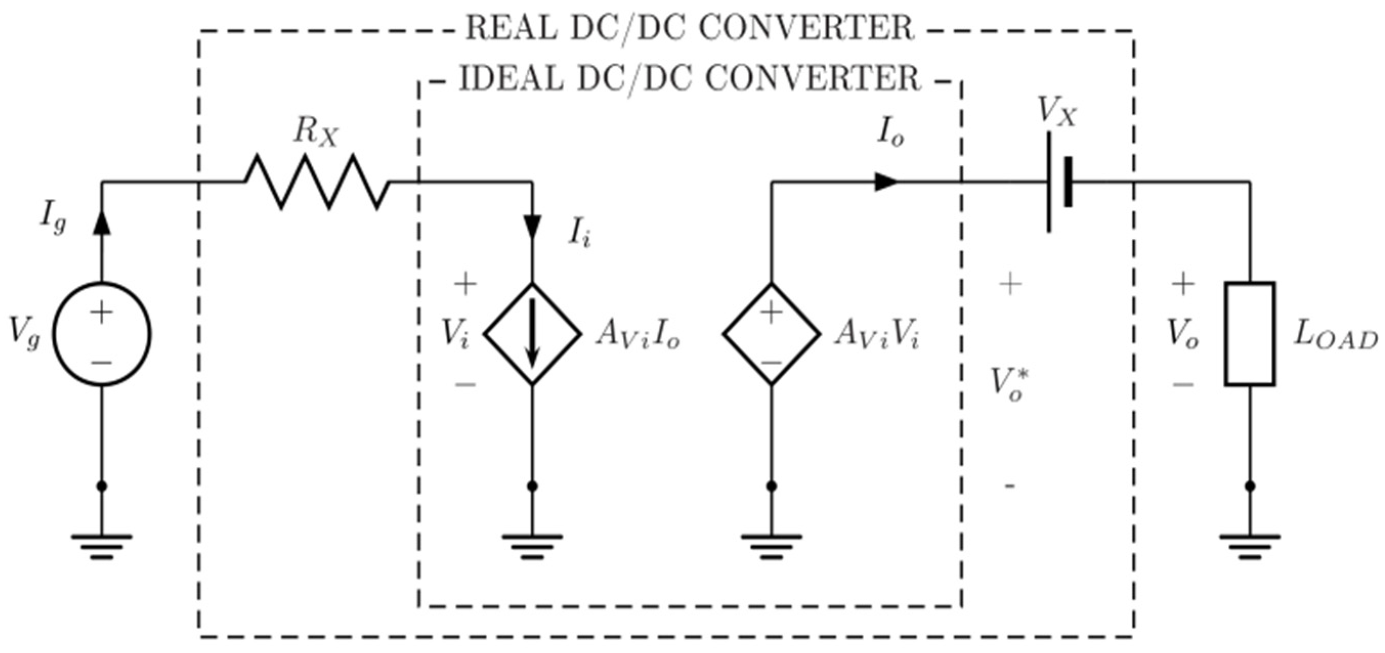
From here arises the challenge in finding a truly useful model, which provides close-to-experimentation results. It should also be simple, intuitive, easy to use and really general (i.e., valid for the three basic converter types: boost, buck and buck-boost). Figure 1 shows the proposed model, which is remarkably simple, as it comprises an ideal DC/DC converter formed by two voltage gain (AVi)-dependent sources: a current source in its input and a voltage source in its output. At the ideal converter input is connected an equivalent circuit consisting of the generator (Vg) and a series resistor (RX), which is aimed at concentrating all the losses of interest in the actual converter originated by the parasitic resistances of its components (active and passive). Of course, RX can be added to the generator internal resistance.
At the ideal converter output, a source (VX) and the load are connected. VX concentrates the losses in the actual converter due to the threshold voltage of its diode. Currents and voltages in the model are given by their mean values.
In this paper, and according to the model shown in Figure 1, the values of RX, VX and AVi are calculated for each basic topology (i.e., boost, buck and buck-boost). From here, input resistance, voltage gain and actual efficiency for each of these three topologies are found. Finally, model quality is assessed.
The present paper is structured as follows: Section 2 is devoted to setting the conditions for the developed model and its parameters. The parameter values for each basic topology are calculated in Section 3, Section 4 and Section 5: boost, buck and buck-boost respectively. Section 6 is devoted to comparing the results of the developed model regarding actual converters. In Section 7 the results are discussed, the fruit of which becomes clear with the excellent behavior of the model, practically like an actual converter. Finally, the paper ends with some conclusions.
2. Operating Modes of a DC/DC Converter. Definition of Parameters
Next, in order to make the paper self-contained, the two operating modes (depending on current iL through its inductor) of every DC/DC converter regardless of its topology are explained briefly. In addition, some parameters of interest will also be defined. The operating modes are:
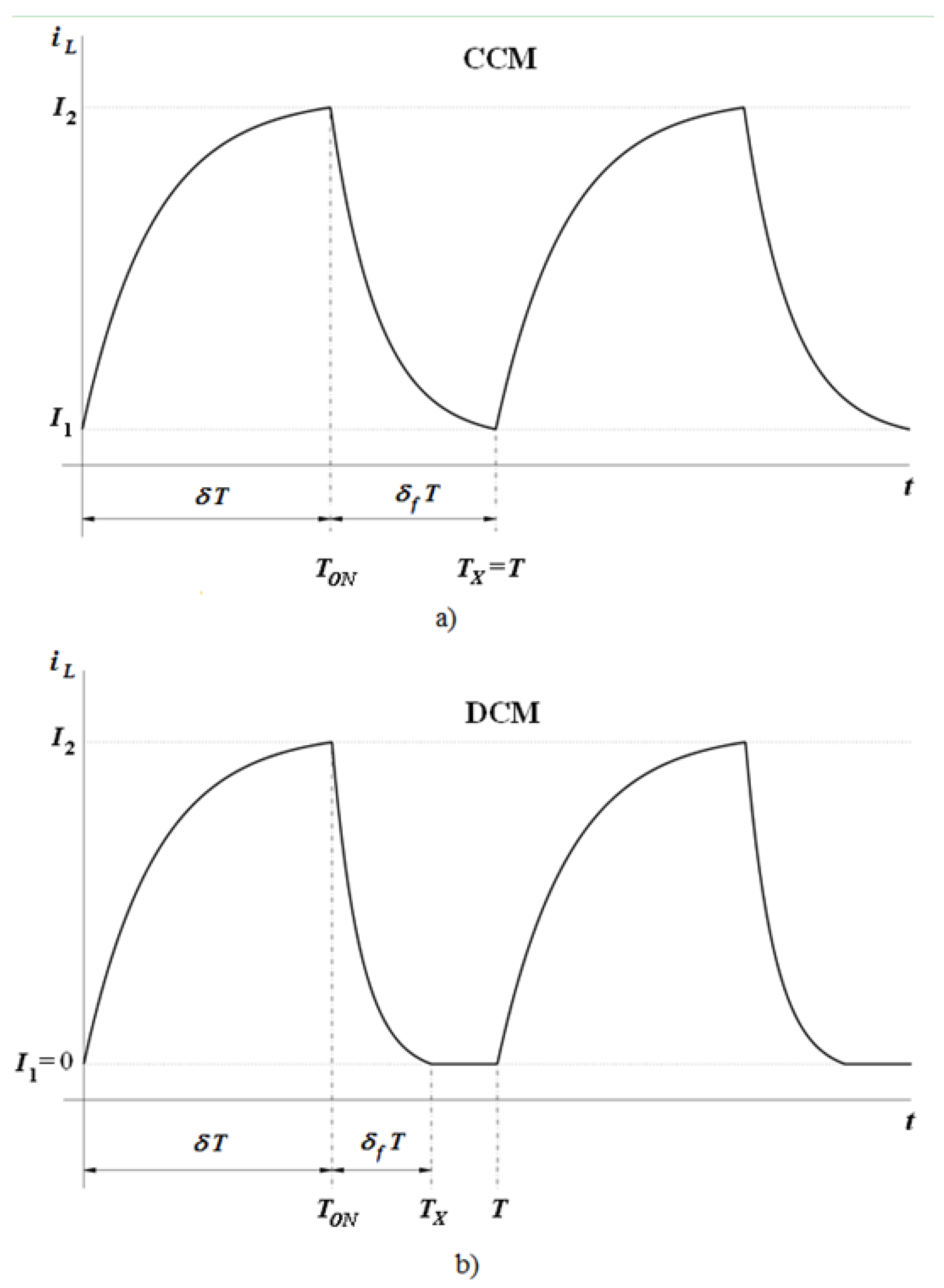
Continuous conduction mode (CCM): current always flows through the inductor (see Figure 2a).
Discontinuous conduction mode (DCM): current flows at controlled intervals through the inductor (see Figure 2b).
Note in Figure 2 that the current through the converter inductor is periodical with period T. This current in turn depends on the current supplied by the generator connected to the converter. The following parameters are defined (see Figure 1, Figure 2 and Figure 3).
However, in DCM, TX < T, so:
In the following study, with the aim of making currents and voltages independent from time, these will be characterized according to their mean value (indicated by a capital letter). Thus, for Ig (Figure 1 and Figure 2) during a switching period:
Both in CCM and DCM the third summing of (11) is null (Figure 2). Finally, the following hypothesis will be assumed: converters always operate in steady state regime (constant input voltage and fixed duty cycle according its operating conditions), the capacitor value C is to be assumed large enough and its losses negligible (very low equivalent series resistance, ESR). This allows consideration of a practically constant output voltage (Figure 3).
3. Boost Converter
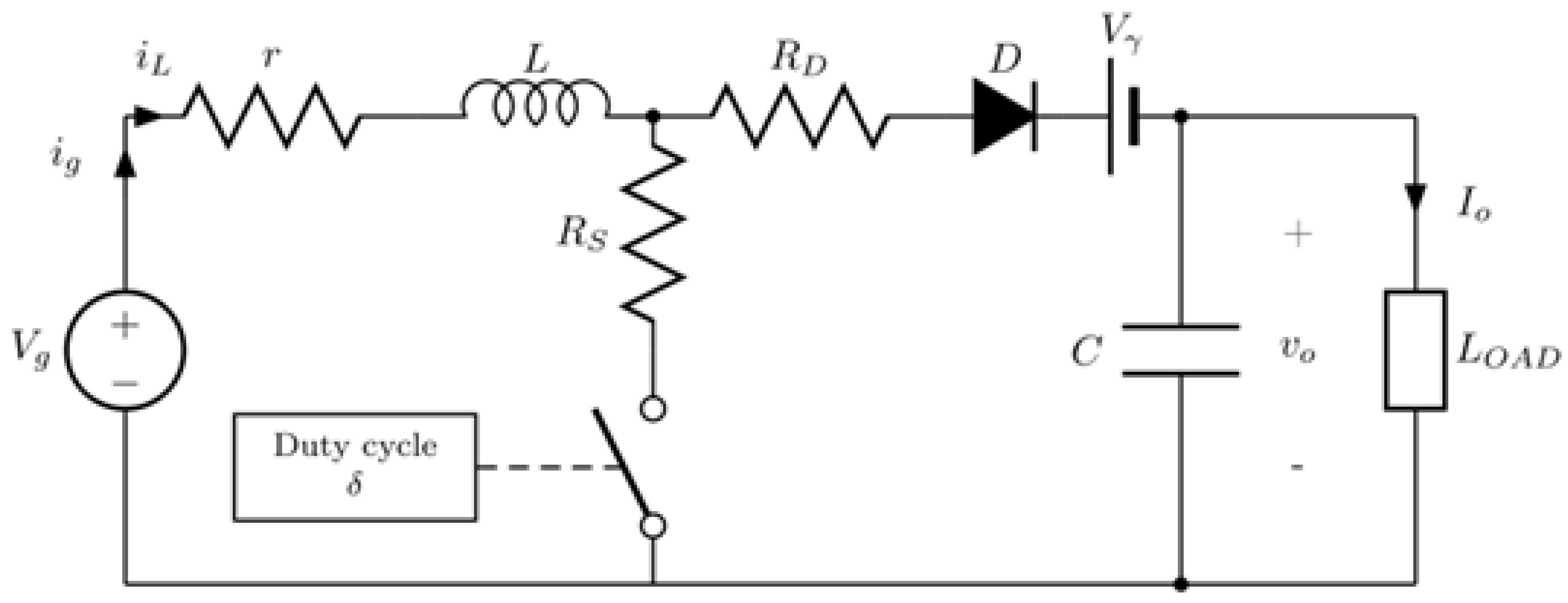
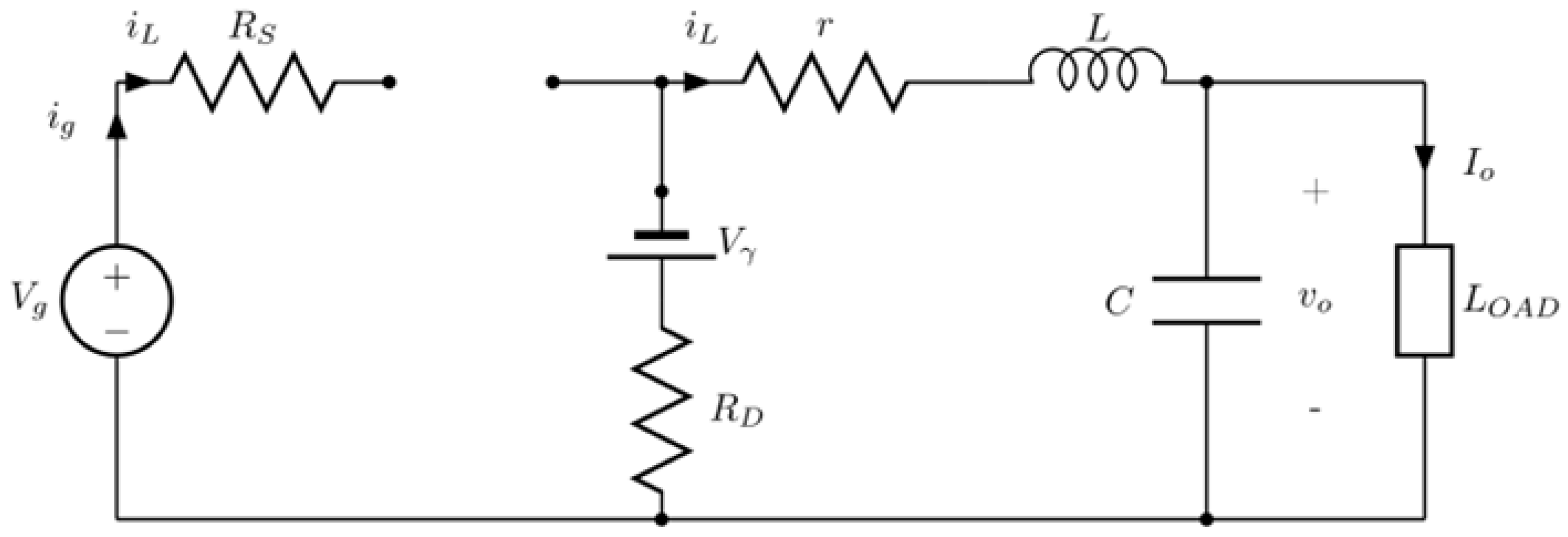
Figure 3 shows a boost converter that includes its main non-idealities (losses). Thus, r stands for the internal inductor resistance and RS for the power switch resistance in “on” state (closed). The leakage resistance of the power switch in “off” state (open) is so large that it can be considered an open circuit. RD is the forward (on) resistance of the freewheeling diode (the leakage resistance in off condition is so large that it can be considered an open circuit) and Vγ is its threshold voltage. The capacitor is considered an ideal element, as its series resistance has a very low value and its leakage resistance is very large (for capacitors of certain quality) whereby it can be neglected in parallel with the load.
3.1. Determination of the Generator-Supplied Current
In Figure 3, the mean current supplied by the generator within a given time period T (see Figure 2 and (11)) is:
Next we will analyze the behavior of the converter in the time intervals considered in (12).
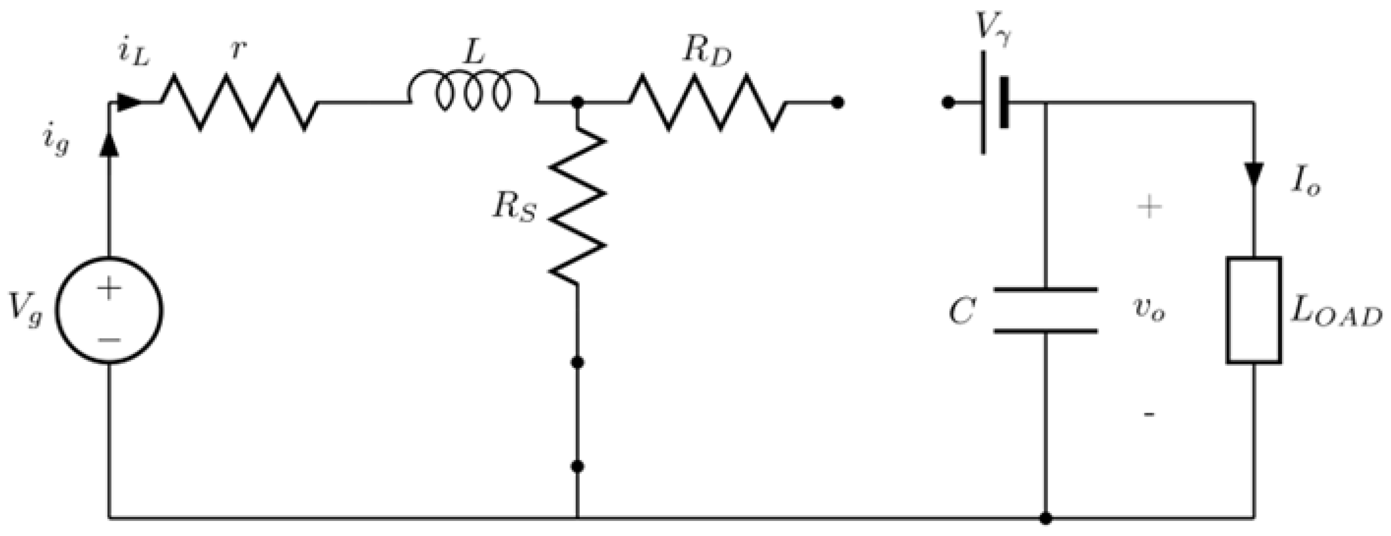
0 ≤ t ≤ TON
In this time interval, current through the inductor grows, the diode is reverse biased and therefore its branch is disconnected. Figure 4 shows the equivalent circuit.
From Figure 4 the following is deduced:
Solving it for iL and integrating the result into (12):
where and ΔI are given by (3) and (6) respectively. On the other hand, from (13), (4) and Figure 2 it follows that:
By a simple variable change in the left-hand integral:
where
and
Finally, by solving (16) for I1:
TON ≤ t ≤ TX
In this time interval, the diode branch is connected to the generator. Figure 5 shows the equivalent circuit. Figure 2a shows how current through the inductor drops exponentially (up to t = TX) in this time interval. At this point, if the current reaches 0 (DCM), it then keeps this value until new switch conduction (see Figure 2b).
From Figure 5 the following is deduced:
By solving it for iL and integrating the result into (12):
where is given by (5). On the other hand, from (20) and Figure 2 it follows that:
Now, by solving (22) as (15):
where
and
Finally, by solving (23) for I2:
The complete solution of (12) can be found by adding (14) and (21). However, both depend on ΔI, so this value must be calculated previously. For this, the equation system comprising (19), (26) and (6) is suggested:
By solving (27c) for I1 and substituting it in (27a):
An analogous procedure in (27c) and (27b) leads to:
Subtracting (29) from (28) and operating:
Now, multiplying the numerator and denominator in the left-side of (30) by and solving for ΔI:
where
Now (12) can be solved. Thus, from (14) and (21):
Substituting in this equation coefficients k1 and k2 given by (18) and (25) respectively:
where
Substituting now (31) in (34), the following is obtained:
Finally, substituting in the previous equation by its value in (8), it is finally obtained that:
3.2. Loss Resistance, Loss Voltage and Voltage Gain Determination
Of course, (38) and (39) show that in an ideal converter , so the efficiency is 1. At the input of the actual converter (Figure 1):
Multiplying the previous equation by and considering the load resistance connected to the converter,
From here the output voltage Vo is given by
where AVr is the converter actual voltage gain. That is:
At this point, we are interested in identifying the parameters RX, VX and AVi of the model of Figure 1. From it:
The previous equation is then compared to (37) to determine that:
and
Equations (45)–(47), respectively, allow obtaining the practical values (from Vγ, RD and RS given by the manufacturers of the converter components) of the model parameters (Figure 1) of a generic and real boost converter.
3.3. Input Resistance
This parameter is very important when the purpose of the converter is to match the generator output and load resistances. This is a typical application to achieve maximum power transfer from the generator to load. Then, from Figure 1, (40) and considering the load RL,
Now, by solving for Ri,
where RX, VX and AVi are given by (45)–(47) respectively. Equation (50) can be approximated taking into account that usually , wherewith,
3.4. Efficiency
Efficiency η is defined as the power ratio in the load and that supplied by the generator (Figure 1):
Now, substituting AVr by its value given in (43):
where RX, VX and AVi are given by (45)–(47) respectively.
3.5. Conventional Approximate Analysis
It is interesting to show how from the exact expressions of RX and AVi, (45) and (47) respectively, it is easy to get their common idealized CCM values [24,36,37,38,39]:
and
Let us assume that at the working frequency (see (17) and (24)). Under this premise, and . Substituting these values in (32):
Keep in mind that being , . On the other hand, according to (18), (25), and (35):
It is rather common that which leads to . Thus, . Them from (45):
Usually and , so (58) can be written as:
From (47) and taking into account again that and AVi can be approximated to:
In CCM , wherewith (59) and (60) lead to (54) and (55) respectively, which are the usual simplifications in the literature.
Analogously from (51) and with (59) and (60) in CCM,
Finally, from (53), (46) and with (59) and (60) in CCM,
3.6. Discontinuous Conduction Mode (DCM)
In DCM (see Figure 2b), (27) will be written as:
By solving (63a) for I2 and substituting the result in (63b),
From given by (24), it is easy to get the duty cycle value that sets the boundary between DCM and CCM:
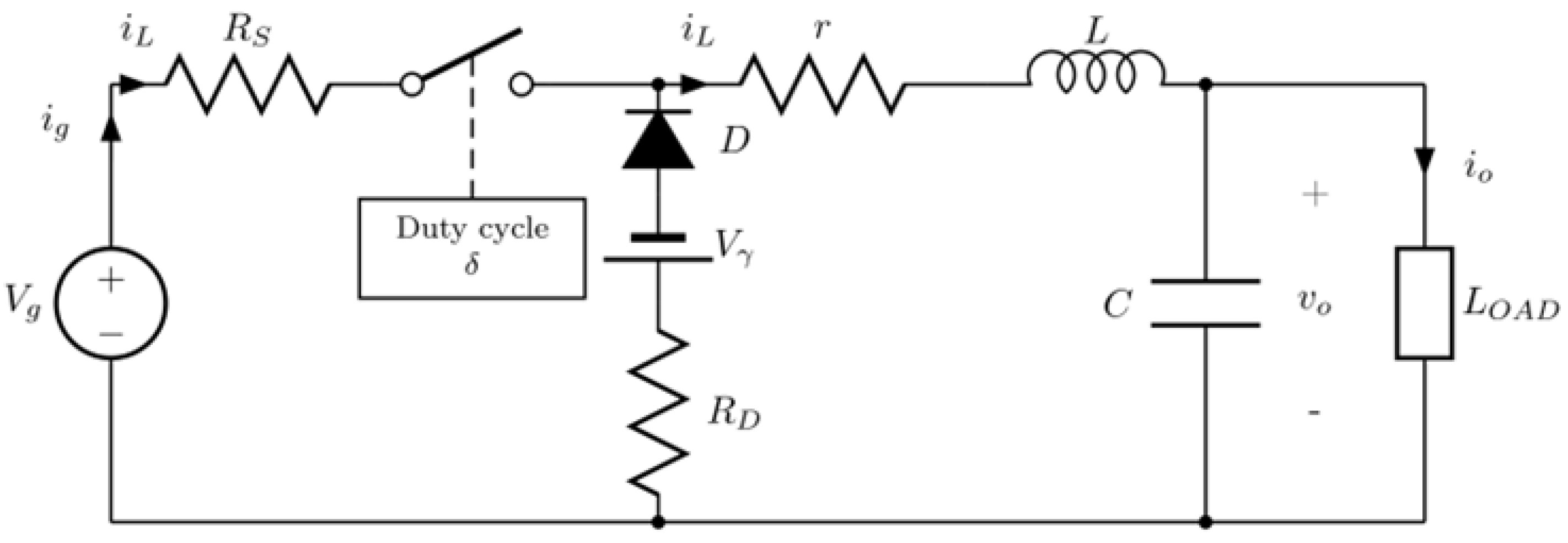
4. Buck Converter
Figure 7 shows a buck converter with its main non-idealities.
4.1. Determination of Generator-Supplied Current
We are going to analyze the behavior of the converter in the time intervals considered in (11). Now, in both operation modes, the mean current supplied by the generator within a given time period T (see Figure 2 and (11)) is
A similar analysis to Section 3 will then be carried out.
0 ≤ t ≤ TON
In this time interval current through the inductor grows, the diode is reversing biased and its branch is disconnected. Figure 8 shows the equivalent circuit.
Reasoning in Figure 8 like from (13) to (14), but now for ,
Now, operating like from (15) to (19) it comes to
TON ≤ t ≤ TX
Now the generator branch is disconnected. Figure 9 shows the equivalent circuit.
Reasoning on Figure 9 like from (20) to (21),
Now, operating like from (22) to (26),
At this point, as in the step to (27), the equation system formed by (68), (70), and (6) is suggested:
Solving (71) in the same way that from (27) to (31):
with β given in (32).
Now we can calculate the current supplied by the generator in the interval that “sees” the load. Therefore, substituting (72) into (67),
Taking into account k1 and k2 values from (18) and (25) respectively, ΔV from (7) and considering (35),
4.2. Loss Resistance, Loss Voltage and Voltage Gain Determination
With the aim of identifying RX, VX and AVi according to the converter parameters given in Figure 1, we proceeded as follows. Comparing (44) and (74) the following is obtained:
and
Substituting (75)–(77) in (43), it is immediate to calculate the converter actual voltage gain, Avr.
4.3. Input Resistance
It is immediate, simply replace RX, VX and AVi from (75)–(77), respectively, in (50).
4.4. Efficiency
Again it is immediate, simply replace RX, VX and AVi from (75) to (77), respectively, in (53).
4.5. Conventional Approximate Analysis
Assume that at the working frequency, β can be approximated like in (56), whereby
As in Section 3.5 (reasoning after (57)), under the commonest operating conditions and you have to
Then, (75) and (77) can be approximated respectively to:
and
Finally, regarding (76), considering in this order: (25), (56) with (17) and (24), and (35) with (18), it can be rewritten as:
If the converter works in CCM (82) and (83) lead to the literature common expressions [24,36,37,38,39]:
and
On the other hand, substituting (82) and (83) in (51):
that for CCM condition leads to:
Similarly, (84) can be written in CCM as:
Regarding approximate efficiency determination, it is enough to substitute (82)–(84) in (53) with the condition that :
This efficiency for CCM condition can be written as:
4.6. Discontinuous Conduction Mode (DCM)
For this mode, (71) is expressed as follows:
By solving (92a) for I2 and substituting the result in (92b),
Finally, from value given by (24), the duty cycle value that sets the boundary between DCM and CCM can be calculated from (93) as
where k1 and k2 are given by (18) and (25) respectively.
5. Buck-Boost Converter
Figure 10 shows a buck-boost converter that includes its main non-idealities (losses).
5.1. Determination of Generator-Supplied Current
In Figure 10, the mean current supplied by the generator within a given time period T (see Figure 2 and (11)) is:
Next we will proceed like in the previous sections.
0 ≤ t ≤ TON
In this time interval the diode branch is disconnected. Figure 11 shows the equivalent circuit.
Equation (96) is analogous to (14), wherewith and as might be expected, (97) is also (19):
TON ≤ t ≤ TX
Now the generator branch is disconnected. Figure 12 shows the equivalent circuit.
Reasoning on Figure 12 like from (20) to (21),
Now, operating like from (22) to (26),
As we did in (27), It is now suggests the equation system comprising (97), (99) and (6):
By solving (100) in the same way that from (27) to (31):
with β given in (32).
Now we can calculate the current supplied by the generator. So substituting (101) into (96),
Taking into account k1 and k2 values from (18) and (25) respectively,
5.2. Loss Resistance, Loss Voltage and Voltage Gain Determination
With the aim of identifying RX, VX and AVi according to the converter parameters given in Figure 1, we are going to proceed as follows. Comparing (44) and (103), the following is obtained:
and
5.3. Input Resistance
Substituting RX, VX and AVi from (104)–(106), respectively, in (50):
5.4. Efficiency
Substituting RX, VX and AVi from (104)–(106), respectively, in (53):
5.5. Conventional Approximate Analysis
Assume that at the working frequency β is (56), so is (81). This allows writing (104) as
Again, taking into account in (106) that is (81) and the fact that
If the converter works in CCM (109) and (110) leads to the common expressions in literature [24,36,37,38,39]:
and
On the other hand, substituting (111) and (112) in (50):
that for CCM condition can be written as
Regarding approximate efficiency determination, it is enough to substitute (105), (109) and (110) in (53) with the condition that :
that for CCM is expressed as follows:
5.6. Discontinuous Conduction Mode (DCM)
For this mode, (100) can be written as follows:
By solving (117a) for I2 and substituting the result in (117b),
Matching this result with (24) and taking into account (25), the duty cycle value that sets the boundary between DCM and CCM is
6. Results
Now we are going to show the suitability of the developments carried out. For that, the results obtained by the theoretical study (developed model) are going to be compared with the results obtained by actual converters. In order to have a broader perspective and it be able to show in a clear way the quality of the developed model, it will be also included in the comparison with the results by the conventional model used in the literature [24,36,37,38,39]. Note, see for example (61) or (62), that the conventional model only considers a non-ideality (losses), specifically the internal inductor resistance r.
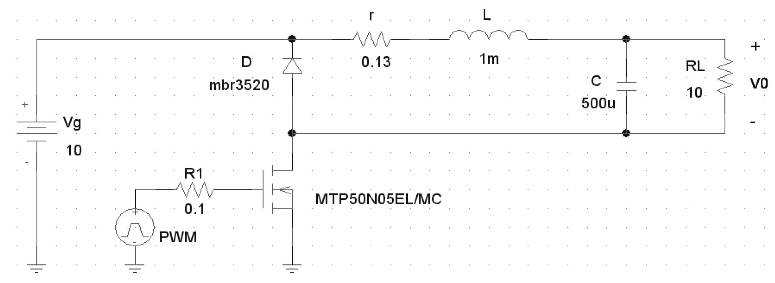
Figure 13, Figure 14 and Figure 15 show the PSpice simulation circuits for the three DC/DC power converters’ basic topologies analyzed. For simulations we have used commercial diodes and switches. This allows working with actual values of Vγ, RD and RS. Regarding r, it has been obtained by measuring a 1 mH inductor made in the laboratory. For example, 10 V has been chosen for Vg and 20 or 10 Ω (depending on the characteristics of the active components) for RL. Finally, we have used f = 10 kHz because it is usual in DC/DC power converters.
6.1. Boost Converter
Figure 16 shows the model-predicted AVr (introducing (45)–(47), with their respective values, into (43)) and the actual obtained by simulation (by the circuit of Figure 13).
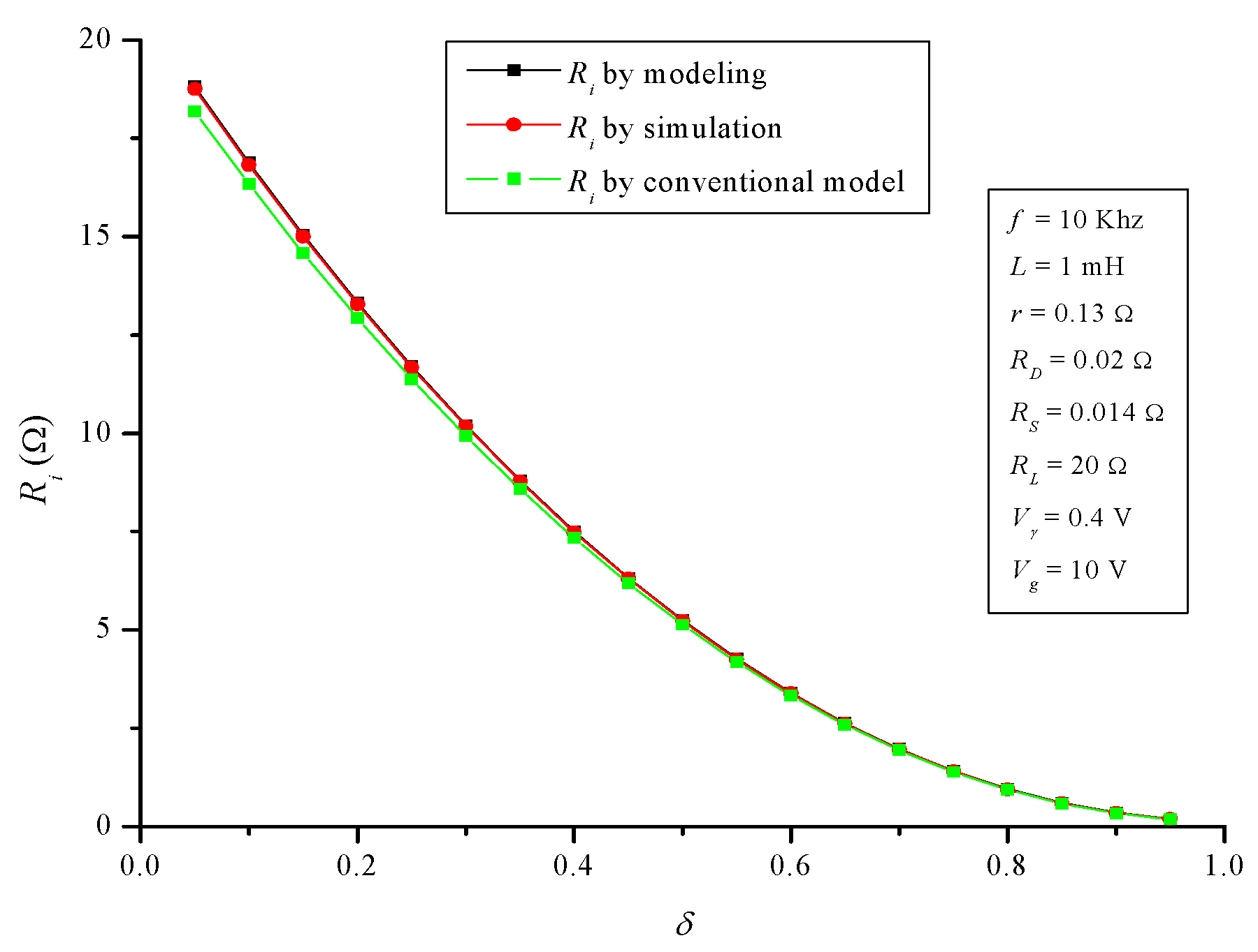
Regarding input resistance, Figure 17 shows the model-predicted (introducing (45)–(47), with their respective values, into (50)), and by simulation.
Finally, regarding efficiency, Figure 18 shows model-predicted (introducing (45)–(47), with their respective values, into (53)), and by simulation.
6.2. Buck Converter
6.3. Buck-Boost Converter
From the results shown in Figure 16, Figure 17, Figure 18, Figure 19, Figure 20, Figure 21, Figure 22, Figure 23 and Figure 24, Table 1 summarizes the normalized mean absolute percent error (NMAE%) for the developed and conventional models regarding the actual converters.
Finally, Table 2 summarizes the obtained parameters of the developed model.
7. Discussion
Now we are going to discuss the results of the previous section and of the whole paper in general. As we are going to demonstrate next, the quality of the developed model (Figure 1) is excellent for the three DC/DC power converters’ basic topologies.
First of all it is important to discuss the way to obtain in the literature [24,36,37,38,39] the conventional expressions (practically ideal, h = 1, except for taking into account the internal inductor resistance r) for AVr, Ri and h. Authors arrive at these expressions from approximations from the beginning, specifically considering that the current through r is constant and equal to a mean value. In the developed model, you get to the same expressions (Section 3.5, Section 4.5 and Section 5.5), but without previous approximations and by the resolving of exact equations.
Analyzing Figure 16 it is easy to note how the developed model fits the voltage gain (AVr) of the actual boost converter. In fact, as you can see in Table 1, the (NMAE%) is negligible, only 0.45%. Figure 16 shows up the great influence of its non-idealities on an actual boost converter operation. Ideally, a boost converter presents no upper limit in the gain (55), so it can take anyone above 1. However, in the actual case, as it is well known, and the developed model is able to show, the gain is drastically modified. Although the conventional model error is also small (2.93%), it is 6.5 times greater than the developed model.
Continuing the boost converter and regarding its input resistance, Figure 17 shows again the quality of the model, NMAE% is very small, only 0,66% (2.19% in the conventional model). Finally, regarding efficiency, Figure 18 shows that NMAE is again negligible, 0.3%. Here is where the difference among the quality of the developed model and the conventional one is more notable, specifically the error of the latter is 9 times greater (2.69%). Knowing the actual efficiency of a converter is very important; in fact, in most facilities, DC/DC converters are a post-generator mandatory stage. The foregoing means that the overall efficiency of the system up to the regulated-voltage output is the product of the generator and converter efficiency. Thus, it is of great interest to know the actual DC/DC converter losses and, from them, its true efficiency.
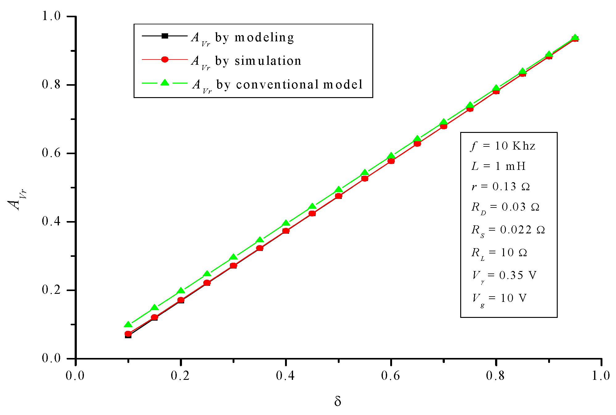
Now, regarding the buck converter, Figure 19, Figure 20 and Figure 21 show the behavior of AVr, Ri and η. For the developed model, NMAE% is again negligible: 0.73%, 1.61% and 0.31% respectively. However, for the conventional model, NMAE% is 7.10%, 5.39% and 8.09% respectively. Again the differences are notable, and especially regarding efficiency, where the error is much worse than in the buck converter, specifically 26 times greater.
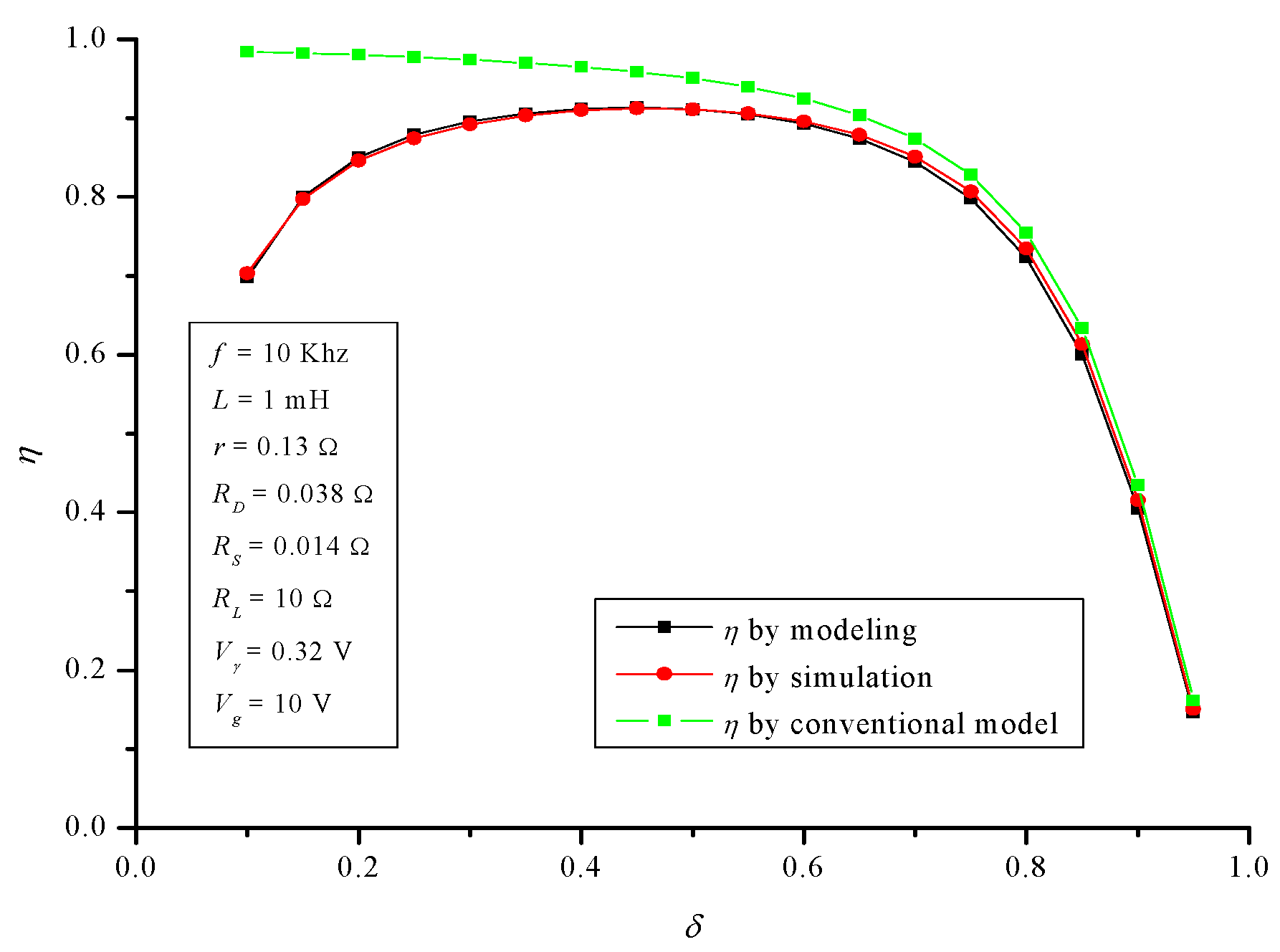
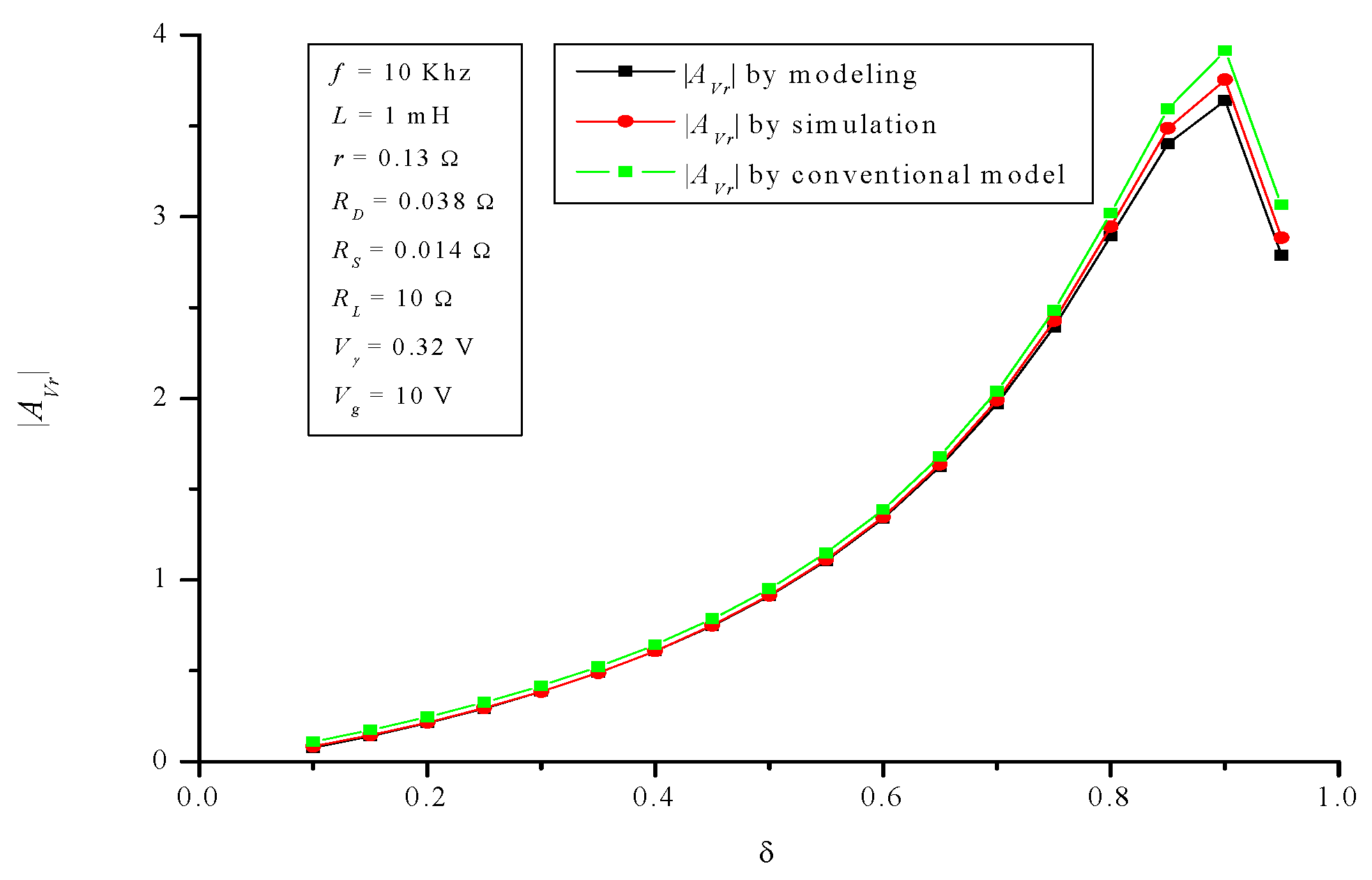
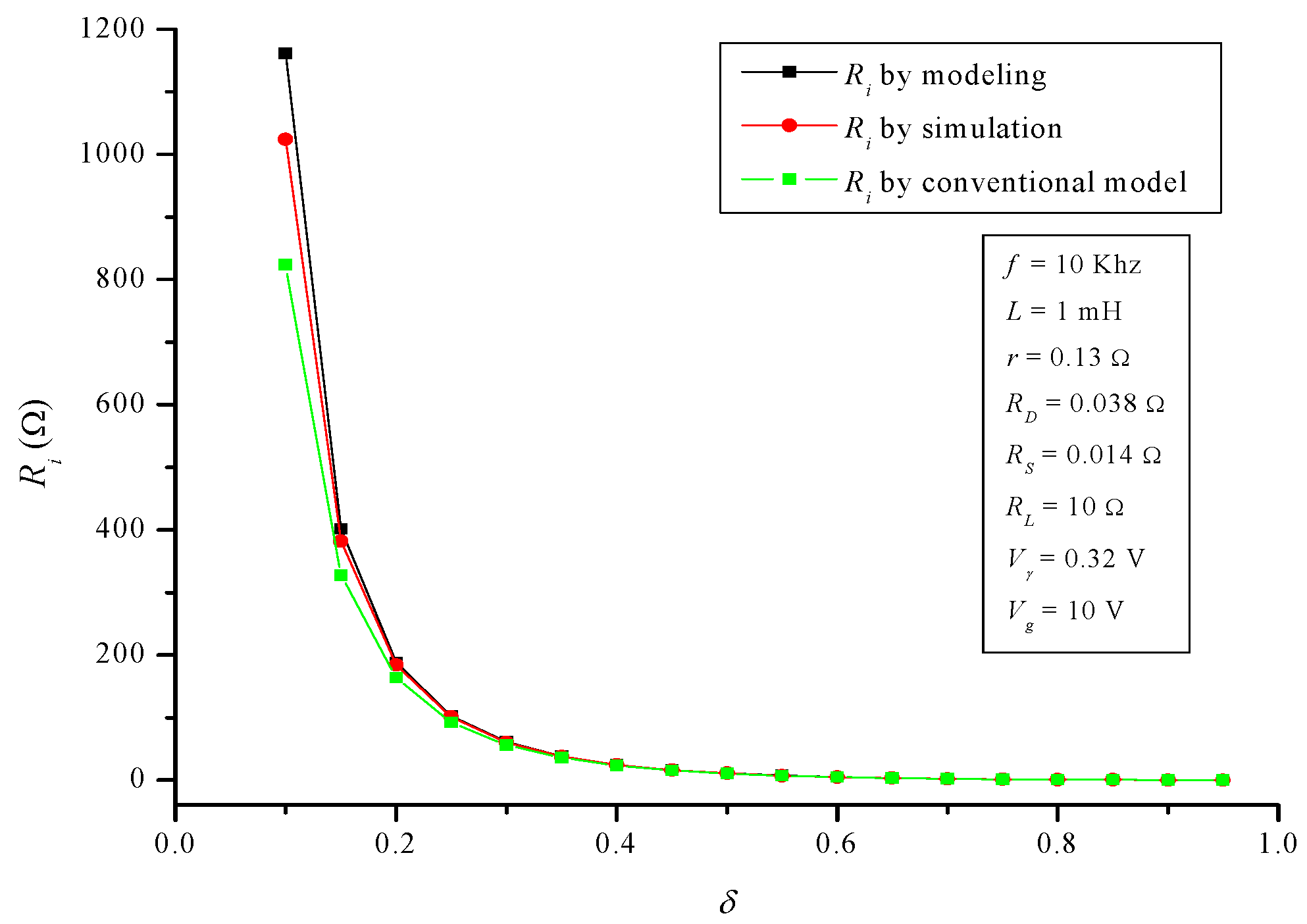
Finally, regarding buck-boost converter, Figure 22, Figure 23 and Figure 24 show the behavior of AVr, Ri and η. For the developed model, NMAE% is once again negligible: 1.4%, 1.98% and 0.84% respectively. In the case of the conventional model, NMAE% is: 7.57%, 5.87% and 8.65% respectively. Now, the efficiency error is more than 10 times greater in the conventional model regarding the developed one.
Going back to Section 3.5, Section 4.5 and Section 5.5 that attend to the idealizations, it is important to point out that in the converter literature, and also in converter teaching, it is very common to work with idealized expressions, which are of common use for students, teachers and postgraduate engineers. The developed model shows how it is possible to go in an easy way from exact expressions to idealized ones.
Continuing with the above and in view of the development carried out in Section 3, Section 4 and Section 5 of this paper, it may seem that the complexity of the modeling method may be quite high. However, in the opinion of the authors, this is not true for four reasons: (1) the approach is very intuitive; (2) the laws of circuit theory that have been applied are very simple and known; (3) the mathematical analysis used is within the scope of any student of engineering degree; and (4) the methodology and steps are identical for the three converter topologies. Moreover, one might think that for practical converters, the difference between the results of the accurate analysis carried out in this paper and the conventional approximate analysis is too small to justify the extra analytical effort (the results are shown in Table 1). Well, this can be true in some cases (especially in converters that work in a small range of their duty cycle), but not always, and in any case, the use of the developed model is very easy in practice, because it does not require any mathematical development. It is enough to apply directly to Figure 1 the parameter values that have been developed in the paper, depending on the converter, which has been summarized in Table 2. The parameter values can be obtained immediately from the data sheets of the converter components (no measurements are needed).
Finally, regarding the capacitor value C in the three topologies, it has been assumed to be large enough and with negligible losses (very low equivalent series resistance, ESR). This has allowed the consideration of a practically constant output voltage . The ESR is inversely proportional to the capacity and today, for typical capacities of C in power converters applications, it is easy to find capacitors with ESR < 0.010 Ω.
8. Conclusions
An intuitive approach to model the steady state regime of the three DC/DC power converters’ basic topologies (buck, boost and buck-boost) has been developed in this work. This approach is new because it is not present in the literature. Besides, the developed model is common (it is suitable for the three basic topologies), realistic (it includes the main non-idealities (losses) of the active and passive components of the three topologies), accurate (the behavior of the real converter and its model are very close) and practical (it demands no measurements and just needs to have the data provided by the manufacturers’ data sheets of the converter components).
The developed model transforms a complex system with strong non-idealities in the form of distributed parameters, into a simple and intuitive scheme of concentrated parameters, which accurately reflect the actual behavior of the converters components.
The quality of the developed model has been checked by two independent lines. The first has been to probe how the relationships developed in this work can lead to the approximations commonly used in literature. The second has demonstrated how the behavior of the developed model matches the behavior of an actual converter in any of the studied basic structures. Moreover, the developed model has been subjected to a battery of comparatives for the three types of basic converters regarding the conventional model used until now in the literature. The results are summarized in Table 1 and the conclusion can be that the quality of the developed model is excellent and it far exceeds the conventional model.
As a future work that in fact it is already running, authors of this manuscript are working to try to extend the approach presented in this paper to other DC/DC converters topologies.
Author Contributions
Juan Manuel Enrique and José Manuel Andújar conceived and designed the model; Eladio Durán performed the experiments; Antonio Javier Barragán analyzed and wrote the paper.
Conflicts of Interest
The authors declare no conflict of interest.
References
- Blaabjerg, F.; Chen, Z.; Kjær, S.B. Power electronics as efficient interface in dispersed power generation systems. IEEE Trans. Pow. Electron. 2004, 19, 1184–1194. [Google Scholar] [CrossRef]
- Ferrera, M.B.; Durán, E.; Pérez, S.; Andújar, J.M. A Converter for Bipolar DC Link Based on SEPIC-Cuk Combination. IEEE Trans. Pow. Electron. 2015, 30, 6483–6487. [Google Scholar] [CrossRef]
- Durán, E.; Galán, J.A.; Sidrach-de-Cardona, M.; Andújar, J.M. A new application of the buck-boost-derived converters to obtain the I-V curve of photovoltaic modules. In Proceedings of the Power Electronics Specialists Conference, Orlando, FL, USA, 17–21 June 2007; pp. 413–417. [Google Scholar] [CrossRef]
- Segura, F.; Andújar, J.M. Power management based on sliding control applied to fuel cell systems: A further step towards the hybrid control concept. Appl. Energy 2012, 99, 213–225. [Google Scholar] [CrossRef]
- Vasallo, M.J.; Andújar, J.M.; García, C.; Brey, J.J. A Methodology for Sizing Backup Fuel-Cell/Battery Hybrid Power Systems. IEEE Trans. Ind. Electron. 2010, 57, 1964–1975. [Google Scholar] [CrossRef]
- Segura, F.J.; Andújar, J.M.; Durán, E. Analog Current Control Techniques for Power Control in PEM Fuel Cell Hybrid Systems: A Critical Review and a Practical Application. IEEE Trans. Ind. Electron. 2011, 88, 1171–1184. [Google Scholar] [CrossRef]
- Chakraborty, C.; Iu, H.H.-C.; Lu, D.D.-C. Power Converters, Control, and Energy Management for Distributed Generation. IEEE Trans. Ind. Electron. 2015, 62, 4466–4470. [Google Scholar] [CrossRef]
- Andújar, J.M.; Segura, F.; Durán, E.; Rentería, L.A. Optimal interface based on power electronics in distributed generation systems for fuel cells. Renew. Energy 2011, 36, 2759–2770. [Google Scholar] [CrossRef]
- Segura, F.; Durán, E.; Andújar, J.M. Design, building and testing of a stand-alone fuel cell hybrid system. J. Power Sour. 2009, 193, 276–284. [Google Scholar] [CrossRef]
- Na, W.; Chen, P.; Kim, J. An Improvement of a Fuzzy Logic-Controlled Maximum Power Point Tracking Algorithm for Photovoltaic Applications. Appl. Sci. 2017, 7, 326. [Google Scholar] [CrossRef]
- Zhang, G.; Qian, J.; Zhang, X. Application of a High-Power Reversible Converter in a Hybrid Traction Power Supply System. Appl. Sci. 2017, 7, 282. [Google Scholar] [CrossRef]
- Chen, M.; Ma, S.; Wu, J.; Huang, L. Analysis of MPPT Failure and Development of an Augmented Nonlinear Controller for MPPT of Photovoltaic Systems under Partial Shading Conditions. Appl. Sci. 2017, 7, 95. [Google Scholar] [CrossRef]
- Valera-García, J.J.; Atutxa-Lekue, I. Integrated Power Systems for Offshore Vessels. Control, trends and challenges. Rev. Iberoam. Autom. Inf. Ind. 2016, 13, 3–14. [Google Scholar] [CrossRef]
- Piris-Botalla, L.; Oggier, G.G.; Airabella, A.M.; García, G.O. Extending the sot-switching operating range of a bidirectional three-port DC-DC converter. Rev. Iberoam. Autom. Inf. Ind. 2016, 13, 127–134. [Google Scholar] [CrossRef]
- Real-Calvo, R.; Moreno-Munoz, A.; Pallares-Lopez, V.; Gonzalez-Redondo, M.J.; Moreno-Garcia, I.M.; Palacios-Garcia, E.J. Intelligent Electronic System to Control the Interconnection Between Distributed Generation Resources and Power Grid. Rev. Iberoam. Autom. Inf. Ind. 2017, 14, 56–69. [Google Scholar] [CrossRef]
- Middlebrook, R.D.; Cuk, S. Modeling and analysis methods for DC-to-DC switching converters. In Proceedings of the IEEE International Semiconductor Power Converter Conference, Lake Buena Vista, FL, USA, 28–31 March 1977; pp. 90–111. [Google Scholar]
- Wester, G.W. Low-Frequency Characterization of Switched DC-DC Converters. Ph.D. Thesis, California Institute of Technology, Pasadena, CA, USA, 1972. [Google Scholar]
- Wester, G.W.; Middlebrook, R.D. Low-frequency characterization of switched DC-to-DC converters. IEEE Trans. Aeros. Electron. Syst. 1973, AES-9, 376–385. [Google Scholar] [CrossRef]
- Owen, H.A.; Capel, A.; Ferrante, J.G. Simulation and analysis methods for sampled power electronic systems. In Proceedings of the IEEE Power Electronics Specialists Conference, Cleveland, OH, USA, 8–10 June 1976; pp. 45–55. [Google Scholar] [CrossRef]
- Lee, F.C.Y.; Iwens, R.P.; Yu, Y.; Triner, J.E. Generalized computer-aided discrete time domain modeling and analysis of DC-DC converters. IEEE Trans. Ind. Electron. Cont. Inst. 1979, IECI-26, 58–69. [Google Scholar] [CrossRef]
- Cuk, S.; Middlebrook, R.D. A general unified approach to modelling switching dc-to-dc converters in discontinuous conduction mode. In Proceedings of the IEEE Power Electronics Specialists Conference, Palo Alto, CA, USA, 14–16 June 1977. [Google Scholar] [CrossRef]
- Vorperian, V.; Cuk, S. Small signal analysis of resonant converters. In Proceedings of the IEEE Power Electronics Specialists Conference, Albuquerque, NM, USA, 6–9 June 1983. [Google Scholar] [CrossRef]
- Vorperian, V.; Tymerski, R.; Lee, F.C.Y. Equivalent circuit models for resonant and PWM switches. IEEE Trans. Power Electron. 1989, 4, 205–214. [Google Scholar] [CrossRef]
- Vorperian, V. Simplified analysis of PWM converters using model of PWM switch. Part I and II. IEEE Trans. Aeros. Electron. Syst. 1990, 26, 490–505. [Google Scholar] [CrossRef]
- Sanders, S.R.; Noworolski, J.M.; Liu, X.Z.; Verghese, G.C. Generalized averaging method for power conversion circuits. IEEE Trans. Power Electron. 1991, 6, 251–259. [Google Scholar] [CrossRef]
- Noworolski, J.M.; Sanders, S.R. Generalized in-plane circuit averaging. In Proceedings of the IEEE Applied Power Electronics Conference and Exposition, Dallas, TX, USA, 10–15 March 1991. [Google Scholar] [CrossRef]
- Oliver, J.A.; Cobos, J.A.; Uceda, J.; Rascon, M.; Quinones, C. Systematic approach for developing large-signal averaged models of multi-output PWM converters. In Proceedings of the IEEE Power Electronics Specialists Conference, Galway, Ireland, 23 June 2000. [Google Scholar] [CrossRef]
- Luowei, Z.; Sucheng, L.; Weiguo, L.; Shuchang, H. Quasi-steady-state large-signal modelling of DC-DC switching converter: Justification and application for varying operating conditions. IET Power Electron. 2014, 7, 2455–2464. [Google Scholar] [CrossRef]
- Yan, Y.; Lee, F.C.; Mattavelli, P. Comparison of small signal characteristics in current mode control schemes for point-of-load buck converter applications. IEEE Trans. Power Electron. 2013, 28, 3405–3414. [Google Scholar] [CrossRef]
- Xin, L.; Xinbo, R.; Qian, J.; Mengke, S.; Chi, K.T. Small-Signal Models with Extended Frequency Range for DC-DC Converters with Large Modulation Ripple Amplitude. IEEE Trans. Power Electron. 2017. [Google Scholar] [CrossRef]
- El Aroudi, A.; Giaouris, D.; Iu, H.H.-C.; Hiskens, I.A. A review on stability analysis methods for switching mode power converters. IEEE J. Emerg. Sel. Top. Circuits Syst. 2015, 5, 302–315. [Google Scholar] [CrossRef]
- Zhioua, M.; El Aroudi, A.; Belghith, S.; Bosque-Moncusí, J.M.; Giral, R.; Al Hosani, K.; Al-Numay, M. Modeling Dynamics Bifurcation Behavior and Stability Analysis of a DC-DC Boost Converter in Photovoltaic Systems. Int. J. Bifur. Chaos 2016, 26, 1650166. [Google Scholar] [CrossRef]
- Beg, O.A.; Abbas, H.; Johnson, T.T.; Davoudi, A. Model Validation of PWM DC-DC Converters. IEEE Trans. Ind. Electron. 2017, 64, 7049–7059. [Google Scholar] [CrossRef]
- Enrique, J.M.; Durán, E.; Sidrach-De-Cardona, M.; Andújar, J.M. Theoretical Assessment of the Maximum Power Point Tracking Efficiency of Photovoltaic Facilities with Different Converter Topologies. Sol. Energy 2007, 81, 31–38. [Google Scholar] [CrossRef]
- Durán, E.; Andújar, J.M.; Galán, J.A.; Sidrach-De-Cardona, M. Methodology and experimental system for measuring and displaying I-V characteristic curves of PV facilities. Prog. Photovoltaic. Res. Appl. 2009, 17, 574–586. [Google Scholar] [CrossRef]
- Erickson, R.W.; Cuk, S.; Middlebrook, R.D. Large-signal modelling and analysis of switching regulators. In Proceedings of the IEEE Power Electronics Specialists Conference, Cambridge, MA, USA, 14–17 June 1982. [Google Scholar] [CrossRef]
- Middlebrook, R.D.; Cuk, S. A General Unified Approach to Modelling Switching-Converter Power Stages. In Proceedings of the IEEE Power Electronics Specialists Conference, Cleveland, OH, USA, 8–10 June 1976. [Google Scholar] [CrossRef]
- Singer, S.; Erickson, R. Canonical modeling of power processing circuits based on the POPI concept. IEEE Trans. Power Electron. 1992, 7, 37–43. [Google Scholar] [CrossRef]
- Tamerski, R.; Vorperian, V. Generation, Classification and Analysis of Switched-Mode DC-to-DC Converters by the Use of Converter Cells. In Proceedings of the Elecommunications Energy Conference, Toronto, ON, Canada, 19–22 October 1986. [Google Scholar] [CrossRef]
Figure 1.
Common static model for DC/DC power converters basic topologies.

Figure 2.
Current iL through the inductor of the DC/DC converter: (a) CCM and (b) DCM.

Figure 3.
Boost converter circuit including its main non-idealities (losses).

Figure 4.
Equivalent boost converter circuit for 0 ≤ t ≤ TON.

Figure 5.
Equivalent boost converter circuit for TON ≤ t ≤ TX.
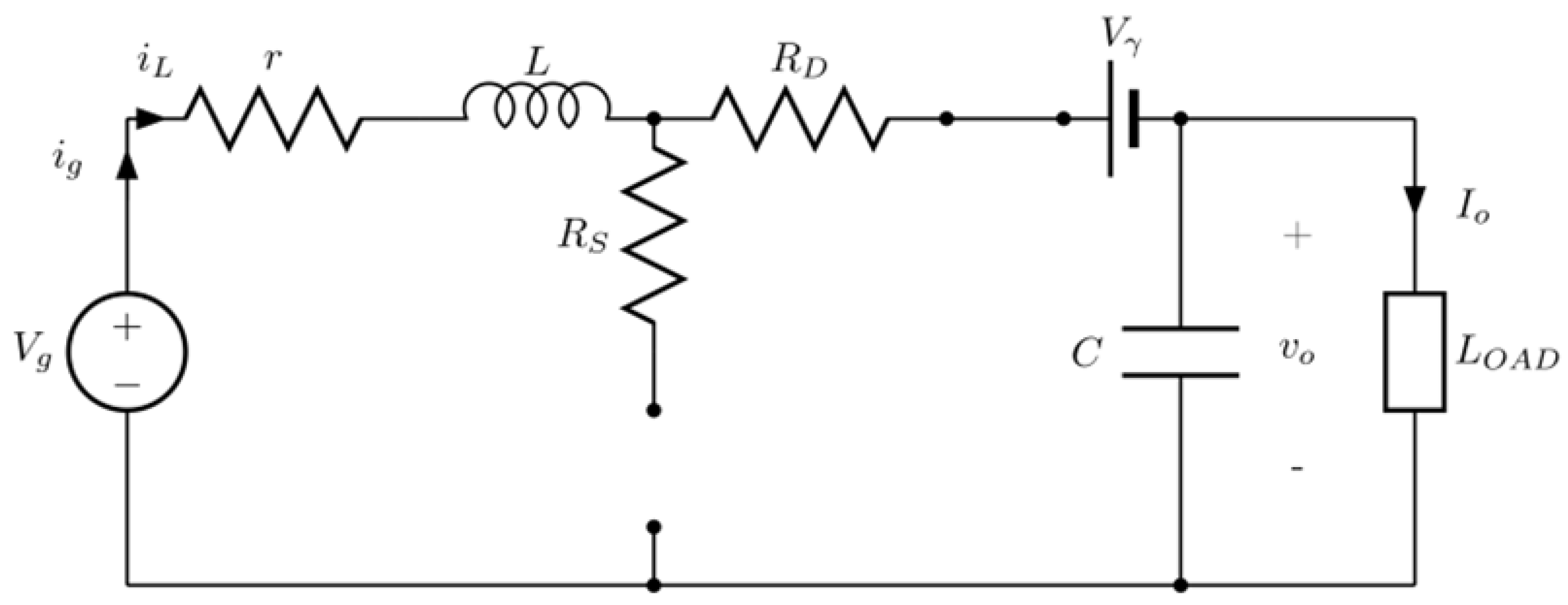
Figure 6.
Total loss resistance RX for the boost converter.
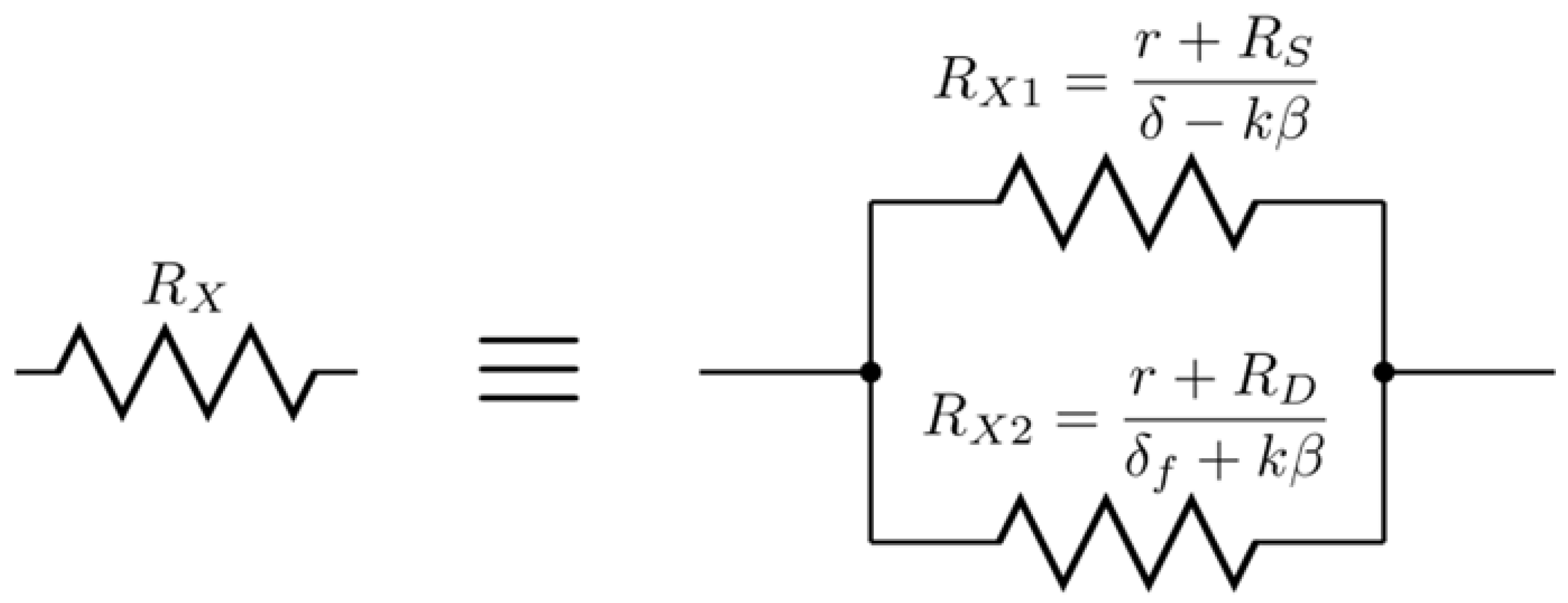
Figure 7.
Buck converter circuit including its main non-idealities (losses).

Figure 8.
Equivalent buck converter circuit for 0 ≤ t ≤ TON.
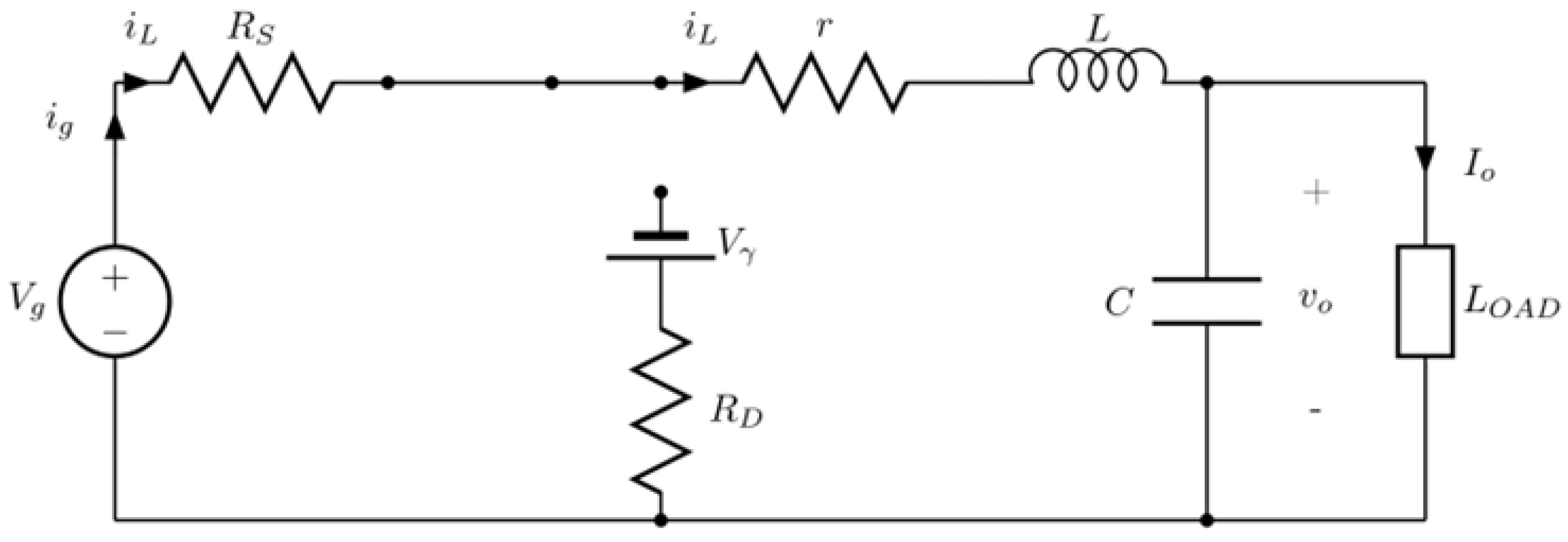
Figure 9.
Equivalent buck converter circuit for TON ≤ t ≤ TX.

Figure 10.
Buck-boost converter circuit with main non-idealities (losses).

Figure 11.
Equivalent buck-boost converter circuit for 0 ≤ t ≤ TON.

Figure 12.
Equivalent buck-boost converter circuit for TON ≤ t ≤ TX.
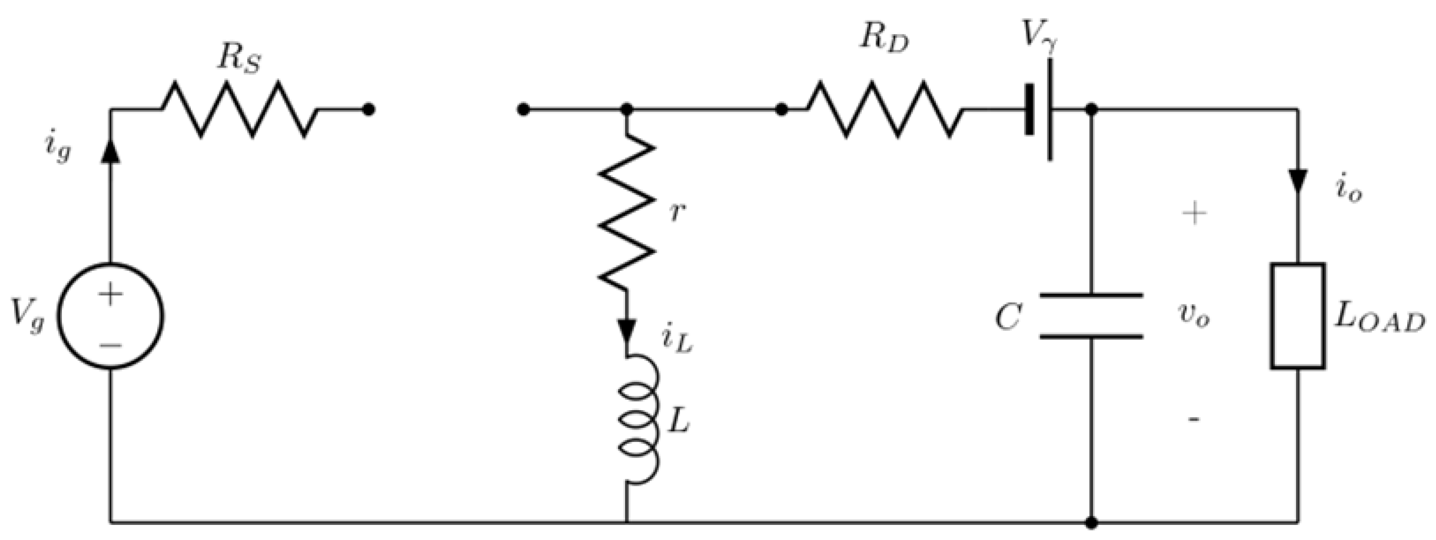
Figure 13.
PSpice simulation circuit for an actual boost converter.
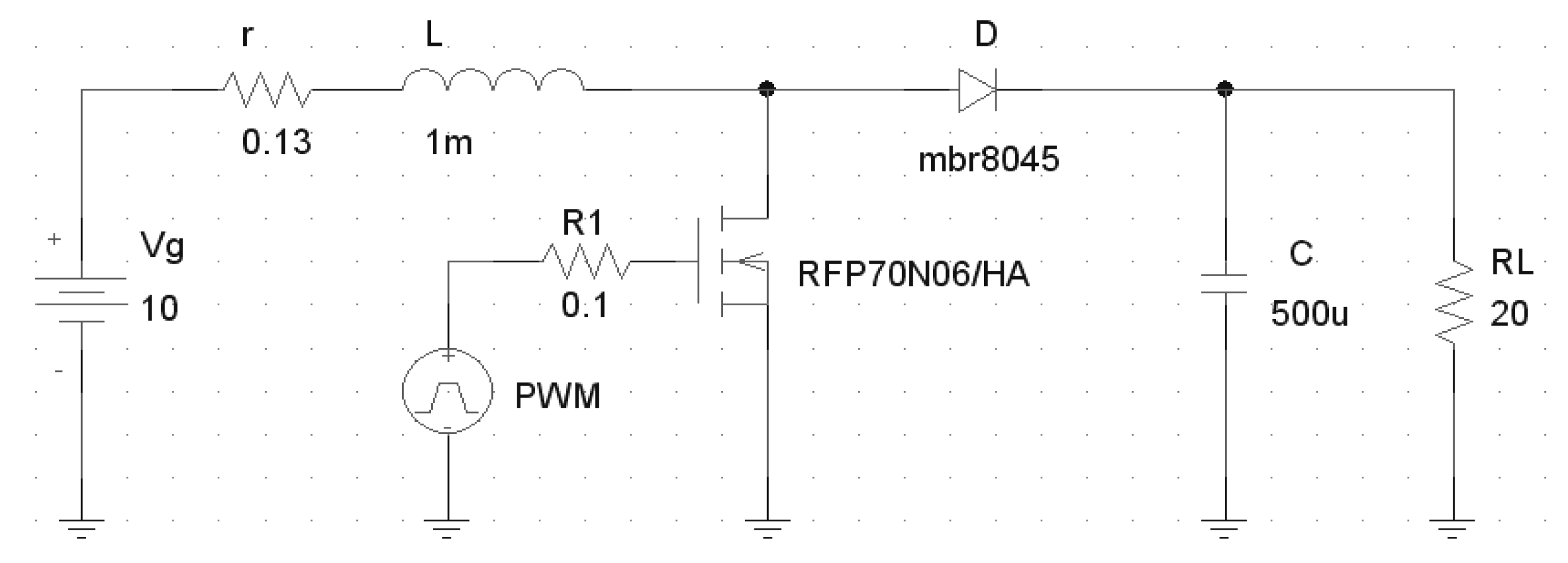
Figure 14.
PSpice simulation circuit for an actual buck converter.

Figure 15.
PSpice simulation circuit for an actual buck-boost converter.
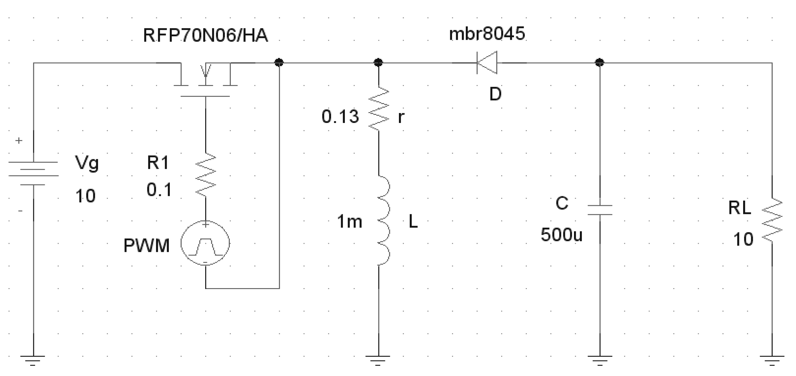
Figure 16.
Boost converter: voltage gain AVr.
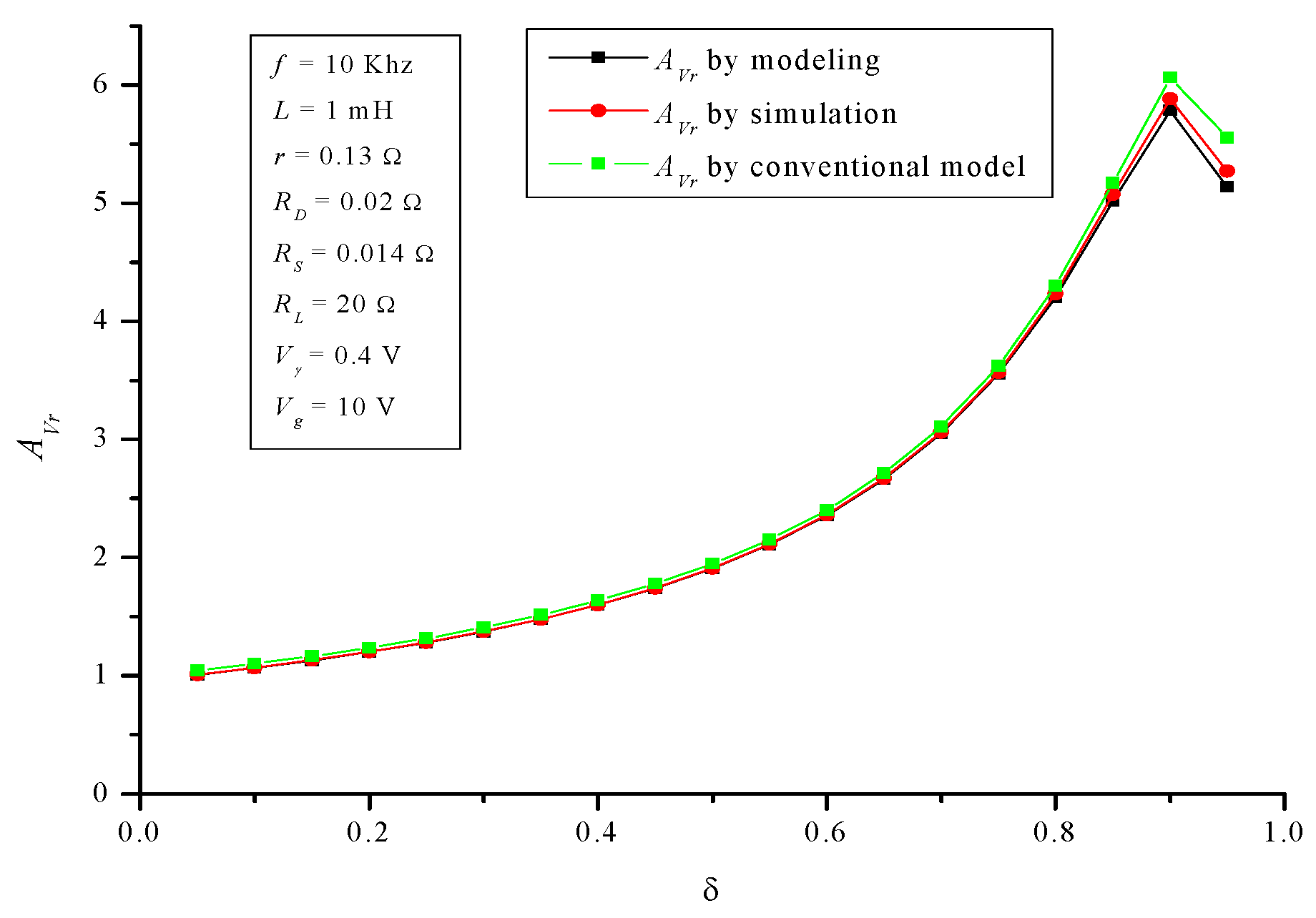
Figure 17.
Boost converter: input resistance Ri.

Figure 18.
Boost converter: efficiency η.
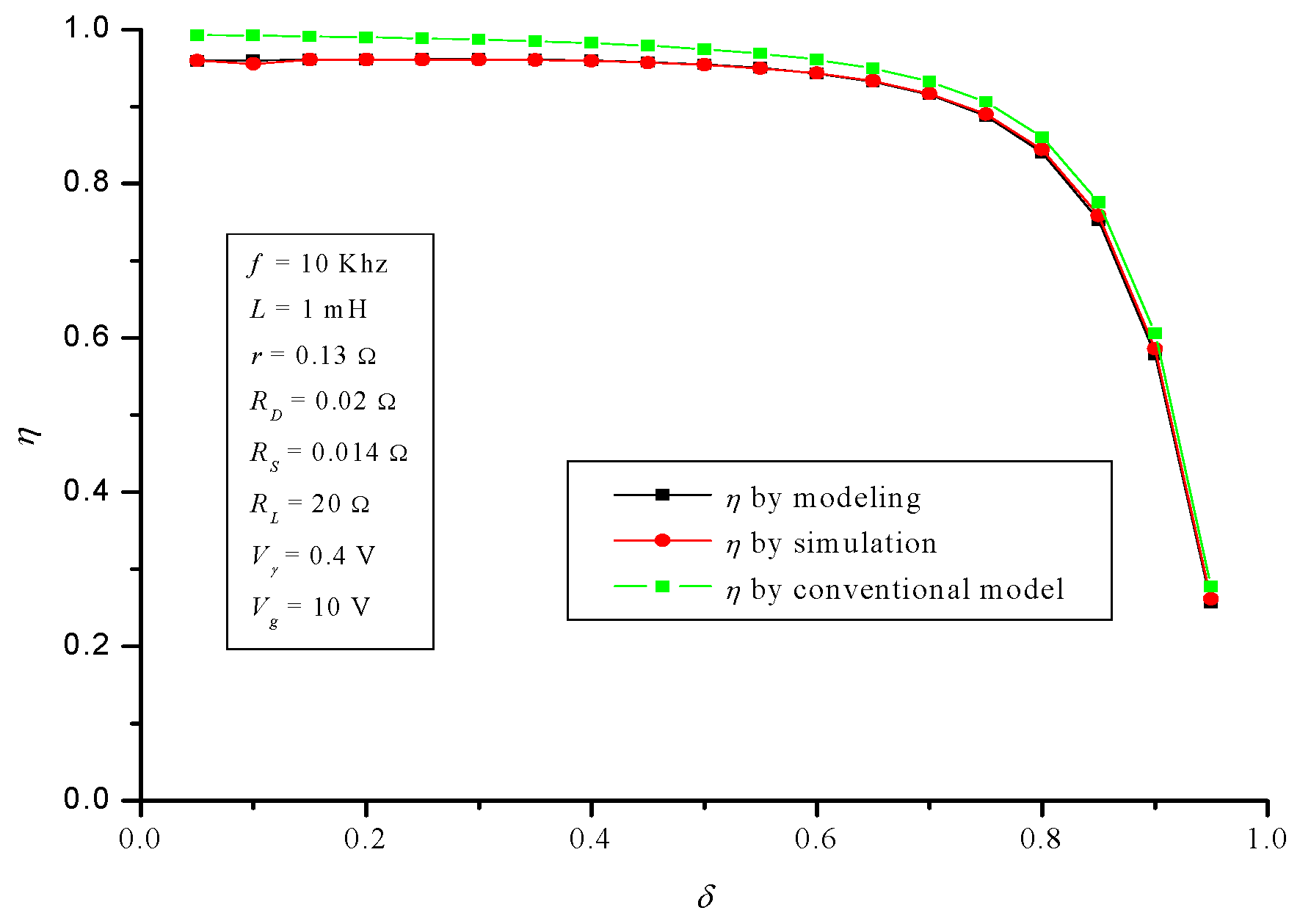
Figure 19.
Buck converter: voltage gain AVr.

Figure 20.
Buck converter: Input resistance Ri.
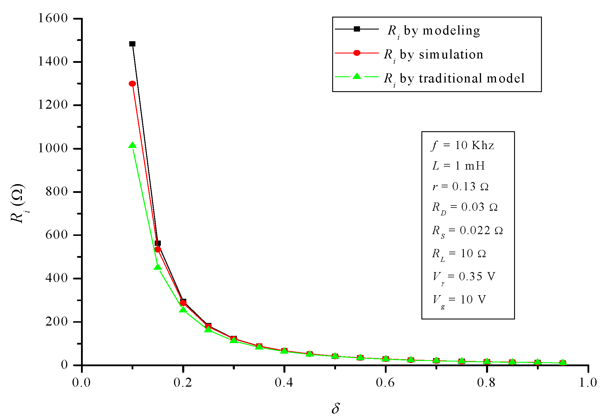
Figure 21.
Buck converter: efficiency η.
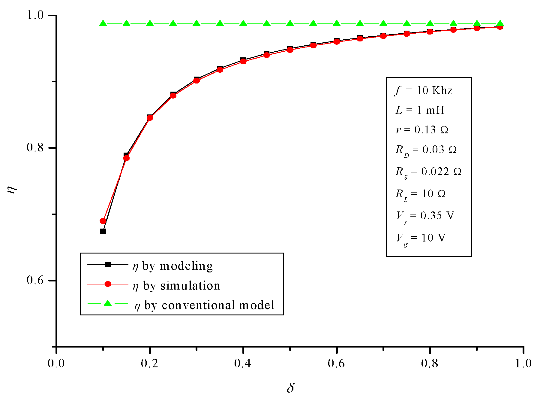
Figure 22.
Buck-boost converter: voltage gain AVr.

Figure 23.
Buck-boost converter: input resistance Ri.

Figure 24.
Buck-boost converter: efficiency η.

Table 1.
NMAE% for the developed and conventional models regarding the actual converters.
| Model | Converter | AVr | Ri | h |
|---|---|---|---|---|
| Developed | Boost | 0.45% | 0.66% | 0.30% |
| Buck | 0.73% | 1.61% | 0.31% | |
| Buck-boost | 1.4% | 1.98% | 0.84% | |
| Conventional | Boost | 2.93% | 2.19% | 2.69% |
| Buck | 7.10% | 5.39% | 8.09% | |
| Buck-boost | 7.57% | 5.87% | 8.65% |
Table 2.
Summary of the parameters for each DC/DC converter (see Figure 1).
Table 2.
Summary of the parameters for each DC/DC converter (see Figure 1).
| Parameter | Boost | Buck | Buck-boost |
|---|---|---|---|
| RX | |||
| VX | |||
| AVi | |||
| δf-crit | |||
| where: | |||
| For all converters: | |||
© 2017 by the authors. Licensee MDPI, Basel, Switzerland. This article is an open access article distributed under the terms and conditions of the Creative Commons Attribution (CC BY) license (http://creativecommons.org/licenses/by/4.0/).
Share and Cite
MDPI and ACS Style
Enrique, J.M.; Barragán, A.J.; Durán, E.; Andújar, J.M. Theoretical Assessment of DC/DC Power Converters’ Basic Topologies. A Common Static Model. Appl. Sci. 2018, 8, 19. https://doi.org/10.3390/app8010019
AMA Style
Enrique JM, Barragán AJ, Durán E, Andújar JM. Theoretical Assessment of DC/DC Power Converters’ Basic Topologies. A Common Static Model. Applied Sciences. 2018; 8(1):19. https://doi.org/10.3390/app8010019
Chicago/Turabian StyleEnrique, Juan Manuel, Antonio Javier Barragán, Eladio Durán, and José Manuel Andújar. 2018. "Theoretical Assessment of DC/DC Power Converters’ Basic Topologies. A Common Static Model" Applied Sciences 8, no. 1: 19. https://doi.org/10.3390/app8010019
Note that from the first issue of 2016, this journal uses article numbers instead of page numbers. See further details here.