Slot Waveguide Enhanced Bloch Surface Waves

Institute of Photonics, Department of Physics and Mathematics, University of Eastern Finland, P.O. BOX 111, 80101 Joensuu, Finland
Appl. Sci. 2018, 8(1), 39; https://doi.org/10.3390/app8010039
Submission received: 1 December 2017
/
Revised: 22 December 2017
/
Accepted: 26 December 2017
/
Published: 30 December 2017
(This article belongs to the Special Issue Surface Waves on Planar Photonic Crystals)
Abstract
:The paper presents a novel concept for the on-chip integration of a multilayer platform sustaining Bloch surface waves further enhanced by the so-called slot waveguide effect. Through simulations, we demonstrate that a carefully designed polymer waveguide arrangement coated with a subwavelength dielectric multilayer can be efficiently used to first excite a Bloch surface wave at the surface of the multilayer and second to enhance this wave and allow longer propagation of the surface mode by constructive superimposition of two evanescent tails inside a narrow gap.
1. Introduction
Bloch surface waves (BSWs) have already shown their potential as probes in sensing experiments [1,2,3]. The great advantages of such electromagnetic surface waves come from the all-dielectric platform on which they are generated [4] and from the long propagation length they offer compared to surface plasmon polaritons [5]. A BSW is created at the interface between a dielectric periodic medium and a homogeneous dielectric medium. A wave that is partially transmitted through a one-dimensional photonic crystal illuminated under an incidence angle greater than the critical angle is thus trapped between the two media and can only propagate along the surface.
Experimental and theoretical studies have been carried out these last few years on such waves. It has been demonstrated that exceptionally long propagation lengths can be achieved, that BSWs can be controlled using loading-strip on top of the platform, and that waveguides, ring resonators, photonic crystals, and gratings [6,7,8,9] can be used to control the direction and properties of these waves. The excitation of BSWs remains the principal issue in most of the current platforms. The most commonly employed technique is the Kretschmann configuration, which is the illumination through a prism, at an angle greater than the critical angle of the multilayer. Grating couplers have recently been successfully experimentally demonstrated [10]. However, no efficient on-chip solutions exist to excite a BSW so that the field is easily accessible for applications such as sensing.
In 2004, Almeida et al. demonstrated a novel concept of waveguide, i.e., the slot waveguide [11], enabling the propagation of light in a structure composed of two high refractive index rails separated by a thin air gap of a few tens of nanometers. This structure features a high confinement of the electric field in the air gap leading to a huge enhancement of the field in this region. One can consider, in a simplified scheme that this enhancement originates from the superimposition of the evanescent tails of the mode sustained by each rail.
The structure presented here combines these two concepts of Bloch surface waves and slot waveguides to create an on-chip platform allowing for excitation in a waveguide of the BSW, the enhancement of the surface wave, and a longer propagation thanks to its coupling to the slot mode. The concept is, in a sense, similar to the one proposed by R. Wang et al., who demonstrated the confinement of a BSW within a nanofiber, similar to a slab-slot waveguide [12]. Here, we propose an equivalent but in a vertical configuration and with air as material in the slot region. Moreover, the proposed geometry allows one to access the highly confined electromagnetic field for further sensing applications. The concept is demonstrated at λ = 488 nm, which is the excitation wavelength of a common fluorescent antibody (GFP, green fluorescent protein) used in the labeling of proteins for bio sensing.
2. Materials and Methods
Although this article is a theoretical study, it aims at demonstrating a concept, so simulations must be representative of a further fabrication. All dimensions, geometries, and materials are therefore realistic and can be fabricated and deposited.
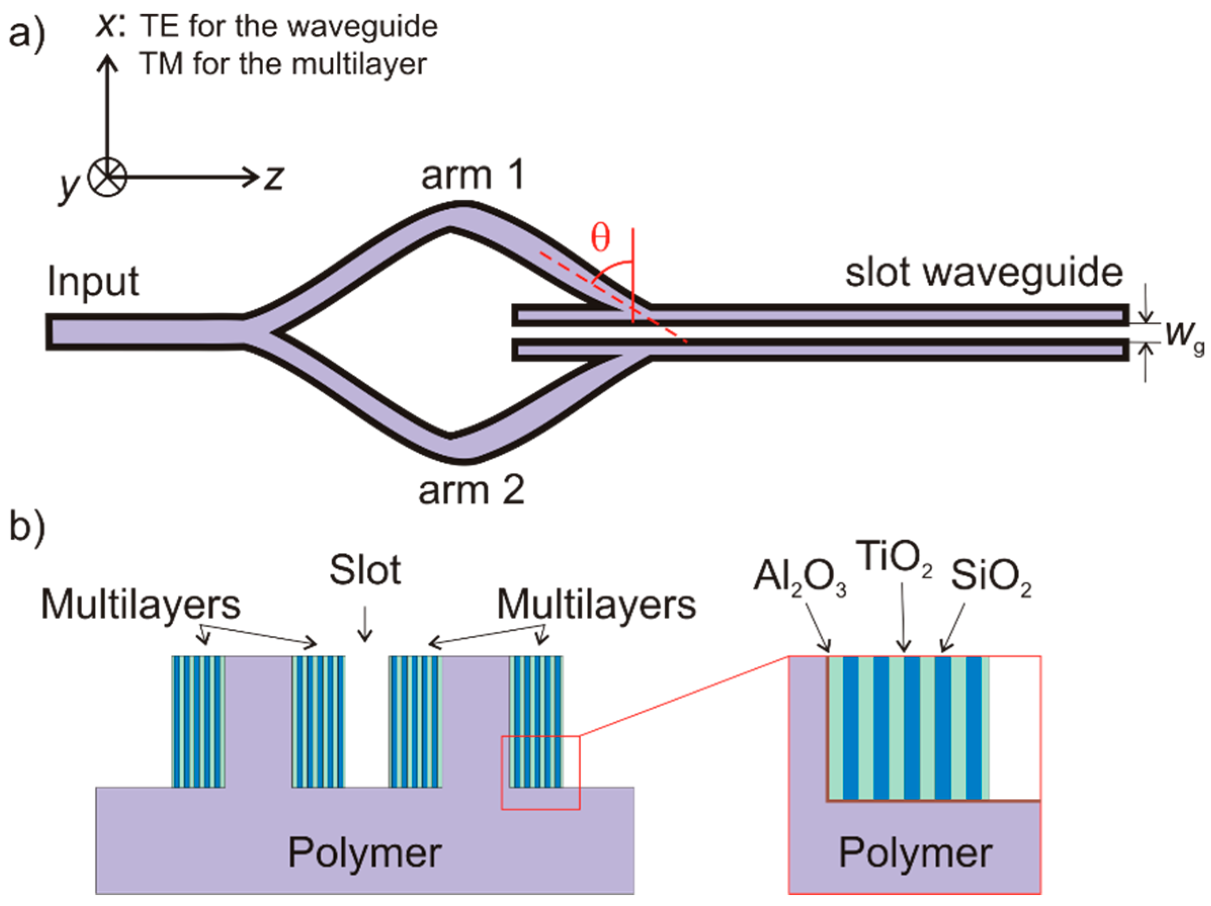
A sketch of the proposed structure is given in Figure 1. The structure is based on a polymer waveguide, e.g., the Ormocore® of refractive index np = 1.57 at λ = 488 nm. In a view to use a slot waveguide, the polarization is set to TE, i.e., the electric field is oriented parallel to the wafer plane in the x direction. It corresponds to the TM polarization when using the multilayer plane as a reference.
A large input waveguide of width win = 1 µm is separated into two thinner branches of width wb = 0.5 µm. These two branches enter the slot waveguide rail under an angle θ defined from the normal to the surface of the rails. The rail width is set to be wr = 0.5 µm and the slot width is wg = 70 nm. tL and tH are the respective thicknesses of the low and high refractive index layers.
2.1. Materials
Considering the existing fabrication processes, it is important to define the materials constituting the high and low refractive index layer. The low index material is intended to be silicon dioxide (SiO2, nL = 1.46 at λ = 488 nm) and the high refractive index is amorphous titanium dioxide (nH = 2.50 at λ = 488 nm). These two materials can be deposited conformally on the polymer basis using atomic layer deposition (ALD) [13,14]. The high refractive index contrast between the two materials allows for a smaller number of periods (N = 5, here), relaxing the fabrication but also reducing the total width of the waveguide.
The polymer, Ormocore® in this case, is chosen for its perfect compatibility with nano-imprinting techniques and its relatively high thermal stability (up to T = 270 °C). This second property is extremely important for the deposition of the ALD layers at a process temperature T = 120 °C [15].
2.2. Simulation Methods
The goal is to excite simultaneously two BSWs at the surface of the rails constituting the polymer slot waveguide. The input waveguide is split into two arms approaching the polymer rails under an angle θ. This angle must be greater than the critical angle in order to ensure both the propagation of light in the waveguide and the excitation of the BSW.
Preliminary simulations are performed using a transfer matrix method to estimate the reflection spectrum of the multilayer as a function of the incidence angle, the wavelength, the thicknesses of the layers, and the number of periods. As a starting point, we determine the critical angle which is for the proposed materials and considering TiO2 as the first deposited layer on the polymer around θc = 41°. Only the angles greater than θc are considered in the further calculations presented in the results section.
2.3. Towards Fabrication
Although experimental results are not presented in this article, it is important to consider the feasibility of the device and take into account the fabrication processes involved in the final realization of the structure. As already mentioned, the waveguide base is intended to be fabricated by means of the nano-imprinting of a silicon stamp, pattern by electron beam lithography, into an Ormocore® layer with a 500 nm thickness. The multilayer will be created using atomic layer deposition, which is a technique allowing a precise control of the layer thickness together with a highly conformal coating of the waveguides. The materials involved are TiO2 and SiO2, which can both be deposited by ALD using plasma-enhanced deposition. At this step, the multilayer is on the sides of the waveguide but also on top.
The multilayer has a higher average effective index than the waveguide, which yields a possibility for the hybrid BSW-slot waveguide mode to leak into this layer. To avoid this, a reactive ion etching of the top layers can be performed. The two materials constituting the multilayer can possibly be etched using the same gases, but at different rates. It leads a possibility to over etch the multilayer and damage the polymer waveguide. Ahmadi et al. have demonstrated recently that a thin layer (only few nanometers) of aluminum oxide can act as a perfect etch stop layer for this RIE processes, enabling the fabrication of coatings by ALD only on the vertical sides of waveguides [16,17]. With the refractive index of Al2O3 at this wavelength being nearly the same as that of the polymer, the response of the structure is not affected by this protective layer and allows for an etching of the top layers. As a result, only the sidewalls remains coated and the design structure can be fabricated.
It is important to remark that a layer nearly 1-µm-thick and composed of two materials has to be etched. Although it is feasible, it requires a careful adaptation of the processes in order to avoid rough surfaces and etching of the side layers.
3. Results
3.1. Multilayer
The optimization of the dielectric multilayer can be separated from the design of the slot waveguide although one will influence the other. The multilayer being the most sensitive, it is easier to adapt the slot waveguide than the BSW sustaining platform.
The multilayer is an alternating of titanium dioxide and silicon dioxide on a polymer substrate. The termination of the multilayer is of utmost importance to generate and tune the BSW. In the present case, a different thickness for the last TiO2 layer (thickness tlast) is considered. In addition to the different thicknesses involved in the structure, the angle of incidence has to be taken into account and is used to adjust the wavelength of the BSW mode at λ = 488 nm.
It is important to note at this early stage in the design that the different layers can be deposited by atomic layer deposition, which implies a control of the thickness at the nanometer scale. The two termination layers are used to precisely tune the resonance at the desired wavelength, and this can be done as a post-process step, as demonstrated by S. Paul et al. [18,19] recently.
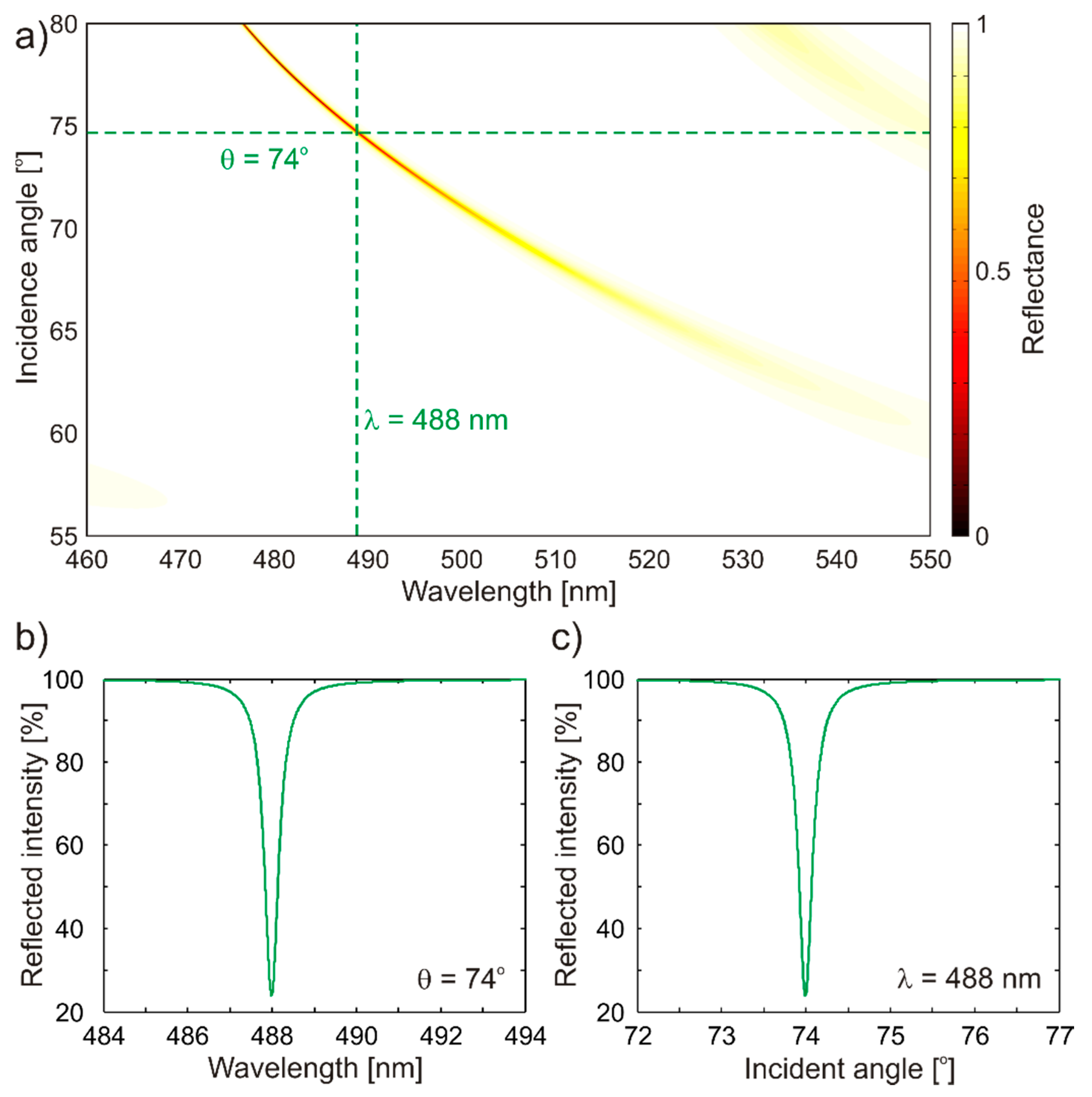
Figure 2 shows the simulation results obtained by the use of the transfer matrix method on the multilayer. The incident medium is the polymer—intended to be further fed by the waveguide mode—and the output medium is air, i.e., the slot region of the waveguide. The target is a BSW mode centered at λ = 488 nm. We consider a 5-period multilayer on top of which a last termination layer (high refractive index) is designed. The multilayer is illuminated under TM polarization, i.e., the electric field is in the plane of the wafer (see Figure 1). This polarization corresponds to the TE polarization for the slot waveguide. This is a crucial parameter since slot waveguides confine the electric component of a quasi-TE polarized mode in the low index region gap (here, air). However, one can also excite a TE BSW, leading to only a weak confinement of the field inside the slot waveguide.
The reflectance spectrum and its dependence with the angle of incidence is presented in Figure 2a. A zoom-in on the BSW mode is shown in Figure 2b as a function of the wavelength and in Figure 2c as a function of the incidence angle. For λ = 488 nm, the incidence angle is θ = 74°. The layer thicknesses are tH = 90 nm and tL = 120 nm. The multilayer is terminated by a last high refractive index layer of thickness tlast = 80 nm. The extinction ratio is about 75%.
3.2. Waveguide Integration
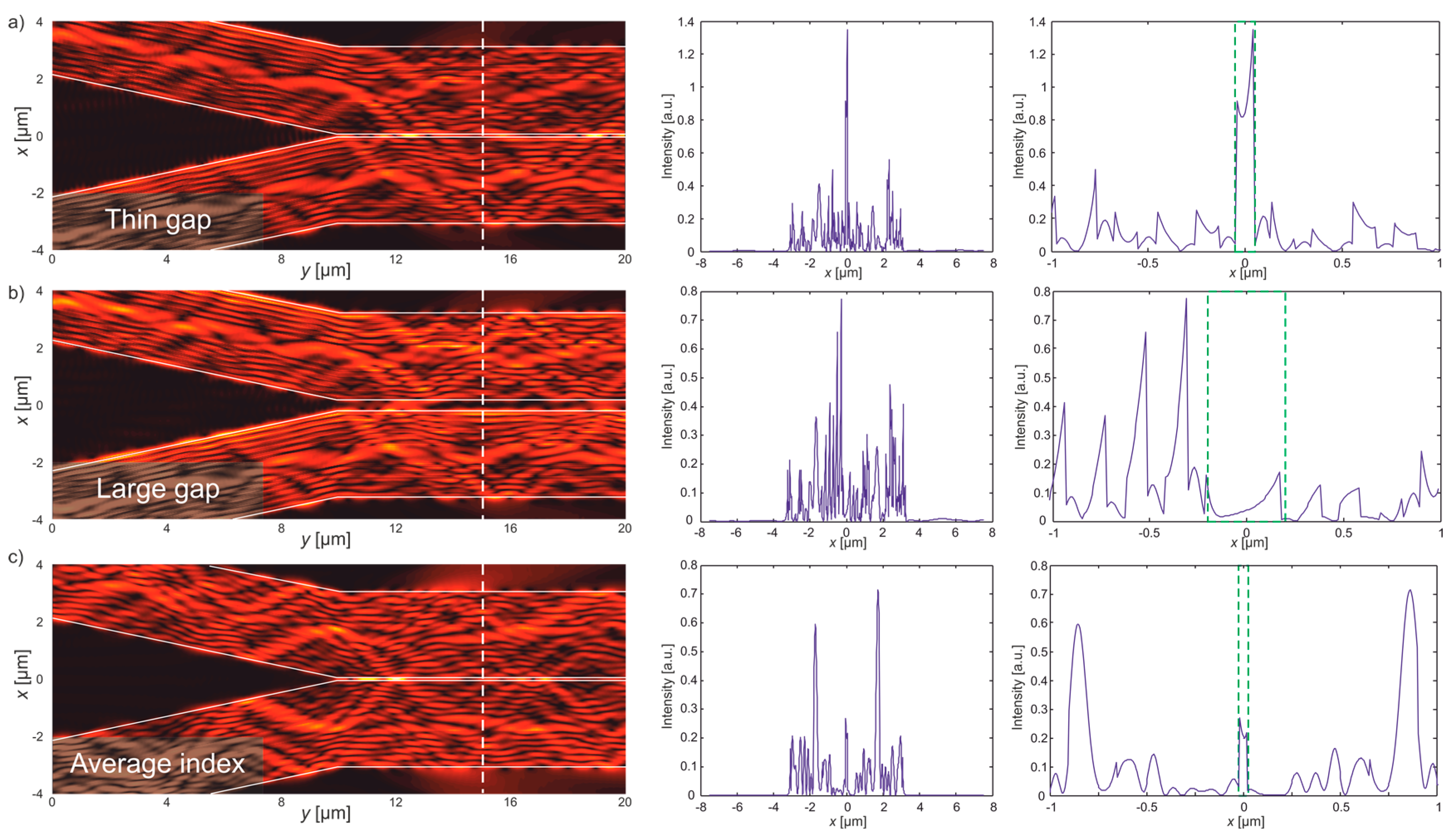
Simulations of the waveguide including the multilayer are performed using a commercial software based on the finite difference time domain method (OptiFDTD by OptiWave). The intensity distribution of the major field component () is shown in Figure 3 together with the field profile along x for three cases. Figure 3a corresponds to a slot waveguide gap of wg = 70 nm, which is the ideal case. Figure 3b is the distribution for wg = 400 nm, i.e., a far too large gap to enable the slot enhancement coming from the superimposition of the two BSW evanescent tails. Figure 3c is used as a comparison structure. It is identical in terms of geometry to the structure presented in Figure 3a, but the multilayer is replaced by a material of refractive index n = 1.91, equivalent to the average refractive index of the multilayer ().
One can see, in the case where wg = 70 nm, that the electric field is confined in the slot region as expected, which is not the case when wg = 400 nm. The field intensity distributions show the coupling zone between the feeding waveguides and the slot waveguide. It is clear that the evanescent tail of the BSW modes are not overlapping for large gaps, while a field confinement in the air slot is observed for thinner gaps smaller than the characteristic length Lc = 155 nm, calculated considering the propagation constant of the BSW and the refractive index of the output medium (air) [20]. The field remains mainly inside the multilayer as shown in Figure 3b.
The modal field profile shown in Figure 3a (wg = 70 nm) shows the classical cosh shape of the mode characteristic of a slot waveguide and coming from the sum of two evanescent waves with opposite signs. In Figure 3a, it is evident that the useful part of the field is inside the air region of the slot waveguide, while only the evanescent part of the field is accessible in case of a large gap. This second configuration is actually similar to the classical BSW platform illuminated using the Kretschmann configuration.
The extinction ratio of 75% of the BSW yields to a back-reflection by the multilayer in the waveguide and therefore leakage inside the polymer device. However, since the whole structure is covered by the multilayer, one can see consecutive reflections inside the waveguide, always at the excitation angle of the BSW. The mechanism is similar to that observed in the case of an ARROW device (anti-reflective resonant waveguide). It follows that at each reflection the BSW is re-excited all along the slot waveguide. Such a mechanism leads to a dashed propagation inside the slot region. A trade-off must be found between a too high reflectivity allowing for a thin BSW, and a too low reflectivity leading to high losses. Finally, the output shape of the feeding waveguides, i.e., the two arms of the split input waveguide, has to be carefully designed in order to avoid injection of light inside the multilayer itself.
For comparison, a third simulation has been performed on a polymer slot waveguide structure (wg = 70 nm) covered by a homogeneous material of refractive index n = 1.91. Results are presented in Figure 3c. One can clearly see the characteristic intensity distribution corresponding to a slot waveguide (right graph) but at a lower intensity than in Figure 3a. Note that in a classical slot waveguide scheme (only one material constituting the rails), the enhancement, coming from the field discontinuity at the interface, is proportional to , where n is the refractive index of the rail medium. Increasing the refractive index of the rails leads to an increase of the slot effect. Between the cases presented in Figure 3a,c, the multilayer is replaced by a lower refractive index than TiO2. Considering here, that the observed decreased intensity in the gap is only due to the change of material, a ratio of about 1.7 should be measured. However, the maximum intensity reaches a level much lower than in the case of the multilayer. It proves an enhancement of about 5 of the slot effect, which is due to the superimposition of the BSWs.
4. Conclusions
The goal of this study is to demonstrate the potential integration of BSW platforms in on-chip devices. Utilizing the concept of slot waveguide fed with tilted waveguides opens the premise of novel devices and even higher enhancement easily accessible because of the field confinement in the air region of the slot waveguide. One can therefore admit that an analyte, supposed to be in this particular case a fluorescent biomarker absorbing at λ = 488 nm, placed in the slot waveguide will overlap more with the guided mode. Sensor based on this concept are intended to exhibit a higher sensitivity than classical slot waveguide or classical BSW-based sensors.
Acknowledgments
This work was funded by the Finnish Funding Agency for Technology and Innovation (Tekes) under the FiDi Pro Project NP Nano (grant 40315/13). The authors wish to thank Seppo Honkanen and Pertti Pääkkönen for their useful comments and discussions.
Conflicts of Interest
The author declare no conflict of interest. The founding sponsors had no role in the design of the study; in the collection, analyses, or interpretation of data; in the writing of the manuscript; or in the decision to publish the results.
References
- Shinn, M.; Robertson, W.M. Surface plasmon-like sensor based on surface electromagnetic waves in a photonic band-gap material. Sens. Actuators B Chem. 2005, 105, 360–364. [Google Scholar] [CrossRef]
- Paeder, V.; Musi, V.; Hvozdara, L.; Herminjard, S.; Herzig, H.P. Detection of protein aggregation with a Bloch surface wave based sensor. Sens. Actuators B Chem. 2011, 157, 260–264. [Google Scholar] [CrossRef]
- Sinibaldi, A.; Danz, N.; Descrovi, E.; Munzert, P.; Schulz, U.; Sonntag, F.; Dominici, L.; Michelotti, F. Direct comparison of the performance of Bloch surface wave and surface plasmon polariton sensors. Sens. Actuators B Chem. 2012, 174, 292–298. [Google Scholar] [CrossRef]
- Yeh, P.; Yariv, A.; Cho, A.Y. Optical surface waves in periodic layered media. Appl. Phys. Lett. 1978, 32, 104–105. [Google Scholar] [CrossRef]
- Dubey, R.; Barakat, E.; Häyrinen, M.; Roussey, M.; Honkanen, S.K.; Kuittinen, M.; Herzig, H.P. Experimental investigation of the propagation properties of Bloch surface waves on dielectric platform. J. Eur. Opt. Soc. Rapid Publ. 2017, 13, 5. [Google Scholar] [CrossRef]
- Descrovi, E.; Sfez, T.; Quaglio, M.; Brunazzo, D.; Dominici, L.; Michelotti, F.; Herzig, H.P.; Martin, O.J.F.; Giorgis, F. Guided bloch surface waves on ultrathin polymeric ridges. Nano Lett. 2010, 10, 2087–2091. [Google Scholar] [CrossRef] [PubMed]
- Yu, L.; Barakat, E.; Sfez, T.; Hvozdara, L.; Di Francesco, J.; Peter Herzig, H. Manipulating Bloch surface waves in 2D: A platform concept-based flat lens. Light Sci. Appl. 2014, 3, e124. [Google Scholar] [CrossRef]
- Dubey, R.; Vosoughi Lahijani, B.; Häyrinen, M.; Roussey, M.; Kuittinen, M.; Herzig, H.P. Ultra-thin Bloch-surface-wave-based reflector at telecommunication wavelength. Photonics Res. 2017, 5, 494–499. [Google Scholar] [CrossRef]
- Kim, M.-S.; Vosoughi Lahijani, B.; Descharmes, N.; Straubel, J.; Negredo, F.; Rockstuhl, C.; Häyrinen, M.; Kuittinen, M.; Roussey, M.; Herzig, H.P. Subwavelength focusing of Bloch surface waves. ACS Photonics 2017, 4, 1477–1483. [Google Scholar] [CrossRef]
- Kovalevitch, T.; Boyer, P.; Suarez, M.; Kim, M.-S.; Herzig, H.P.; Bernal, M.-P.; Grosjean, T. Polarization controlled directional propagation of Bloch surface wave. Opt. Express 2017, 25, 5710–5715. [Google Scholar] [CrossRef] [PubMed]
- Almeida, V.R.; Xu, Q.; Barrios, C.A.; Lipson, M. Guiding and confining light in void nanostructure. Opt. Lett. 2004, 29, 1209–1211. [Google Scholar] [CrossRef] [PubMed]
- Wang, R.; Xia, H.; Zhang, D.; Chen, J.; Zhu, L.; Wang, Y.; Yang, E.; Zang, T.; Wen, X.; Zou, G.; et al. Bloch surface waves confined in one dimension with a single polymeric nanofibre. Nat. Commun. 2017, 8, 14330. [Google Scholar] [CrossRef] [PubMed]
- Puurunen, R.L. A short history of atomic layer deposition: Tuomo Suntola’s atomic layer epitaxy. Chem. Vap. Depos. 2014, 20, 332–344. [Google Scholar] [CrossRef]
- Autere, A.; Karvonen, L.; Säynätjoki, A.; Roussey, M.; Färm, E.; Kemell, M.; Tu, X.; Liow, T.Y.; Lo, G.Q.; Ritala, M.; et al. Slot waveguide ring resonators coated by atomic layer deposited organic/inorganic nanolaminate. Opt. Express 2015, 23, 26940–26951. [Google Scholar] [CrossRef] [PubMed]
- Hiltunen, M.; Hiltunen, J.; Stenberg, P.; Aikio, S.; Kurki, L.; Vahimaa, P.; Karioja, P. Polymeric slot waveguide interferometer for sensor applications. Opt. Express 2014, 22, 7229–7237. [Google Scholar] [CrossRef] [PubMed]
- Ahmadi, L.; Tervo, J.; Saarinen, J.; Honkanen, S. Enhanced sensitivity in polymer slot waveguides by atomic layer deposited bylayer coatings. Appl. Opt. 2013, 52, 8089–8094. [Google Scholar] [CrossRef] [PubMed]
- Ahmadi, L.; Hiltunen, M.; Stenberg, P.; Roussey, M.; Saarinen, J.; Honkanen, S. ALD-coated polymer slot waveguide young interferometer. Opt. Express 2016, 24, 10275–10285. [Google Scholar] [CrossRef] [PubMed]
- Paul, S.; Vartiainen, I.; Roussey, M.; Saastamoinen, T.; Tervo, J.; Honkanen, S.; Kuittinen, M. Add-drop filter based on TiO2 coated shifted Bragg grating. Opt. Express 2016, 24, 26901–26910. [Google Scholar] [CrossRef] [PubMed]
- Paul, S.; Saastamoinen, T.; Honkanen, S.; Roussey, M.; Kuittinen, M. Multi-wavelength filtering with waveguide integrated quasi-random Bragg grating. Opt. Lett. 2017, 42, 4635–4638. [Google Scholar] [CrossRef] [PubMed]
- Pélisset, S.; Laukkanen, J.; Kuittinen, M.; Honkanen, S.; Roussey, M. Modal properties of a strip-loaded horizontal slot waveguide. J. Eur. Opt. Soc. Rapid Publ. 2017, 13, 37. [Google Scholar] [CrossRef]
Figure 1.
Schematic representation of the proposed waveguide structure for BSW excitation and confinement. (a) Top view of the entire device including the input waveguide, the Y-junction splitter, and the slot waveguide. The solid thick black curve represents the multilayer; (b) Cross section of the polymer slot waveguide coated with a multilayer. The inset is a close up of the multilayer, which is a periodic arrangement of a low and high refractive index material terminated by a finely tuned layer (high refractive index).

Figure 2.
(a) Spectral and angular reflection spectrum of the multilayer calculated by transfer matrix method. The green dashed lines represent the target wavelength (λ = 488 nm) and the corresponding angle of incidence (θ = 74°); (b) Wavelength dependence of the reflectivity on the multilayer; (c) Angle dependence of the reflectivity. All calculations are performed under TM illumination (TE in the waveguide referential) according to notations Figure 1.

Figure 3.
Intensity distribution (left) and intensity mode profile (corresponding to the white dashed lines) of the major field component Ex (right) for (a) a thin gap wg = 70 nm for the slot waveguide, (b) for a larger gap wg = 400 nm, and (c) for a 70 nm gap structure where the multilayer is replaced by a homogeneous material of average refractive index n = 1.91. The far-right column displays zoom-in on the slot regions, which are delimited by green dashed rectangles.
© 2017 by the author. Licensee MDPI, Basel, Switzerland. This article is an open access article distributed under the terms and conditions of the Creative Commons Attribution (CC BY) license (http://creativecommons.org/licenses/by/4.0/).
Share and Cite
MDPI and ACS Style
Roussey, M. Slot Waveguide Enhanced Bloch Surface Waves. Appl. Sci. 2018, 8, 39. https://doi.org/10.3390/app8010039
AMA Style
Roussey M. Slot Waveguide Enhanced Bloch Surface Waves. Applied Sciences. 2018; 8(1):39. https://doi.org/10.3390/app8010039
Chicago/Turabian StyleRoussey, Matthieu. 2018. "Slot Waveguide Enhanced Bloch Surface Waves" Applied Sciences 8, no. 1: 39. https://doi.org/10.3390/app8010039
Note that from the first issue of 2016, this journal uses article numbers instead of page numbers. See further details here.