Broadband Electromagnetic Dipole Resonance by the Coupling Effect of Multiple Dielectric Nanocylinders

1
College of Metrology & Measurement Engineering, China Jiliang University, Hangzhou 310018, China
2
Institute of Optoelectronic Technology, China Jiliang University, Hangzhou 310018, China
*
Author to whom correspondence should be addressed.
Appl. Sci. 2018, 8(1), 60; https://doi.org/10.3390/app8010060
Submission received: 30 November 2017
/
Revised: 26 December 2017
/
Accepted: 27 December 2017
/
Published: 3 January 2018
(This article belongs to the Special Issue Sub-wavelength Optics)
Abstract
:Broadband resonant scattering in a visible region that can be obtained by coupled multiple silicon nanocylinders. For a single high refractive index silicon nanocylinder, the electric dipole and magnetic dipole resonances can be observed. By constructing a silicon nanocylinder dimer, the interaction between the particles plays an important role in broadband scattering. Interestingly, due to magnetic-magnetic dipole interaction, a splitting phenomenon of magnetic resonance mode is revealed. A new magnetic resonant mode emerges at a longer wavelength in dimer and trimer by changing the diameter of one nanocylinder in dimer or trimer, and the gap size between nanocylinders. The scattering bandwidth can further increase with the effect of substrate, which is attributed to the extension of resonant mode into substrate. The broadband optical response can be revealed by the calculated scattering resonant spectra and the spatial electromagnetic field distributions. Furthermore, the transmission of periodic nanocylinder structure, including single nanocylinder and dimer, is demonstrated. By decreasing the gap between nanocylinders in dimer for periodic array structure, a new electric resonant mode occurs. These results can provide a guideline to realize broadband resonant optical elements.
1. Introduction
With the rapid development of information technology, the requirement of components tends to be miniaturized and integrated. But, due to the limitation of the diffraction limit, the traditional optoelectronic components in nano-size can not get effective photoelectric information dissemination and utilization. Then, the nanophotonics become a hot research field. For example, the resonant nanostructures [1] have a large scattering cross-section [2], and they can concentrate, redirect, and manipulate light [3,4] at the surface of many optical devices [5], such as solar cells [6,7], sensors, etc. They can also optimize the coupling and capture of light. In recent decades, some considerable researches have focused on the design, construction, and synthesis of different plasma nanostructures [8,9], such as nanorods, nanoshells, nanocyclic rings, nanoscale [10], nanowires, and nano crescents. As a kind of nano-scale optical control method, plasma resonance [11] of metal nanostructures has attracted much attention in optical, biomedical, and nonlinear materials.
However, the metal nanostructure has a small dielectric constant and a large non-radiation loss (such as ohmic loss) [12,13,14]. So, its related application performance is limited to further develop, especially in visible region. In general, the intrinsic dielectric constant of the dielectric material is large, and the non-radiation loss is very low. So, dielectric material with a high refractive index can effectively suppress the radiation loss and non-radiation loss to construct the nanostructure with low absorption loss [15]. Dielectric nanostructured materials with a high refractive index have recently risen to prominence for the control of light [16]. They give a novel way to directly engineer electromagnetic field response at optical frequencies. Specially, these high refractive index nanoparticles can be designed to a new building block for scalable, tunable, and low-loss metamaterials [17]. A single dielectric spherical nanoparticle exhibited both magnetic dipole and magnetic dipole resonances. Unlike plasmonic nanoparticles, the magnetic resonance, demonstrated in silicon [18] and gallium arsenide nanoparticles [19], results from circular displacement currents that are driven by an incident electric field. However, most researches have concentrated upon single nanoparticle or periodic structure [3,8,9,13]. Recently, nanodimer nanoparticles can offer further tunability and engineering capabilities for electric dipole or magnetic dipole resonances [20,21]. Also, it can reveal the physics of hotspots and near-field distributions, which is important for nanoparticles with Fano-type resonances and strong interparticle interactions [17,20,21]. Dimer nanoparticles with high refractive index materials have recently been studied in numerical calculations [22,23] and in experiments at microwave frequencies [24,25]. Dielectric nanoparticles can reduce quenching and provide higher quantum efficiency of localized emitters, which is important for engineering emission at the subwavelength scale [22]. Thus, dielectric nanoparticles can be frequently applied in efficient magnetic scatterers [26], with possible application in metamaterials [27], metasurfaces [28], nanoantennas [29], and optical on-chip integration devices exhibiting unusual scattering properties [30].
In this paper, we systematically studied the resonant scattering and coupling properties of multiple dielectric nanocylinders in visible spectrum. The resonant performances of nanostructures composed of one, two, or three silicon nanocylinders are demonstrated numerically by finite difference time domain method [31]. We also studied the transmission characteristics and resonance of the periodic arrays of the nanocylinder structure. By adjusting the geometric parameters of silicon nanocylinder arrays, the electric dipole and magnetic dipole resonances can be selectively enhanced or suppressed for different applications.
2. Theoretical Modal of Coupled Nanoparticles
When the feature size of the high refractive index dielectric nanoparticles is significantly smaller than the incident wavelength, the resulting optical resonance can be described by the effective electric dipole and magnetic dipole as [32]:
where and denote the induced electric and magnetic dipoles, respectively, and and are the electric and magnetic polarizabilities, respectively, and and are the incident fields.
When considering the interaction between multiple nanoparticles, the electric and magnetic fields at the ith particle, as caused by the jth particle, can be represented by [32]
where denote the direction vector from the jth particle to ith particle. The coefficients aij, bij and dij are expressed as:
where rij denotes the distance between ith and jth particles and k = 2π/λ. Thus, the total induced electric and magnetic dipoles can be derived as [32]:
where represents the speed of light in vacuum. When , and → 0 with → ∞, the electric and magnetic dipoles can be regarded as equivalent to that of a single nanoparticle. When → 0, the scattering characteristics changes dramatically. According to Equation (4), the electric-to-electric interaction, the electric-to-magnetic interaction, and the magnetic-to-magnetic interaction can be found. The coupled nanoparticles can achieve versatile functions by these induced interactions.
3. Resonant Scattering of Nanocylinders
3.1. Scattering Characteristics of Single Nanocylinder
The schematic of nanocylinder is shown in Figure 1. The light source is incident from the top of the nanocylinder particle. The displacement current can be formed in nanocylinder by the electric field of the incident light, resulting in the formation of the in-plane magnetic dipole [18,19,20]. Silicon material for nanocylinder is used because it is a high refractive index material with a relatively low absorption loss in the visible spectrum range, and it is compatible to nanophotonic devices and semiconductor components. In our simulation, the total field scattering field (TFSF) light source of finite-difference time-domain method (FDTD) was applied as the excitation source. The scattering cross-section and the electromagnetic field distribution of the nanocylinder or nanocylinder array were accurately calculated by FDTD method.
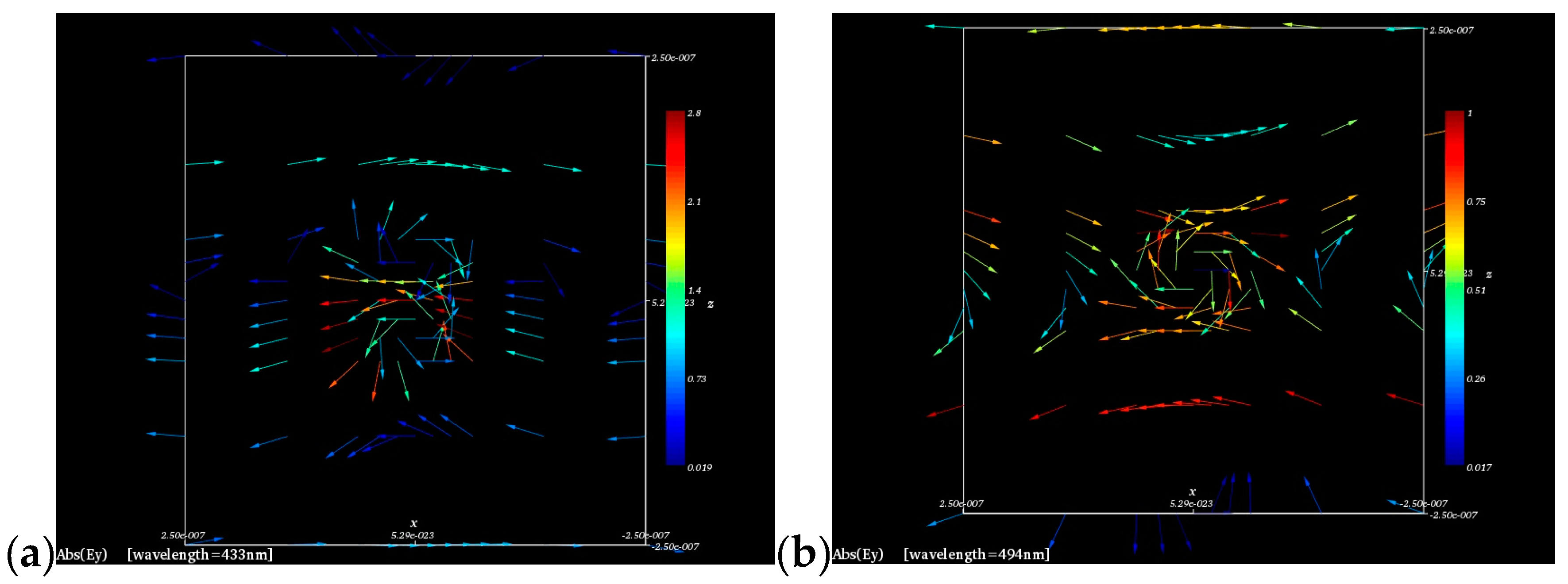
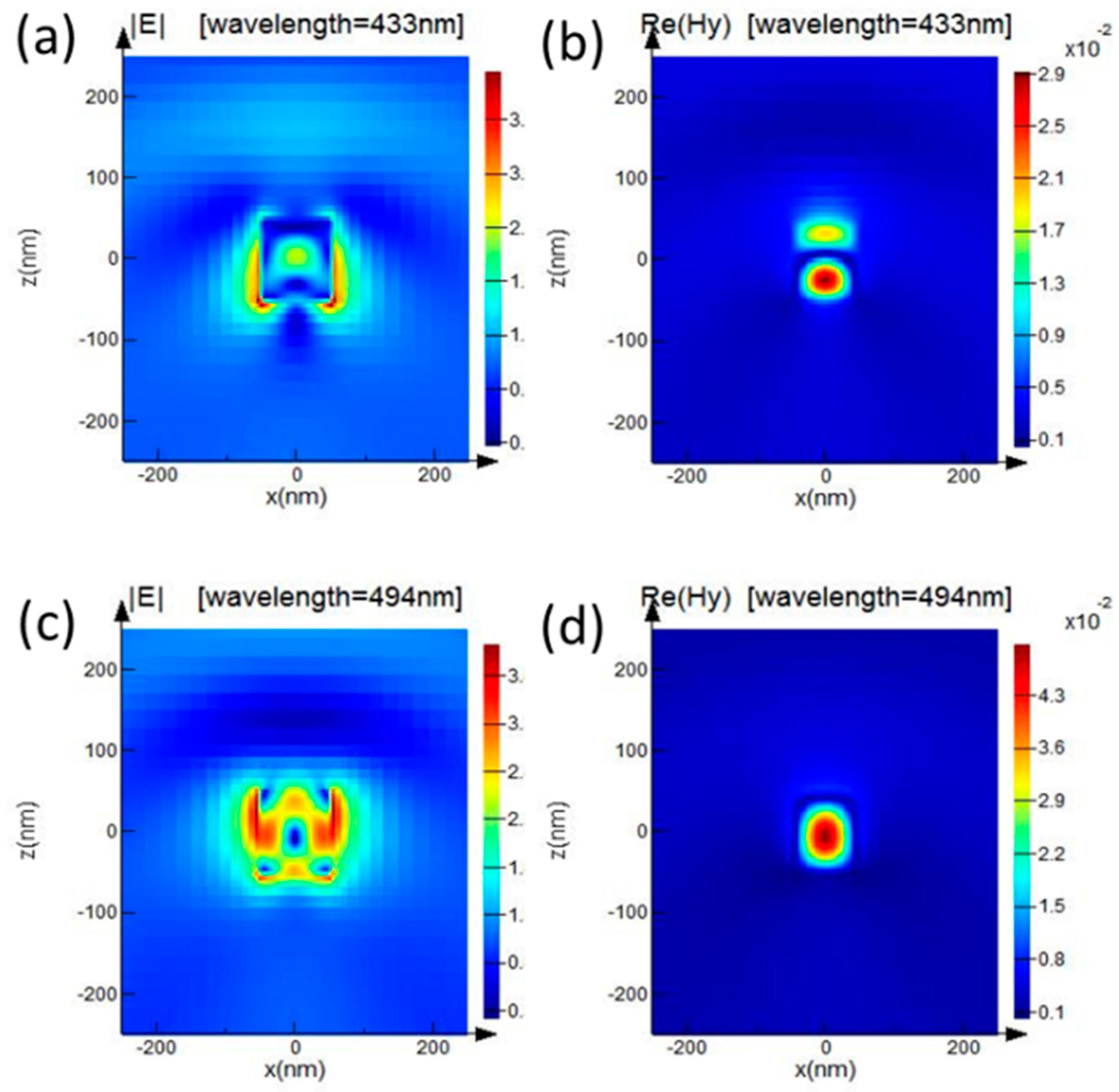
Firstly, we study the scattering properties of single nanocylinder, as in Figure 2. is defined as the scattering cross-section of a single silicon nanocylinder in air. The scattering cross section for a silicon nanocylinder with height and diameter of 100 nm is demonstrated. It can be seen that the scattering peaks are at 433 nm and 494 nm, respectively. We can use the field profiles inside the nanocylinder to identify the electromagnetic resonant modes and the corresponding current loops in Figure 3. Figure 3 shows the electric field vector distribution at the center of nancylinder. It can be revealed that the resonant mode at corresponds to the electric dipole (ED) mode, and the resonant mode at corresponds to the magnetic dipole (MD) mode based on the field lines loop induced by the driving field. In order to further reveal electromagnetic field characteristics of nanocylinder, the electromagnetic field distribution in Figure 4 is plotted at and , respectively. From the electric field distribution in Figure 4a, a linear electric field distribution in the center of nanocylinder at is shown, and there is a displacement current loop with the circulating electric field at in Figure 4c. From the magnetic field distribution, there is a node at the center at in Figure 4b, which indicates the presence of electric dipole. There is an antinode at the center at in Figure 4d, which is consistent with a magnetic dipole. By the vector field lines and the electromagnetic field distributions, it can be revealed that the scattering resonant mode at can be attributed to the electric resonance, and the scattering resonant mode at originates from magnetic resonance.
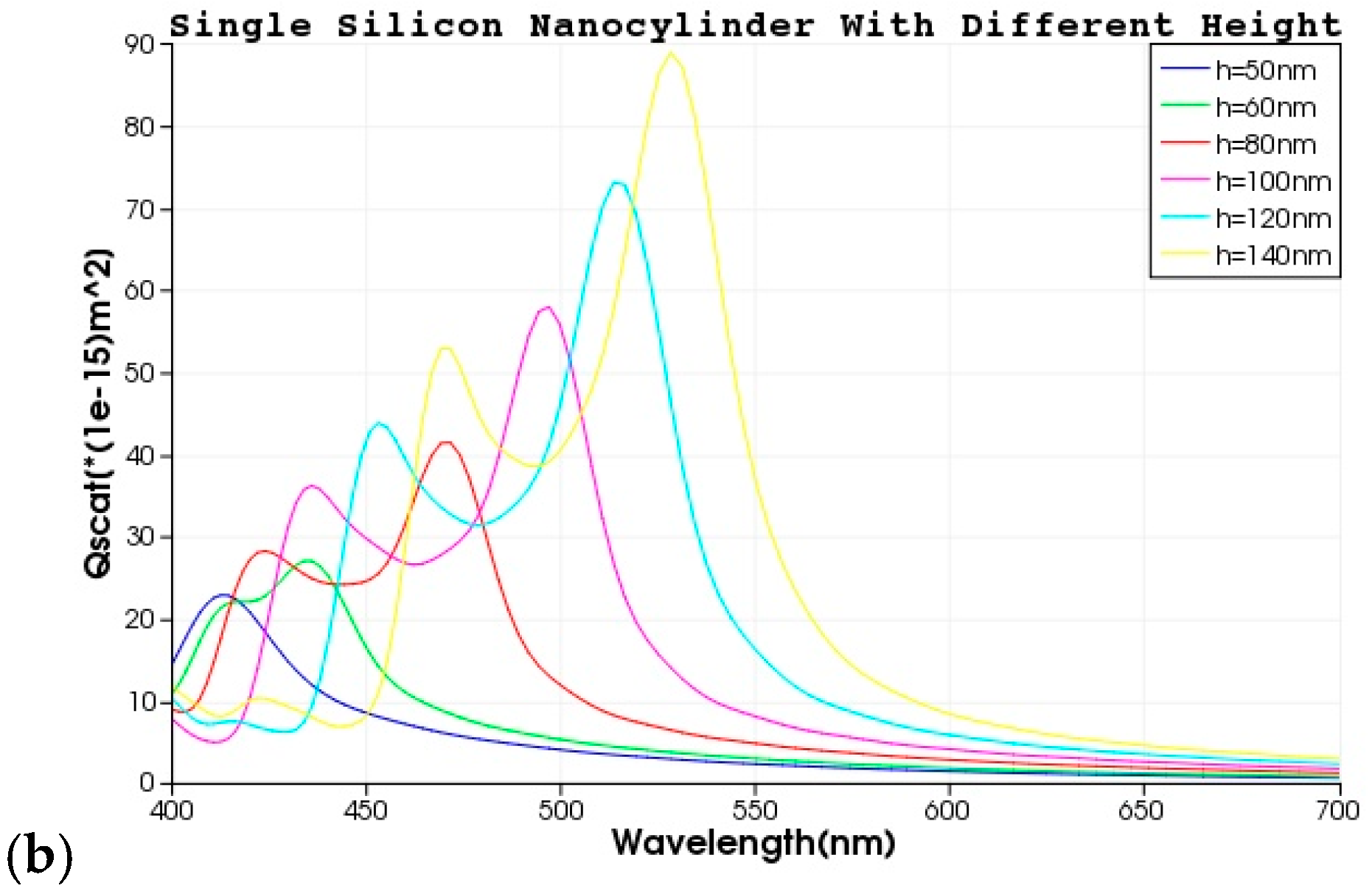
Figure 5a shows the scattering spectra for particle radius from 50 nm to 70 nm, with the height of 100 nm. It can be seen that the scattering resonant modes, ED and MD, show a clear red-shift and an increase in for increasing nanocylinder diameter. For the diameter of 140 nm, the higher order mode of electric duadrupole occurs at visible spectrum. In Figure 5b, the influence of particle height with diameter of 100 nm to scattering resonance is shown. With the increase of height, the two maxima of the scattering cross-section show a clear redshift, and the amplitude increases. For the nanocylinder with a height of 50 nm, it is not sufficient to support the MD mode, so the amplitude of MD resonance is smaller. It is expected that MD resonance can not be supported if the height of particle is too shallow to drive the displacement current loop. Also, since inside and outside the particle, the magnetic current loop that is caused by the dipole moment can extend to the outside of the particle.
3.2. Scattering Characteristics of Double-Nanocylinders-Combination
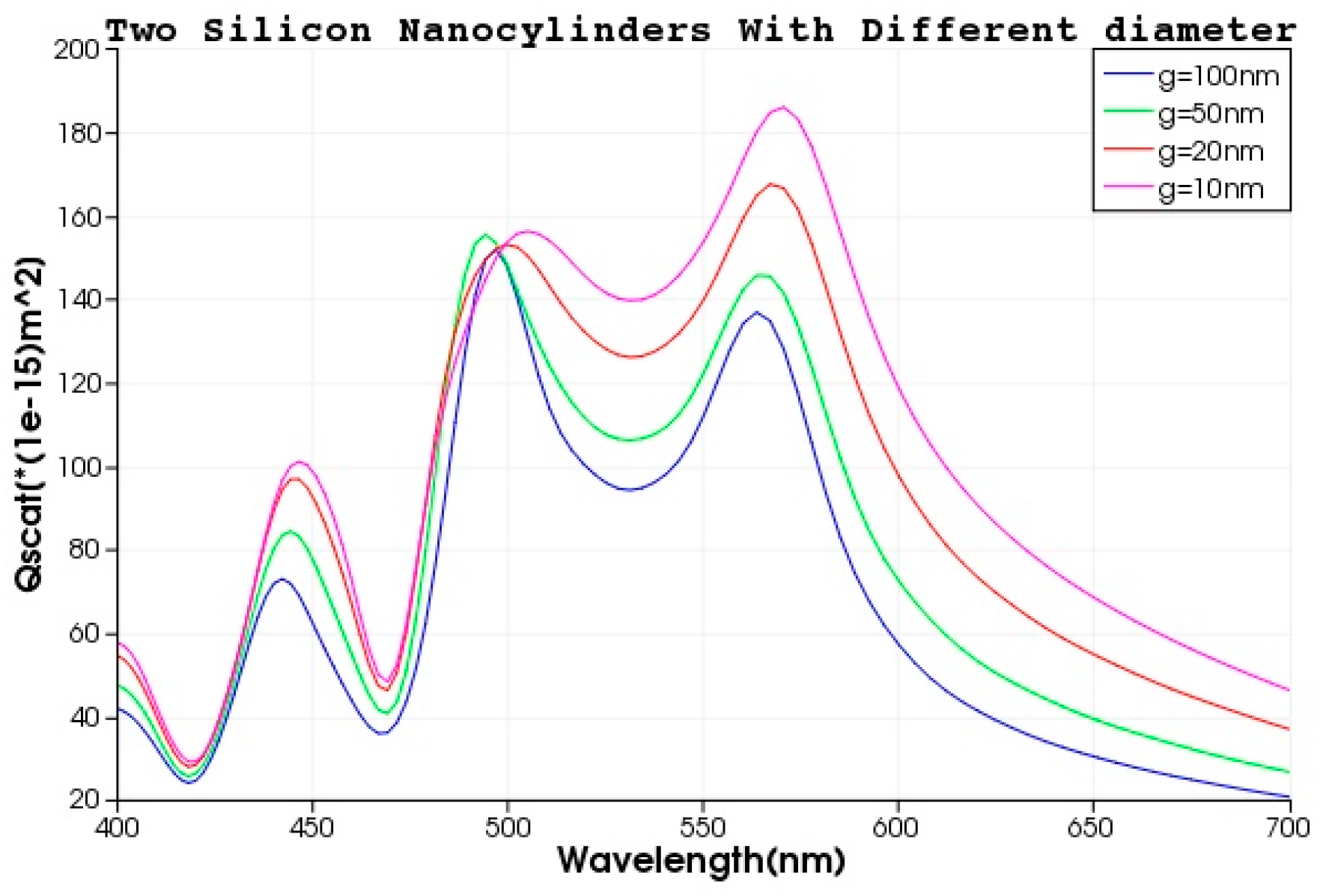
Next, we study the interaction between two identical silicon nanocylinders by changing the spacing g between two particles in Figure 6. When the gap g is comparable to the diameter 100 nm of nanocylinder, the scattering performance is similar to that of a single nanocylinder, except for the enhancement of scattering amplitude. The amplitude of electric dipole resonance is lower than that of magnetic dipole resonance, and both resonant modes are separated completely. As the spacing becomes smaller, the interaction between two nanocylinders becomes stronger, and a broadband scattering characteristic occurs.
In order to intuitively understand the effect of strong interaction of nanocylinders in close proximity on broadband scattering properties at the gap g = 10 nm, we study the electric and magnetic field distributions at the XOZ plane (y = 0). From the scattering cross-section curve, we select two positions: at λ = 444 nm and at λ = 499 nm, which have deviated from the electrical resonance at λ = 433 nm and the magnetic resonance at λ = 494 nm of a single nanocylinder.
From the electromagnetic field distribution in Figure 7, it can be seen that the strong electric field is concentrated on the gap between nanocylinders. In Figure 7a,b, at the electric field distribution indicates a roughly linear distribution, while the magnetic field shows an approximate node, implying the electric dipole resonant mode. It is obvious that the field distribution in dimeric nanocylinders demonstrates asymmetric features, which is attributed to the strong interaction between dimer. From Figure 7c,d, at the electric field, introduces a displacement current loop and the magnetic field indicates an antinode in each nanocylinder. These characteristics exhibit magnetic dipole resonance. It is interesting that by the enhancement of interaction with a decrease of gap, the scattering resonant bandwidth, including ED and MD, is broadened. The ED and MD resonances nearly merge with each other and form hybrid broadband resonant mode.
Next, the interaction of two different nanocyinders dimer is illustrated in detail by calculated scattering spectra in Figure 8. The scattering spectra were calculated with the two different nanocylinders at the unchanged gap width of 100 nm from Figure 8a–d. The diameter of one nanocylinder is 100 nm, and the diameter of the other nanocylinder is varying from 100 nm to 130 nm. In the case of Figure 8a, the scattering spectrum is similar to that of a single silicon nanocylinder, which indicates that the interaction between two nanocylinders is weak. As the diameter of the right nanocylinder in the double-nanocylinders-combination increases, the scattering amplitude of the electric resonance is decreased, and it shifts slightly closer to the mainly magnetic dipole resonance. When the diameter of the right nanocylinder is increased to 110 nm in Figure 8b, a newly emergent mode occurs. After carefully analysis, it results from the interaction of two nanocylinders. This new mode introduces a splitting phenomenon of magnetic dipole resonance. This mode can be named as “MD2”, and the original magnetic dipole resonance can be called as “MD1”. The splitting of “MD1” and “MD2” results from the magnetic-magnetic interaction in both of the nanocylinders. With the increase of diameter, the newly magnetic mode of “MD2” is redshift, but the resonant frequency of “MD1” is unchanged. Because of this splitting performance of magnetic resonance, the dimeric silicon nanocylinders shows a clear broadband scattering effect.
From Figure 8e–h, it is found that the resonant frequency of “MD2” is unchanged with the varying gap between two nanocylinders when the diameter of one nanocylinder is 100 nm and the diameter of other nanocylinder is 110 nm. The resonant amplitude of “MD2” is clearly increased, and it can be comparable to that of “MD1” in Figure 8h. Therefore, a broadband scattering resonance can be revealed by the coupling interaction effect between closely two nanocylinders. In order to further demonstrate the interaction, the scattering spectra were calculated as a function of the gap size in Figure 9 when the diameter of one nanocylinder is 100 nm and that of the other nanocylinder is 140 nm.
3.3. Scattering Characteristics of Three-Nanocylinders-Combination
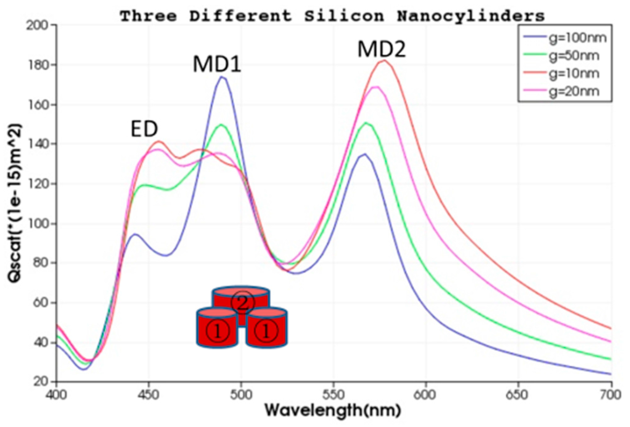
Next, we study the scattering characteristics and resonances of the three identical nanocylinders combination in Figure 10. By constructing trimeric silicon nanocylinders, more complex interaction can be introduced. Figure 10 shows the scattering performance of trimeric silicon nanocylinders with the gap from 100 nm to 10 nm. It is clear that the scattering performance is consistent with that of a single nanocylinder when g is 100 nm, showing a weaker interaction among three nanocylinders. As the spacing becomes smaller, the interaction becomes stronger and the obvious magnetic resonance splitting emerges as the gap is 50 nm. The newly “MD2” is more pronounced than that in the dimer. When g = 10 nm, the “MD1” seems to be disappeared, the “ED” and “MD2” modes become dominant scattering resonance. Because of the intense interaction, the splitting resonant modes result in a distinct dip, which is disadvantageous in broadband application. Furthermore, the scattering characteristics of three-different-nanocylinders-combination are studied in Figure 11. Two resonant peaks at short wavelength are close to each other and are mixed to form an electromagnetic resonant mixing mode with decreasing spacing. The magnetic resonance mode is becoming more and more significant when the spacing is decreased among three nanocylinders.
4. Influence of Substrate on Scattering Resonances
In fact, nanostructures can not be applied separately from substrate. For example, many optical elements can be efficiently applied when the electromagnetic field in nanoparticles are strongly coupled to substrate, hoping to absorb as much light as possible, such as photodiodes, solar cells, and so on. So, we place the nanoparticles on substrate to study the scattering characteristics. This interaction with a substrate must affect the electrical resonance, the magnetic resonance of the particles, and the interaction between them.
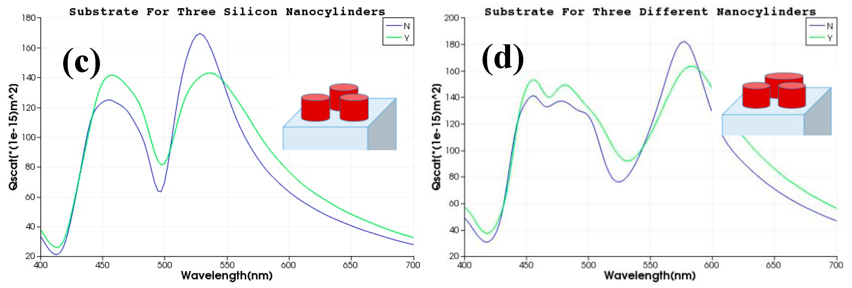
Figure 12a shows the scattering spectra of a single nanocylinder with and without substrate. “N”-curve indicates scattering without substrate, and “Y”-curve indicates scattering with a semi-infinite substrate of silica. It can be seen that the resonant frequency of ED and MD is slightly changed. The bandwidth of total scattering increases due to the presence of substrate. In addition, the electromagnetic field distributions are shown in Figure 12. The electric field in resonant mode is slightly extended into substrate, which result in enhancement of scattering bandwidth.
Furthermore, the effect of substrate on scattering resonances to double silicon nanocylinders and trimer nanocylinderts is shown in Figure 13. A clear performance is that the bandwidth of scattering resonances increases when the silicon nanostructure is located on the silica semi-infinite substrate. This indicates that the effect of resonant modes can be extended into the substrate. The substrate provides an additional height to the nanoparticles, so that a part of the electromagnetic resonance mode extends into the substrate, and the resonant modes are obviously widened.
5. Resonant Characteristics of Nanocylinder-Periodic-Array
Next, in order to further understand the effect of the interaction between nanoparticles, we have attempted to study the electromagnetic dipole resonance of the nanocylinder-periodic-array. Firstly, we designed a single nanocylinder periodic array without substrate, which is shown in inset of Figure 14. The period “T” of nanostructure is 400 nm along both x-direction and y-direction. The height and diameter of nanocylinder are 100 nm. From Figure 14, it can be seen that the resonant frequency of ED and MD is unchanged when compared with that for a single nanocylinder due to the negligible interaction between nanocylinders.
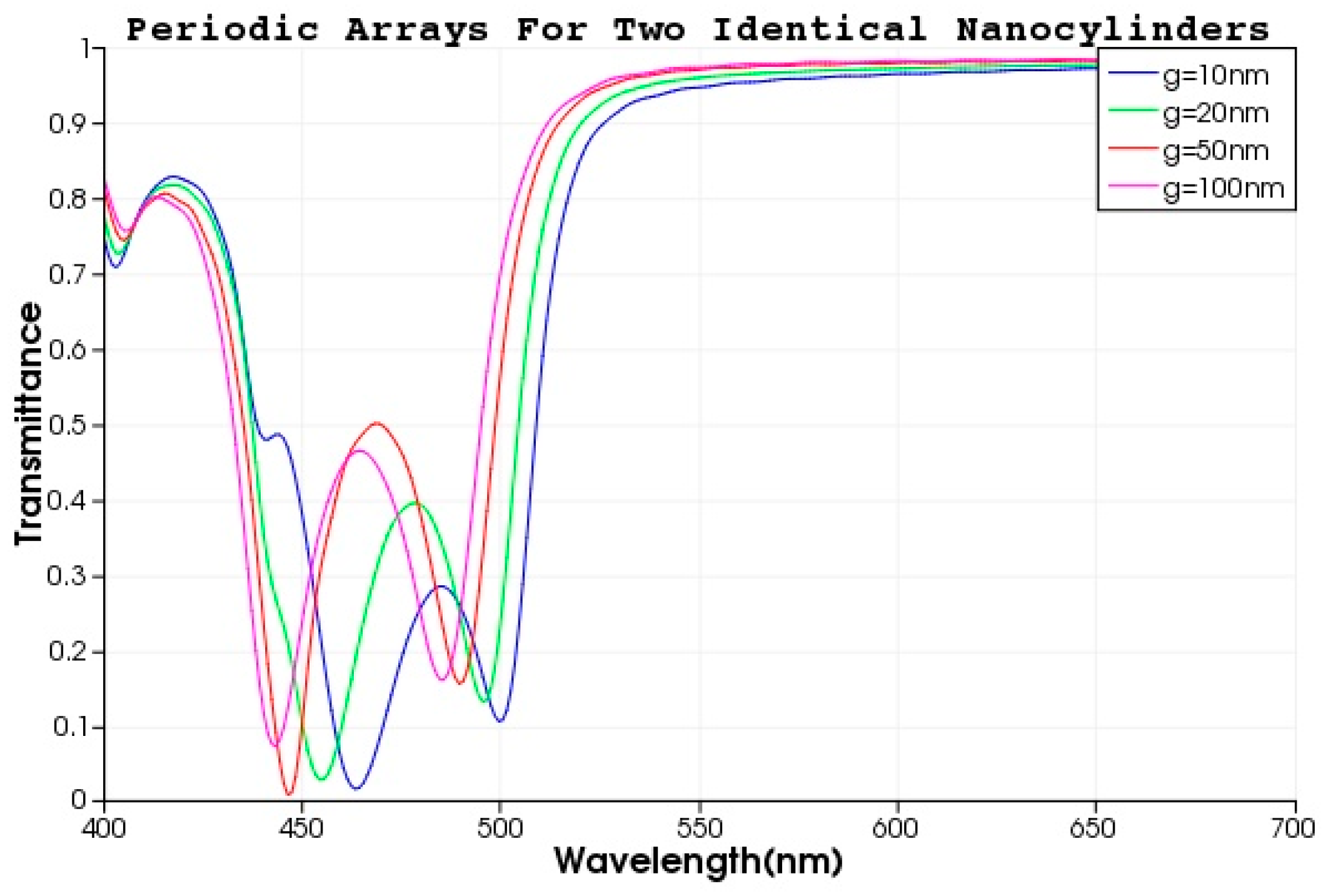
In Figure 15, the transmission characteristic of double-nanocylinders periodic array is indicated with varying gap from 100 nm to 10 nm. When compared with Figure 14 for a single nanocylinder periodic structure, the transmission for both resonances is smaller, which indicates that the resonant effect of double nanocylinders is enhanced due to the interaction in periodic array in Figure 15. It is interesting that when the gap is decreased to 10 nm, a newly electric resonant mode emerges, which is shown by a red arrow in Figure 15. This newly emergent mode can be attributed to electric-electric interaction. Therefore, when the resonance characteristics of a periodic array are studied, we should not only take into account the interaction between particles in each period, but also take into account the interaction between periods.
6. Summary
The resonant characteristics of dielectric nanocylinders in visible spectrum is systematically studied. When decreasing the spacing between nanocylinders, the interaction between the particles changes from weak to strong. Magnetic field in the nanocylinders in dimer and trimer affect with each other, leading to the introduction of a new magnetic resonance mode. The compact nanocylinders structures combination presents a broadband scattering when compared with a single silicon nanocylinder. The effect of substrate on resonant scattering performance is demonstrated, which results in the enhancement of bandwidth of scattering. The resonant scattering characteristics in periodic array structure are also revealed. These results can be applied to develop various broadband resonant devices.
Acknowledgments
The authors acknowledge the support from National Key R&D Program of China (Grant No. 2016YFF0100505), Natural Science Foundation of Zhejiang Province (LY17F050009, LQ15F050004), National Natural Science Foundation of China (NSFC) (No. 61405182, No. 61505192).
Author Contributions
The contributions of Bo Fang are writing text and part of simulation. Xufeng Jing putted forward idea of this paper. The contributions of Qiufeng Ye, Jinhui Cai and Pengwei Zhou are theoretical analysis about formula and numerical results.
Conflicts of Interest
The authors declare no conflict of interest.
References
- Sun, D.; Wang, M.; Huang, Y.; Zhou, Y.; Qi, M.; Jiang, M.; Ren, Z. Enhanced spatial terahertz modulation based on graphene metamaterial. Chin. Opt. Lett. 2017, 15, 051603. [Google Scholar]
- Sun, Q.; Wang, S.; Liu, H.; Zhu, S. Highly efficient mid-infrared metasurface based on metallic rods and plate. Chin. Opt. Lett. 2016, 14, 051101. [Google Scholar]
- Luigi, B.; Khan, K.; Liu, Q.; Lin, M.; Wang, Q.; Ouyang, Z. Tunable narrowband antireflection optical filter with a metasurface. Photonics Res. 2017, 5, 500–506. [Google Scholar]
- Cao, T.; Li, Y.; Zhang, X.; Zou, Y. Theoretical study of tunable chirality from graphene integrated achiral metasurfaces. Photonics Res. 2017, 5, 441–449. [Google Scholar] [CrossRef]
- Kwon, M.K.; Kim, J.Y.; Kim, B.H.; Park, I.K.; Cho, C.Y.; Byeon, C.C.; Park, S.J. Surface-plasmon-enhanced light-emitting diodes. Adv. Mater. 2008, 20, 1253–1257. [Google Scholar] [CrossRef]
- Atwater, H.A.; Polman, A. Plasmonics for improved photovoltaic devices. Nat. Mater. 2010, 9, 205–213. [Google Scholar] [CrossRef] [PubMed]
- Ferry, V.E.; Verschuuren, M.A.; Li, H.B.T.; Verhagen, E.; Walters, R.H.; Schropp, R.E.I.; Atwater, H.A.; Polman, A. Light trapping in ultrathin plasmonic solar cells. Opt. Express 2010, 18, A237–A245. [Google Scholar] [CrossRef] [PubMed]
- Evlyukhin, A.B.; Reinhardt, C.; Seidel, A.; Luk’yanchuck, B.S.; Chichkov, B.N. Optical response features of Si-nanoparticle arrays. Phys. Rev. B 2010, 82, 045404. [Google Scholar] [CrossRef]
- Kuznetsov, A.I.; Miroschnichenko, A.E.; Fu, Y.H.; Zhang, J.B.; Luk’yanchuk, B. Magnetic light. Sci. Rep. 2012, 2, 492. [Google Scholar] [CrossRef] [PubMed]
- Fan, P.; Huang, K.C.Y.; Cao, L.; Brongersma, M.L. Redesigning photodetector electrodes as an optical antenna. Nano Lett. 2013, 13, 392–396. [Google Scholar] [CrossRef] [PubMed]
- Schuller, J.A.; Barnard, E.S.; Cai, W.; Jun, Y.C.; White, J.S.; Brongersma, M.L. Plasmonics for extreme light concentration and manipulation. Nat. Mater. 2010, 9, 193–204. [Google Scholar] [CrossRef] [PubMed]
- Tian, X.; Li, Z. Visible-near infrared ultra-broadband polarization-independent metamaterial perfect absorber involving phase-change materials. Photonics Res. 2016, 4, 146–152. [Google Scholar] [CrossRef]
- Fu, Y.H.; Kuznetsov, A.I.; Miroschnichenko, A.E.; Yu, Y.F.; Luk’yanchuk, B. Directional visible light scattering by silicon nanoparticles. Nat. Commun. 2013, 4, 1527. [Google Scholar] [CrossRef] [PubMed]
- Bu, T.; Chen, K.; Liu, H.; Liu, J.; Zhi, H.; Zhuang, S. Location-dependent metamaterials in terahertz range for reconfiguration purposes. Photonics Res. 2016, 4, 122–125. [Google Scholar] [CrossRef]
- Zhao, Q.; Zhou, J.; Zhang, F.; Lippens, D. Mie resonance-based dielectric metamaterials. Mater. Today 2009, 12, 60–69. [Google Scholar] [CrossRef]
- Ginn, J.C.; Brener, I.; Peters, D.W.; Wendt, J.R.; Stevens, J.O.; Hines, P.F.; Basilio, L.I.; Warne, L.K.; Ihlefeld, J.F.; Clem, P.G.; et al. Realizing optical magnetism from dielectric metamaterials. Phys. Rev. Lett. 2012, 108, 097402. [Google Scholar] [CrossRef] [PubMed]
- Bakker, R.M.; Permyakov, D.; Yu, Y.F.; Markovich, D.; Paniagua-Domínguez, R.; Gonzaga, L.; Samusev, A.; Kivshar, Y.; Luk’yanchuk, B.; Kuznetsov, A.I. Magnetic and electric hotspots with silicon nanodimers. Nano Lett. 2015, 15, 2137–2142. [Google Scholar] [CrossRef] [PubMed]
- Evlyukhin, A.B.; Novikov, S.M.; Zywietz, U.; Eriksen, R.L.; Reinhardt, C.; Bozhevolnyi, S.I.; Chichkov, B.N. Demonstration of Magnetic Dipole Resonances of Dielectric Nanospheres in the Visible Region. Nano Lett. 2012, 12, 3749–3755. [Google Scholar] [CrossRef] [PubMed]
- Person, S.; Jain, M.; Lapin, Z.; Saenz, J.J.; Wicks, G.; Novotny, L. Demonstration of Zero Optical Backscattering from Single Nanoparticles. Nano Lett. 2013, 13, 1806–1809. [Google Scholar] [CrossRef] [PubMed]
- Miroshnichenko, A.E.; Kivshar, Y.S. Fano Resonances in All Dielectric Oligomers. Nano Lett. 2012, 12, 6459–6463. [Google Scholar] [CrossRef] [PubMed]
- Chong, K.E.; Hopkins, B.; Staude, I.; Miroshnichenko, A.E.; Dominguez, J.; Decker, M.; Neshev, D.N.; Brener, I.; Kivshar, Y.S. Observation of Fano Resonances in All-Dielectric Nanoparticle Oligomers. Small 2014, 10, 1985–1990. [Google Scholar] [CrossRef] [PubMed]
- Albella, P.; Poyli, M.A.; Schmidt, M.K.; Maier, S.A.; Moreno, F.; Saenz, J.J.; Aizpurua, J. Low-Loss Electric and Magnetic Field-Enhanced Spectroscopy with Subwavelength Silicon Dimers. J. Phys. Chem. C 2013, 117, 13573–13584. [Google Scholar] [CrossRef]
- Albella, P.; Alcaraz de la Osa, R.; Moreno, F.; Maier, S.A. Electric and Magnetic Field Enhancement with Ultralow Heat Radiation Dielectric Nanoantennas: Considerations for Surface Enhanced Spectroscopies. ACS Photonics 2014, 1, 524–529. [Google Scholar] [CrossRef]
- Wang, C.; Jia, Z.Y.; Zhang, K.; Zhou, Y.; Fan, R.H.; Xiong, X.; Peng, R.W. Broadband optical scattering in coupled silicon nanocylinders. J. Appl. Phys. 2014, 115, 244312. [Google Scholar] [CrossRef]
- Boudarham, G.; Abdeddaim, R.; Bonod, N. Enhancing the magnetic field intensity with a dielectric gap antenna. Appl. Phys. Lett. 2014, 104, 021117. [Google Scholar] [CrossRef]
- Schmidt, M.K.; Esteban, R.; Saenz, J.J.; Suárez-Lacalle, I.; Mackowski, S.; Aizpurua, J. Dielectric antennas—A suitable platform for controlling magnetic dipolar emission. Opt. Express 2012, 20, 13636–13650. [Google Scholar] [CrossRef] [PubMed]
- Shi, L.; Tuzer, T.U.; Fenollosa, R.; Meseguer, F. A new dielectric metamaterial building block with a strong magnetic response in the sub-1.5-micrometer region: Silicon colloid nanocavities. Adv. Mater. 2012, 24, 5934–5938. [Google Scholar] [CrossRef] [PubMed]
- Yu, N.; Capasso, F. Flat optics with designer metasurfaces. Nat. Mater. 2014, 13, 139–150. [Google Scholar] [CrossRef] [PubMed]
- Rolly, B.; Stout, B.; Bonod, N. Boosting the directivity of optical antennas with magnetic and electric dipolar resonant particles. Opt. Express 2012, 20, 20376–20386. [Google Scholar] [CrossRef] [PubMed]
- Schmidt, M.K.; Aizpurua, J.; Zambrana-Puyalto, X.; Vidal, X.; Molina-Terriza, G.; Saenz, J.J. Isotropically polarized speckle patterns. Phys. Rev. Lett. 2015, 114, 113902. [Google Scholar] [CrossRef] [PubMed]
- Palik, E.D. Handbook of Optical Constants of Solids; Academic Press: New York, NY, USA, 1985; Volume 1, p. 555. [Google Scholar]
- Mulholland, G.W.; Bohren, C.F.; Fuller, K.A. Light scattering by agglomerates: Coupled electric and magnetic dipole method. Langmuir 1994, 10, 2533–2546. [Google Scholar] [CrossRef]
Figure 1.
(a) The schematic of nanocylinder, the direction of the red arrow indicates the direction of the displacement current, and the incident wave is normally incidence; and, (b) Interaction between nanocylinders with and without substrate.
Figure 1.
(a) The schematic of nanocylinder, the direction of the red arrow indicates the direction of the displacement current, and the incident wave is normally incidence; and, (b) Interaction between nanocylinders with and without substrate.
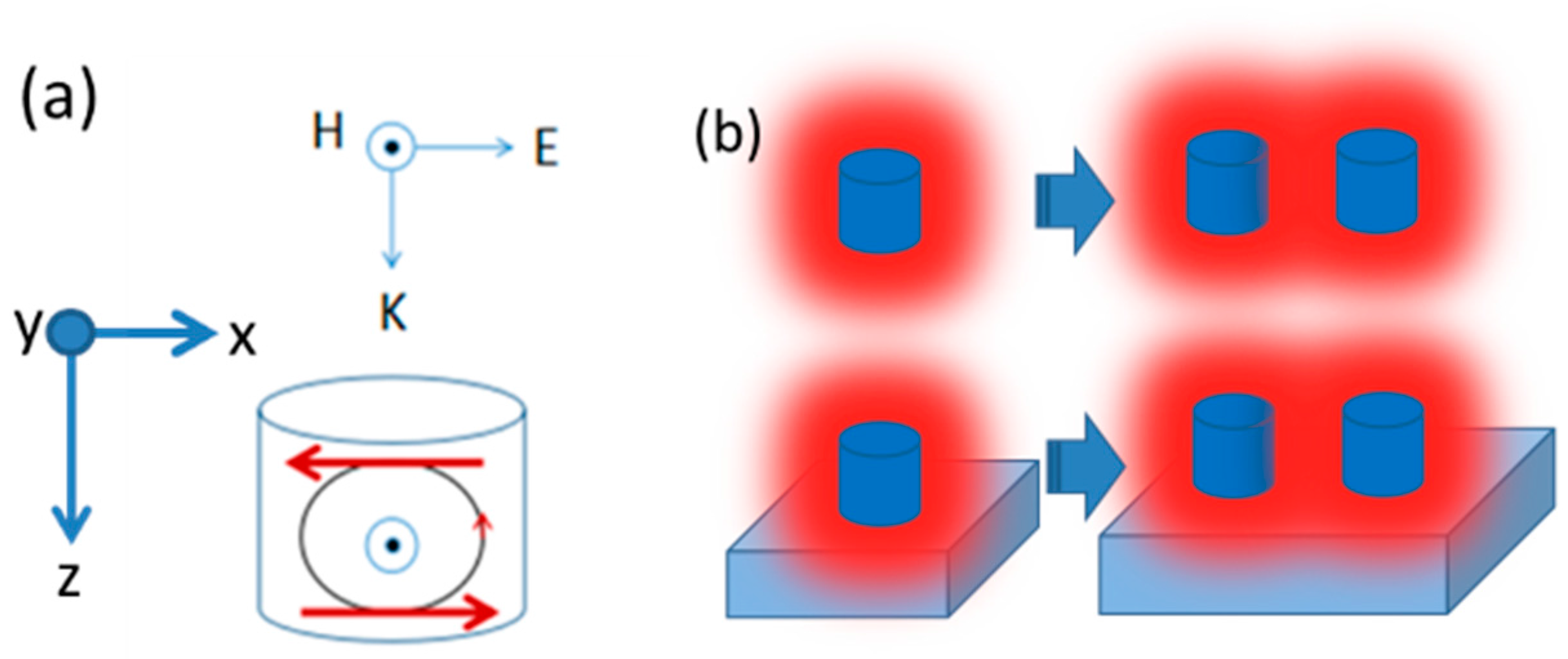
Figure 2.
Scattering cross-section of a single silicon nanocylinder.
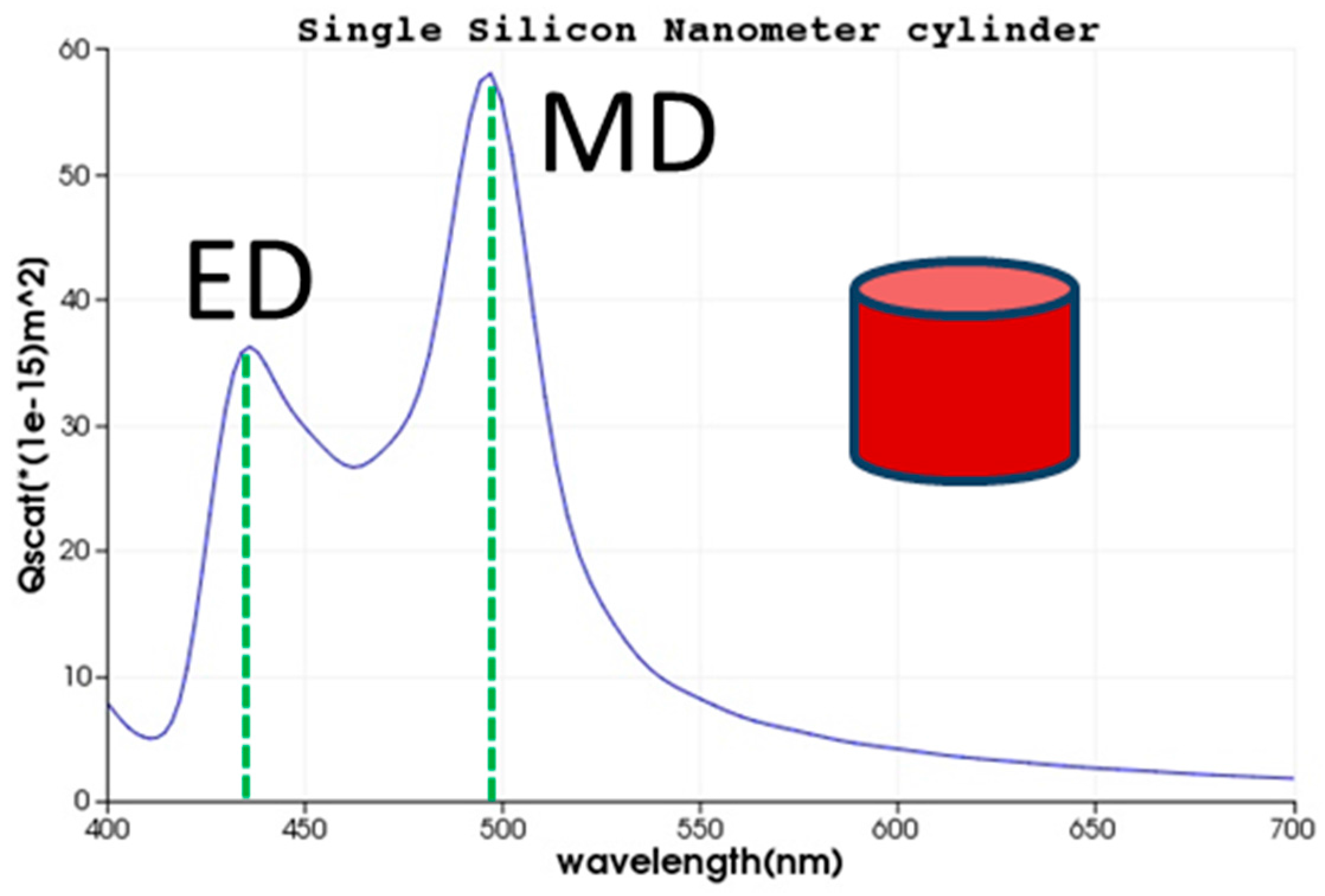
Figure 3.
The electric field vector distribution of the XOZ cross-section at the center of nanocylinder. (a) at ; (b) at .
Figure 3.
The electric field vector distribution of the XOZ cross-section at the center of nanocylinder. (a) at ; (b) at .

Figure 4.
(a) The electric field distribution and (b) the magnetic field distribution at at XOZ plane through the center of the nanocylinder, respectively; (c) The electric field distribution and (d) the magnetic field distribution at at XOZ plane through the center of the nanocylinder, respectively.

Figure 5.
Scattering spectra of a single silicon nanocylinder with (a) various radius R and (b) various height of nanocylinder in air.
Figure 5.
Scattering spectra of a single silicon nanocylinder with (a) various radius R and (b) various height of nanocylinder in air.
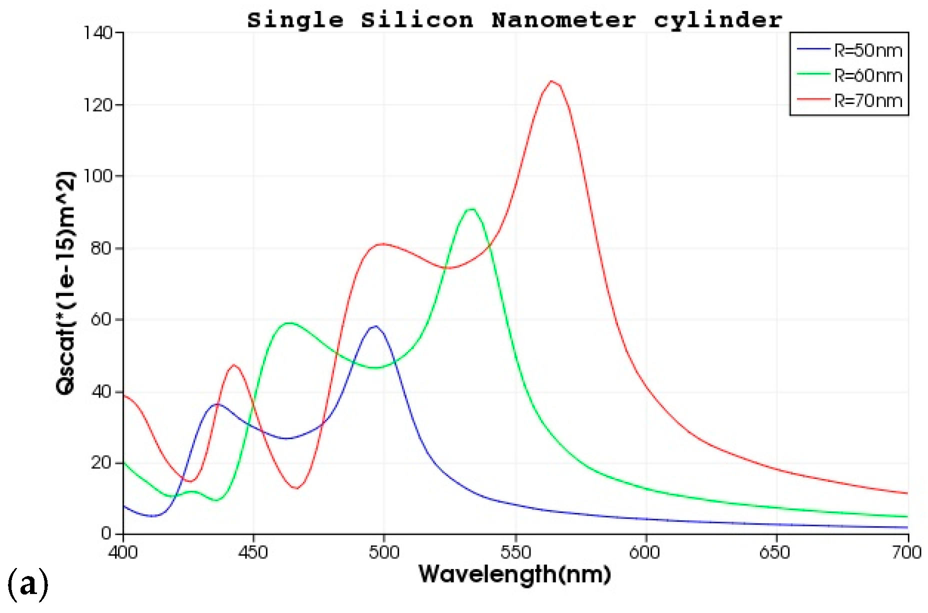

Figure 6.
Scattering spectra of double-nanocylinders-combination with the decreasing spacing from 100 nm in air. g represents the spacing between two nanocylinders. The diameter and height are 100 nm.
Figure 6.
Scattering spectra of double-nanocylinders-combination with the decreasing spacing from 100 nm in air. g represents the spacing between two nanocylinders. The diameter and height are 100 nm.
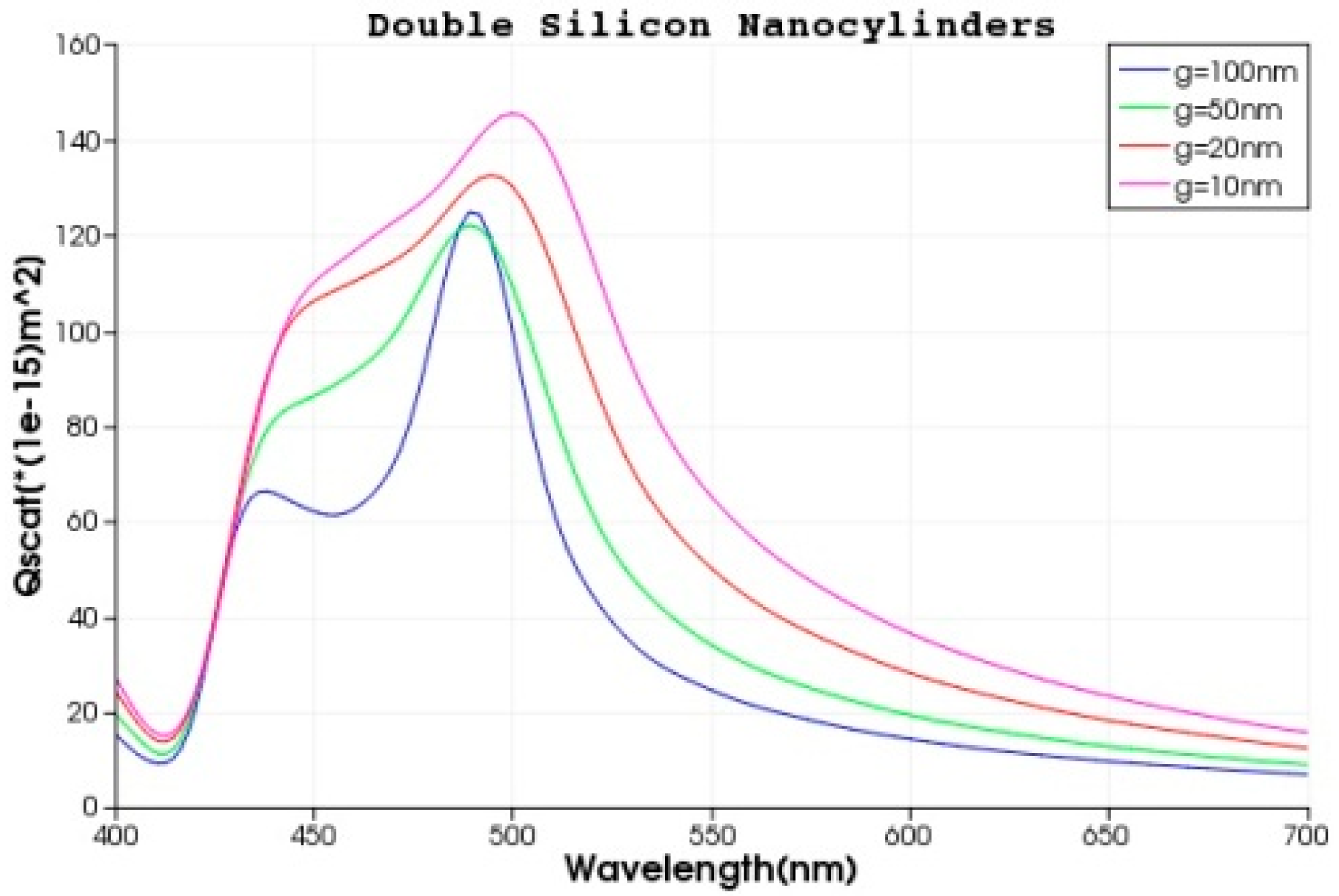
Figure 7.
The intensity distributions of electric field and magnetic field of the dimer with gap g = 10 nm at (a,b) and (c,d) , respectively, at XOZ plane.
Figure 7.
The intensity distributions of electric field and magnetic field of the dimer with gap g = 10 nm at (a,b) and (c,d) , respectively, at XOZ plane.
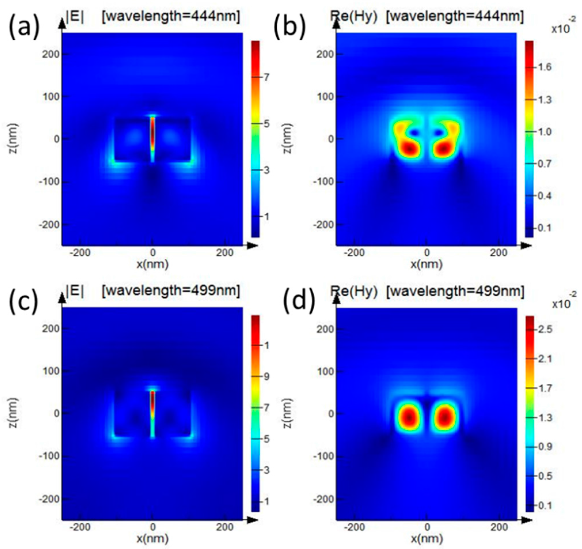
Figure 8.
Calculated scattering spectra of dimers. (a–d) the diameter of left nanocylinder is unchanged, the nanocylinder gaps are unchanged with g = 100 nm, and the diameter of the right nanocylinder is changed from (a) 100 nm to (d) 130 nm. (e–h) nanocylinder gaps varying from 100 nm to 10 nm, Both silicon nanocylinders are different with the diameter 100 nm of left nanocylinder and the diameter 110 nm of right nanocylinder.
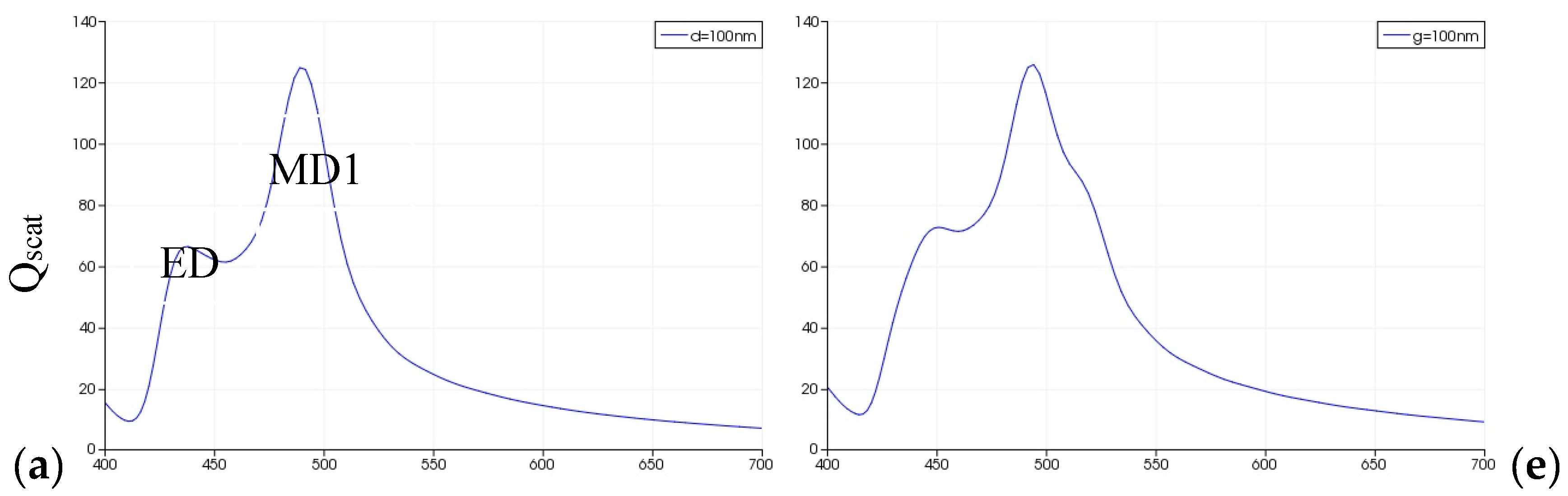
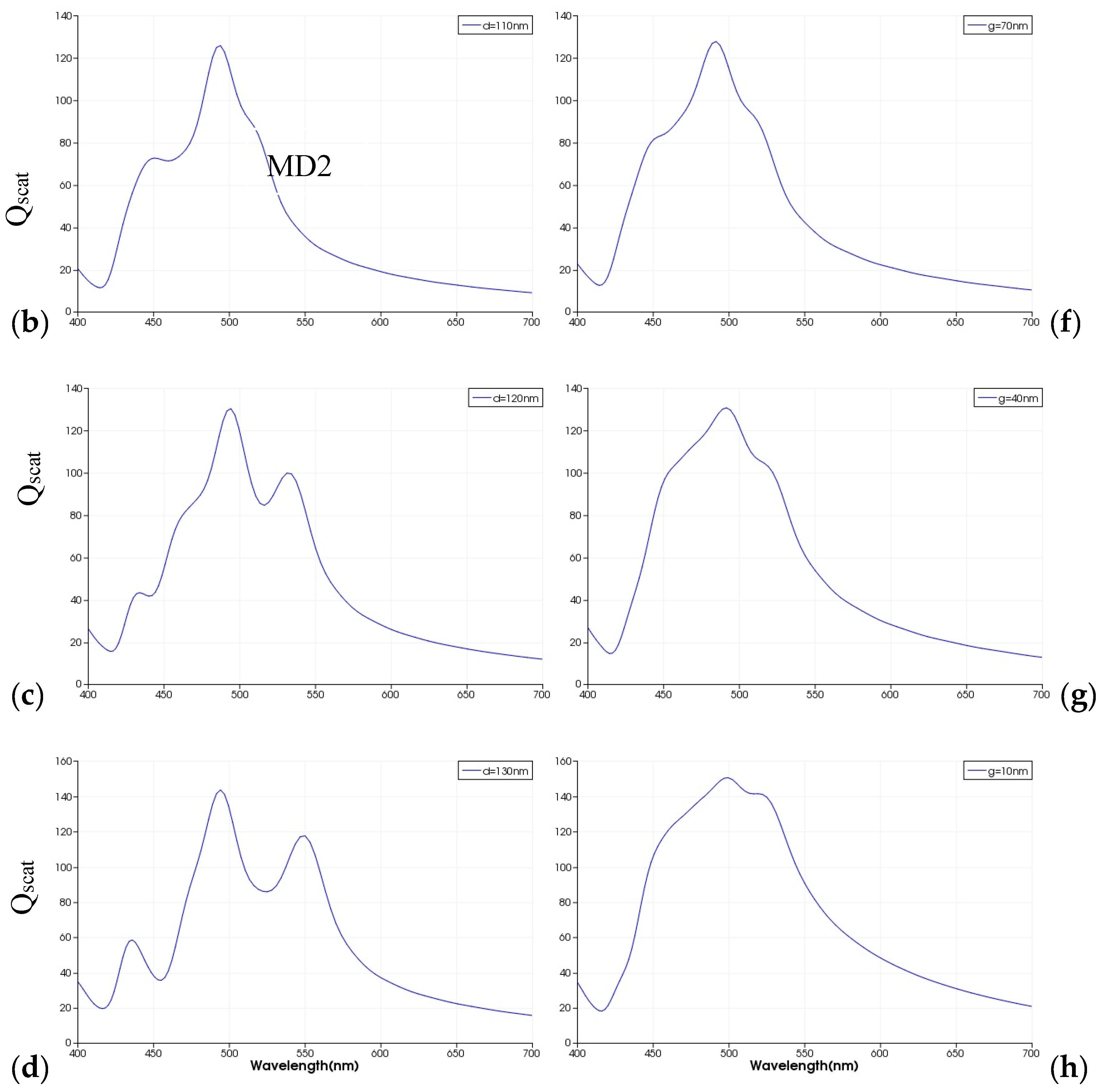
Figure 9.
Scattering spectra of two-different-nanocylinders-combination with the decreasing spacing from 100 nm in air. The height of cylinders is still 100 nm, while the diameter of the left nanocylinder is 100 nm, and the diameter of the right nanocylinder is 140 nm.
Figure 9.
Scattering spectra of two-different-nanocylinders-combination with the decreasing spacing from 100 nm in air. The height of cylinders is still 100 nm, while the diameter of the left nanocylinder is 100 nm, and the diameter of the right nanocylinder is 140 nm.

Figure 10.
Scattering of three- identical-nanocylinders-combination with decreasing spacing from 100 nm in air. The height and diameter of three same nanocylinders are both 100 nm.
Figure 10.
Scattering of three- identical-nanocylinders-combination with decreasing spacing from 100 nm in air. The height and diameter of three same nanocylinders are both 100 nm.
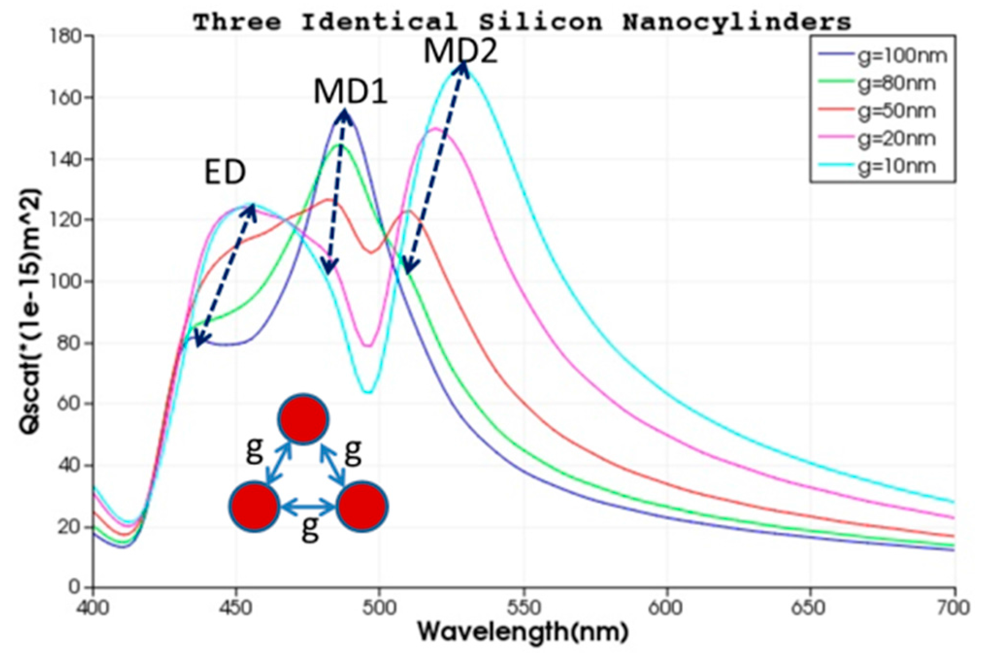
Figure 11.
Scattering spectrum of three-different-nanocylinders-combination with decreasing spacing from 100 nm in air. The size of two different kinds of cylinders are: ① the height and diameter are 100 nm; and, ② the height is 100 nm and the diameter is 140 nm.
Figure 11.
Scattering spectrum of three-different-nanocylinders-combination with decreasing spacing from 100 nm in air. The size of two different kinds of cylinders are: ① the height and diameter are 100 nm; and, ② the height is 100 nm and the diameter is 140 nm.

Figure 12.
(a) Scattering cross-section of a single silicon nanocylinder with a height of 100 nm and a diameter of 100 nm on a semi-infinite substrate of silica. The N-curve describes the scattering spectrum when there is no substrate, and the Y-curve describes the scattering spectrum of the structure on the substrate; (b–e) The electromagnetic field of the single-silicon-nanocylider on a semi-infinite substrate of silica at and ; (b,d) The electric field distribution of the longitudinal section along the XOZ plane through the center of the nanocylinders; (c,e) The magnetic field distribution of the longitudinal section along the XOZ plane through the center of the nanocylinders.
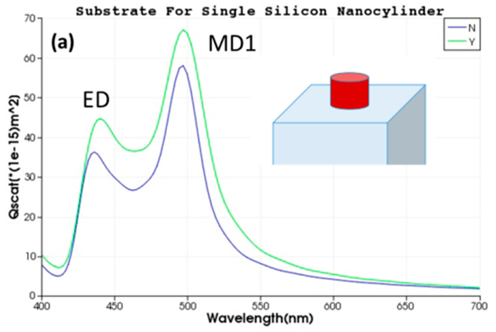
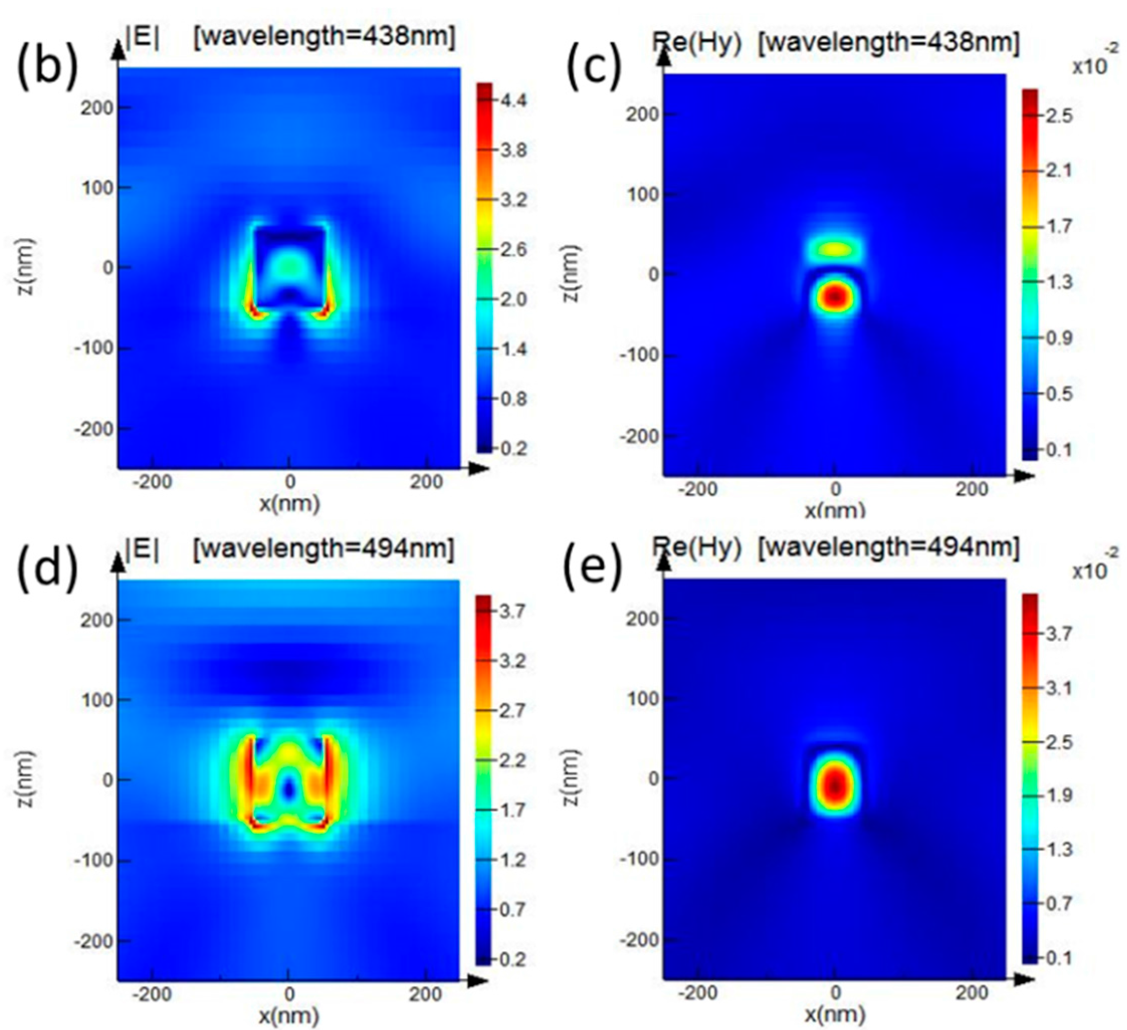
Figure 13.
Scattering cross section for (a) the double-nanocylinders-combination; (b) two-different-nanocylinders-combination; and, (c) three-identical-nanocylinders-combination; (d) three-different-nanocylinders-combination on a semi-infinite substrate of silica. The dimensions of the nanocylinders: ① the height of 100 nm and the diameter of 100 nm and ② the height of 100 nm and the diameter of 140 nm.
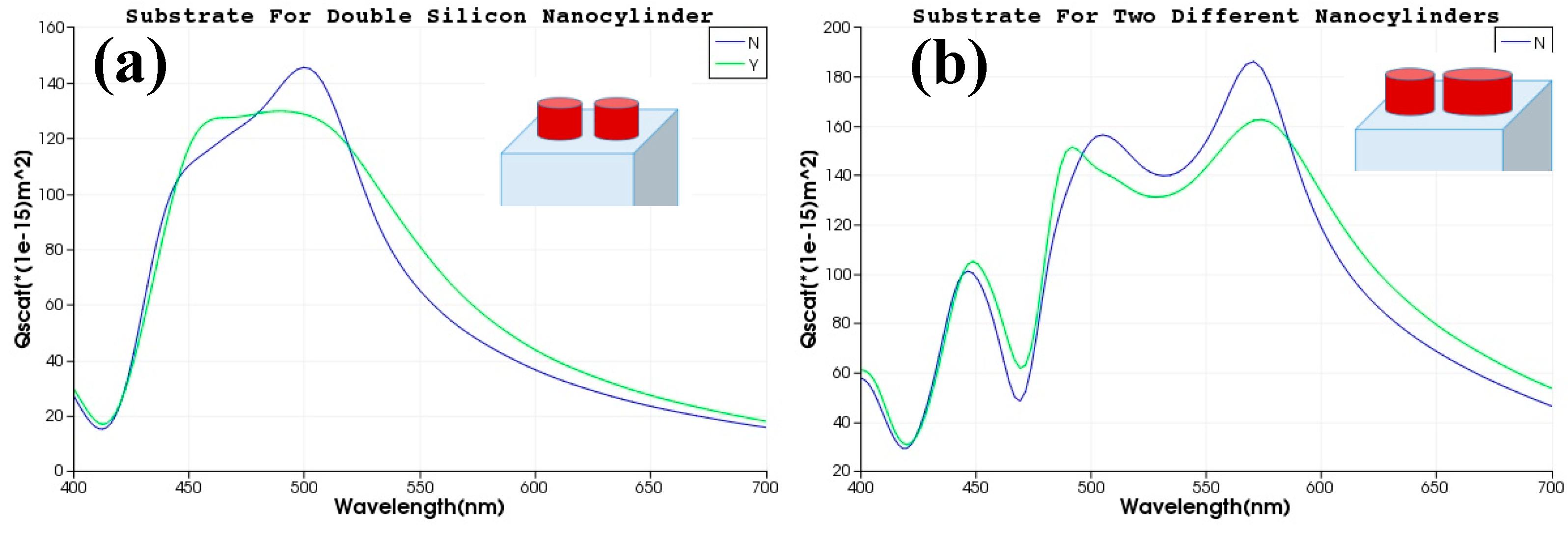

Figure 14.
The transmission and reflection of the single nanocylinder periodic array without substrate.
Figure 14.
The transmission and reflection of the single nanocylinder periodic array without substrate.
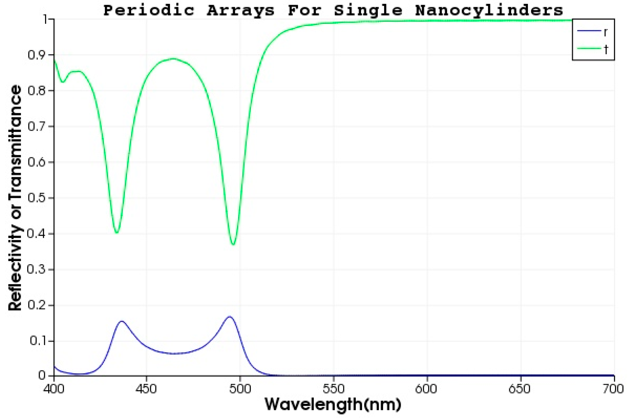
Figure 15.
The transmission of double-nanocylinders-periodic-array, and one period in array is consisted of two silicon nanocylinders. The height and diameter of both nanocylinders are 100 nm. The period T of array is 400 nm.
Figure 15.
The transmission of double-nanocylinders-periodic-array, and one period in array is consisted of two silicon nanocylinders. The height and diameter of both nanocylinders are 100 nm. The period T of array is 400 nm.
© 2018 by the authors. Licensee MDPI, Basel, Switzerland. This article is an open access article distributed under the terms and conditions of the Creative Commons Attribution (CC BY) license (http://creativecommons.org/licenses/by/4.0/).
Share and Cite
MDPI and ACS Style
Fang, B.; Jing, X.; Ye, Q.; Cai, J.; Zhou, P. Broadband Electromagnetic Dipole Resonance by the Coupling Effect of Multiple Dielectric Nanocylinders. Appl. Sci. 2018, 8, 60. https://doi.org/10.3390/app8010060
AMA Style
Fang B, Jing X, Ye Q, Cai J, Zhou P. Broadband Electromagnetic Dipole Resonance by the Coupling Effect of Multiple Dielectric Nanocylinders. Applied Sciences. 2018; 8(1):60. https://doi.org/10.3390/app8010060
Chicago/Turabian StyleFang, Bo, Xufeng Jing, Qiufeng Ye, Jinhui Cai, and Pengwei Zhou. 2018. "Broadband Electromagnetic Dipole Resonance by the Coupling Effect of Multiple Dielectric Nanocylinders" Applied Sciences 8, no. 1: 60. https://doi.org/10.3390/app8010060
Note that from the first issue of 2016, this journal uses article numbers instead of page numbers. See further details here.