Article

Bloch Surface Wave Photonic Device Fabricated by Femtosecond Laser Polymerisation Technique

by
Ksenia A. Abrashitova
1,2,
Dmitry N. Gulkin
1,
Kirill R. Safronov
1,
Natalia G. Kokareva
1,
Ilya M. Antropov
1,
Vladimir O. Bessonov
1,3,* and
Andrey A. Fedyanin
1
1
Faculty of Physics, Lomonosov Moscow State University, Moscow 119991, Russia
2
Institute of Physics, Mathematics and Informational Technologies, Center for Functionalized Magnetic Materials (FunMagMa), Immanuel Kant Baltic Federal University, Kaliningrad 236041, Russia
3
Frumkin Institute of Physical Chemistry and Electrochemistry, Russian Academy of Sciences, Moscow 119071, Russia
*
Author to whom correspondence should be addressed.
Appl. Sci. 2018, 8(1), 63; https://doi.org/10.3390/app8010063
Submission received: 30 November 2017 / Revised: 29 December 2017 / Accepted: 30 December 2017 / Published: 4 January 2018
(This article belongs to the Special Issue Surface Waves on Planar Photonic Crystals)

Abstract

:
We applied femtosecond laser polymerisation technique to fabricate a novel Bloch surface wave integrated photonic device with a compact coupling scheme. The device consisted of a waveguide, coupling and decoupling gratings and focusing and defocusing triangles. We manufactured an array of devices with varying geometrical parameters of waveguide. Excitation and propagation of Bloch surface wave waveguide modes were studied by direct and back focal plane imaging. The obtained results prove that the maskless and flexible femtosecond laser polymerisation technique may be applied for fabrication of Bloch-surface-wave based integrated photonics.

1. Introduction

Integrated photonics is a branch of optics that is dedicated to the development of miniature devices on a single chip that generate, guide, modulate and detect optical signals. The approaches that utilise surface electromagnetic waves (SEWs) seem to be advantageous compared to the bulky waveguide mode approaches. SEW-supporting optical components are intrinsically planar and thus compatible with well-developed lithographic techniques. Subwavelength confinement of SEW amplifies light–matter interaction, which enhances refractive index sensitivity as well as switching efficiency of SEW-based photonic devices.
The most widely-studied type of SEWs are surface plasmon polaritons (SPPs). Unfortunately, SPPs suffer from severe shortcomings that strongly limit the performance of SPP-based devices: sensors and elements of integrated optics. SPPs propagating on a metal surface are strongly attenuated due to Ohmic losses. Plasmonic waveguide performance is always a trade-off between field confinement and propagation distance: for waveguides with high confinement, SPP propagation distances are only dozens of microns (channel plasmon–polaritons), while millimetre range propagation distances lead to a very weak confinement, much larger then the incident wavelength (long-range surface plasmon–polariton waveguides) [1]. Moreover, the SPP dispersion law is strictly defined by the properties of several metals.
Bloch surface waves (BSWs) are SEWs confined on an interface between one-dimensional (1D) photonic crystal and dielectric medium [2,3]. In contrast to SPP, BSW modes are supported by fully dielectric structures, which relieves them from Ohmic losses. The propagation length of BSWs was demonstrated to be in the millimetre range at telecommunication wavelengths [4]. The BSW dispersion law may be arbitrarily tuned by changing parameters and material of one-dimensional photonic crystal [4]. BSWs may be excited in a wide wavelength range from IR to UV [5]. They have received much attention in recent years, mostly because of their potential in sensing. BSW-based gas, protein, antibody, glucose, and protease detectors as well as BSW-induced enhanced Raman scattering have been successfully demonstrated [6,7,8,9,10,11,12,13]. Different effects in the presence of BSWs have been experimentally observed including the enhancement of fluorescence [14] and magneto-optical effects [15], giant Goos–Hänchen effect [16], and BSW-induced radiation forces [17,18].
In Reference "Guided Bloch surface waves on ultrathin polymeric ridges" [19], it was demonstrated that BSW may be confined and guided in thin polymeric stripes. This pioneering work proved that BSW propagation may be easily managed by simple lithographic nanostructuring of the top layer of the photonic crystal. Since then, a wide spectrum of complex photonic devices has been demonstrated, including lenses [20], a prism [21], square and round gratings [22,23], a subwavelength focusing device [24], a polarisation-sensitive beam splitter [25], and a disk resonator [26]. However, the basic and the most important element of integrated photonics—waveguide—remains not fully studied. There are a number of works where the BSW propagation in thin dielectric waveguides has been studied [27,28,29,30]. The excitation of BSW was achieved in either Kretschmann configuration, or by tapered fiber. However, these bulky methods of coupling the BSW with incident radiation are not compatible with ready for use devices. Practical applications demand more compact diffraction grating excitation schemes, which can be easily integrated into the photonic chip, optimized, and aligned in the flat optical scheme. Although there are a number of works where diffraction grating was successfully applied to excite the BSW on the surface of the photonic crystal [22,23], there is no experimental proof of the possibility of the BSW waveguide mode coupling to incident radiation by the diffraction grating excitation method.
It is also important to carefully choose the structuring method due to sensitivity of the BSW excitation and propagation to geometrical parameters of the BSW-supporting structures. The femtosecond laser polymerisation technique (or two-photon polymerisation technique 2PP) is an advanced lithographic technique that is based on nonlinear absorption phenomena and provides sub-100 nm resolution [31,32]. This method has found successful applications in microfluidics, tissue engineering, micro-optics (including X-ray optics [33]), micromechanics and photonics [34]. 2PP provides precise control of geometrical shape and allows for fabricating several nanostructures with slightly deviating geometrical parameters on a single substrate in one exposition procedure [35].
In this paper, we proposed a femtosecond laser polymerisation technique for nanofabrication of novel BSW-supporting photonics devices. A compact excitation scheme provides full compatibility with integrated optics technology. The propagation of the BSW in the device was studied both experimentally and numerically. Obtained experimental results prove the applicability of 2PP for the BSW-based integrated photonics as well as the applicability of diffraction grating for excitation of the BSW waveguide modes.

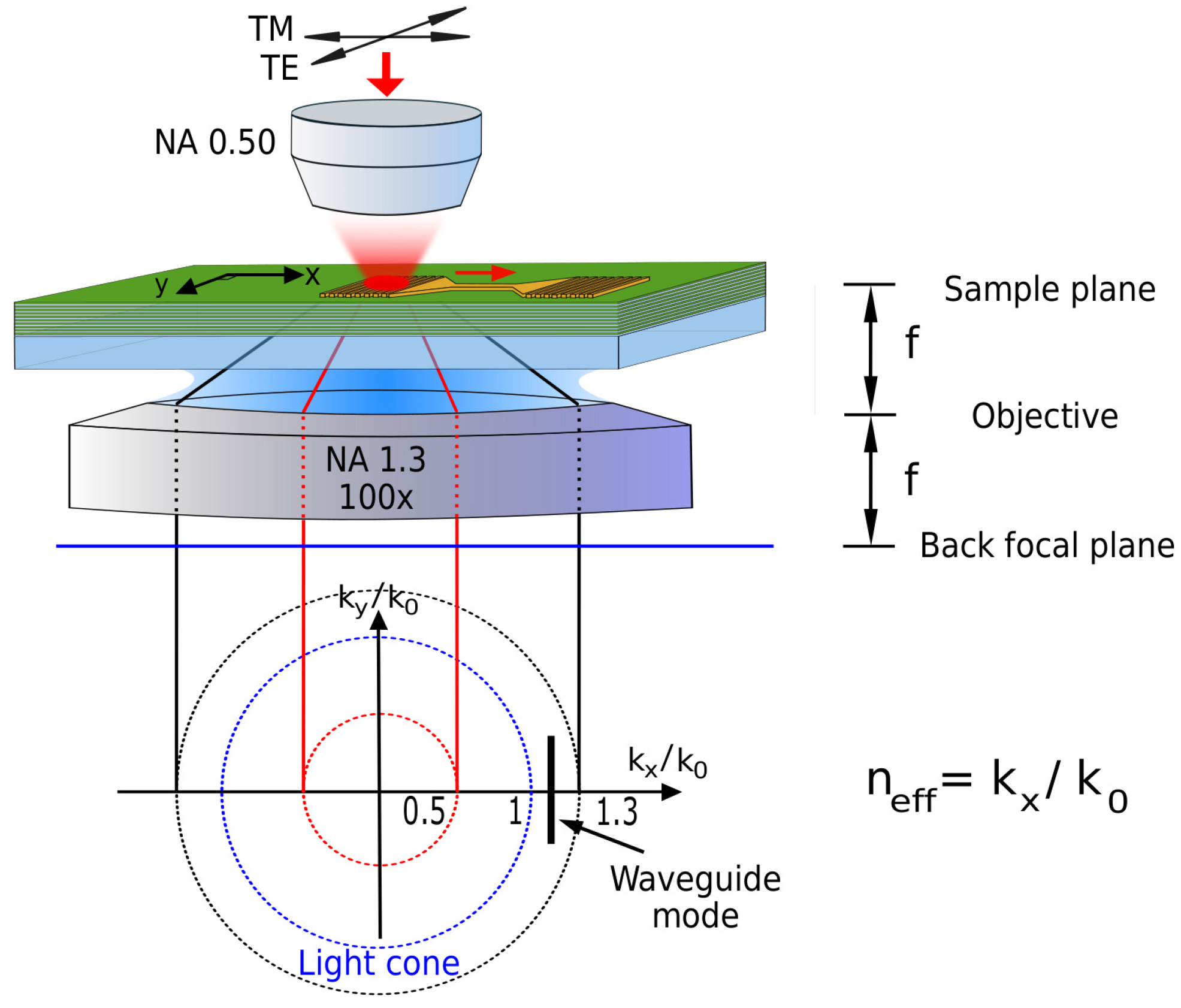
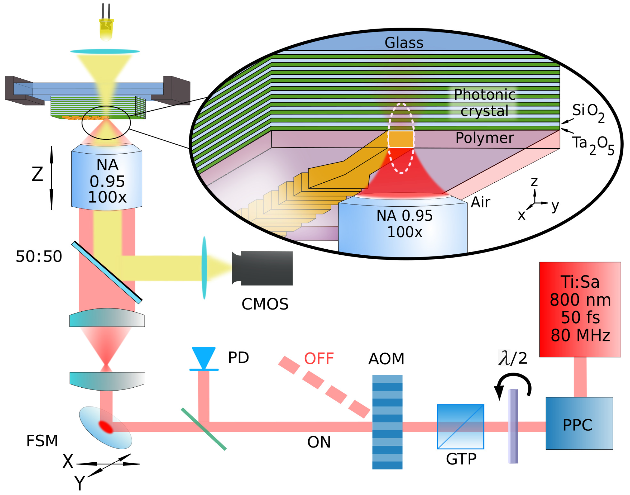
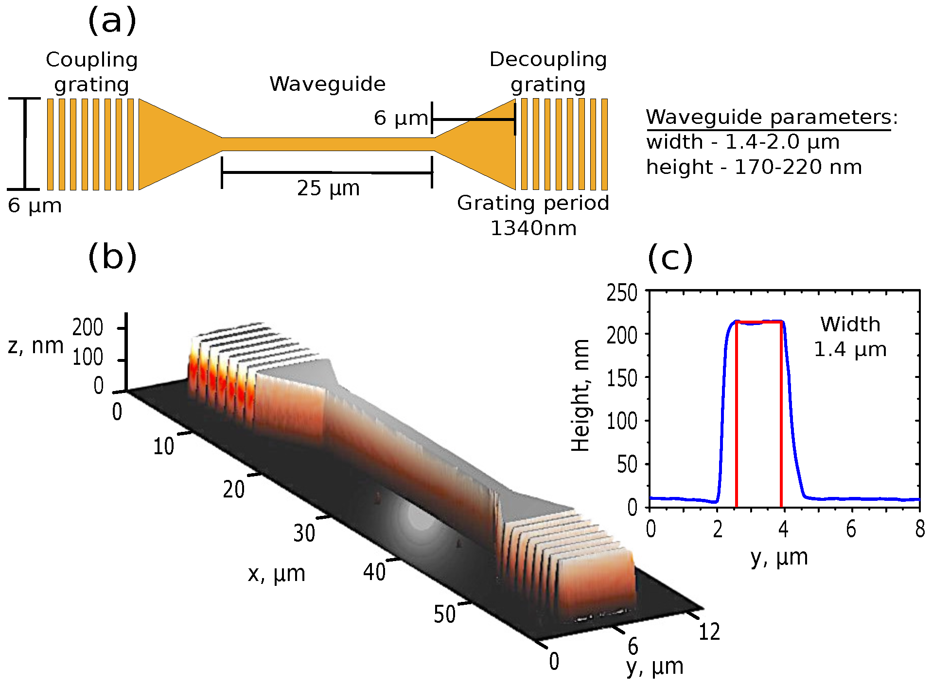
2. Materials and Methods
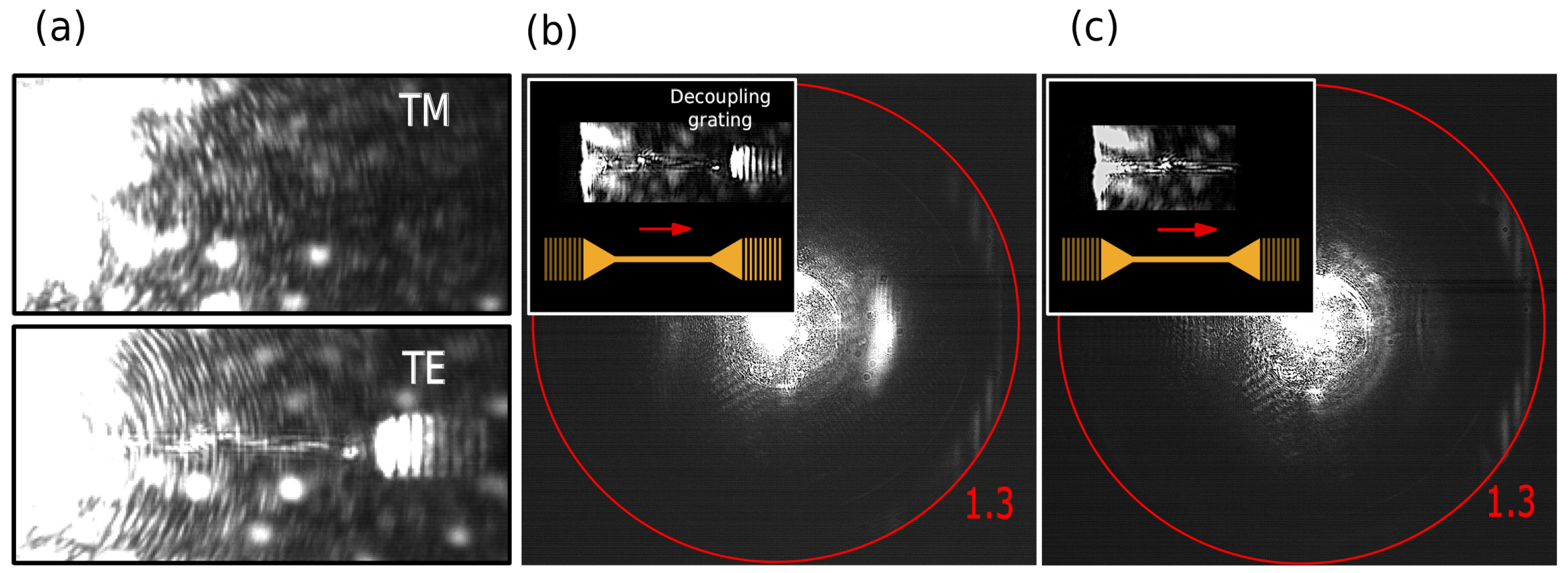
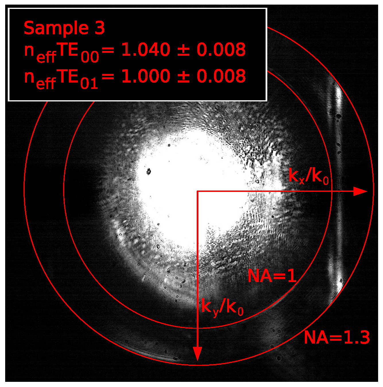
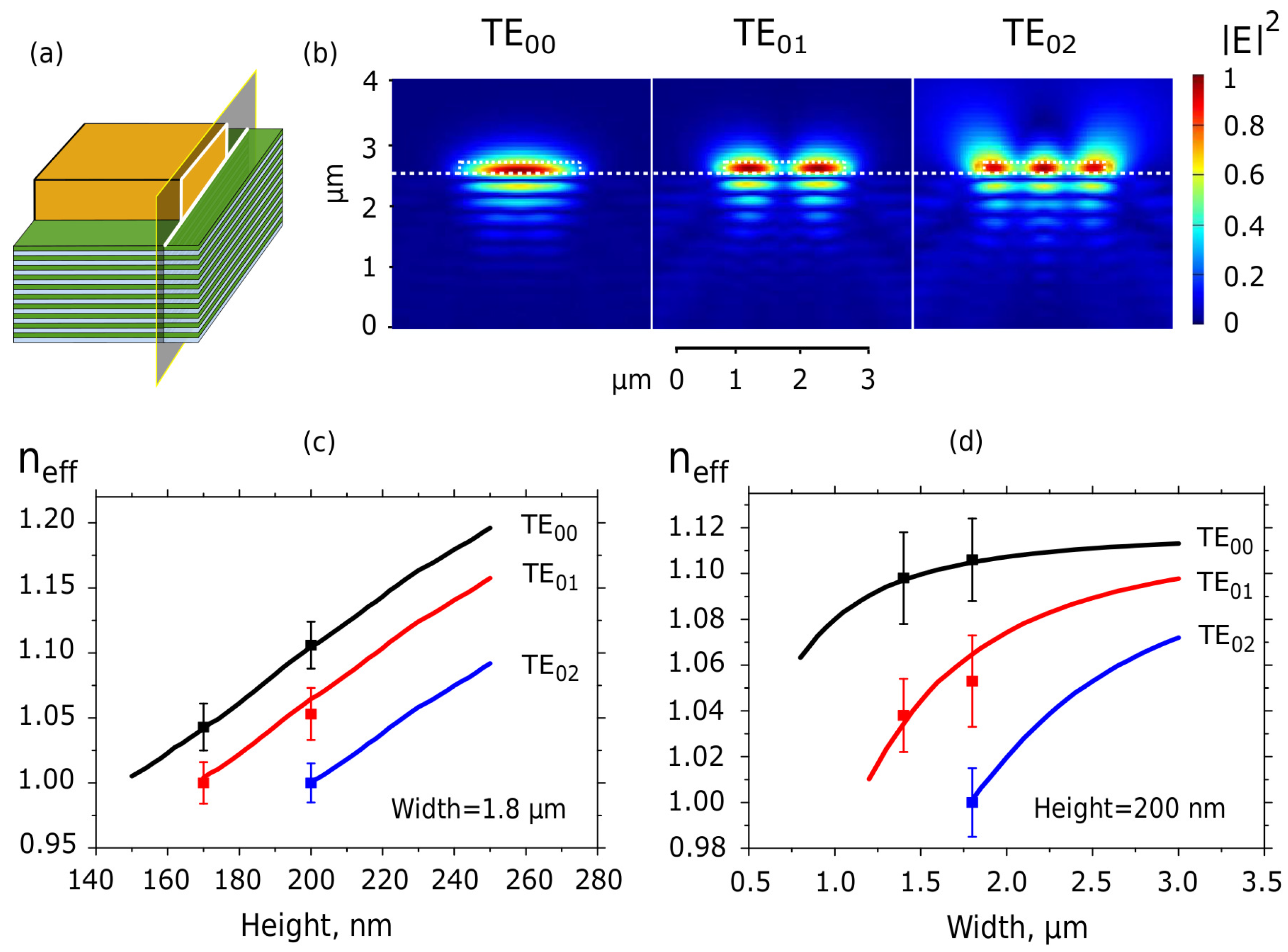
We used a custom 2PP setup for polymer film nanostructuring (Figure 1). Radiation from the source (Ti:Sa femtosecond laser, 800 nm, 80 MHz repetition rate, 50 fs pulse duration) passed through a pulse precompressor (PPC) to compensate for positive dispersion introduced by optical elements. A system of a halfwave plate λ /2 in a rotational motorized stage, a Glan–Taylor prism (GTP) and a photodiode (PD) controlled the average power of incident radiation with the accuracy of 0.1 mW. Acoustooptical modulator (AOM) served as a fast shutter. The fast steering mirror (FSM) provided the beam waist movement within the sample plane ( X Y ) with the accuracy of 1 nm in the field of 60 μ m × 60 μ m and a piezoelectric stage moved the laser beam waist in a perpendicular direction (Z) with the accuracy of 5 nm in the travel range of 200 μ m. The laser beam was tightly focused by an air objective (100×, numerical aperture (NA) = 0.95). The sample was mounted in an upside-down position on a motorized microscopic table because the photonic crystal is not transparent for incident radiation. The experimental setup was completely automatic. The polymerisation process was visualized and controlled by a CMOS camera DCC1545M (Thorlabs Inc, Newton, New Jersey, USA).
The photonic device height was controlled by the thickness of a polymer film. Polymer photoresist SU-8 2015 had been preliminarily diluted with a corresponding developer mr-Dev 600 to achieve necessary thickness by a standard spin-coating procedure (10 s 500 rpm, 30 s 2000 rpm). The polymer film was nanostructured in an overexposure regime, providing that the size of polymerisable volume (voxel) was much larger than polymer film thickness. This guaranteed the perfect rectangular cross-section of the BSW waveguides. The optimal exposition parameters were determined to be 11 mW of incident power, and 5 μ m/s of beam waist speed. The waveguide width was controlled by the number of scans with 100 nm accuracy.
As a platform for BSW-supporting photonic devices, we have chosen a 1D photonic crystal consisting of 10 pairs of alternating layers of SiO 2 (thickness = 140 nm, n S i O 2 = 1 . 53 at λ = 670 nm) and Ta 2 O 5 (thickness = 98 nm, n T a 2 O 5 = 2 . 086 at λ = 670 nm) sputtered on a cover glass with the thickness of 170 μ m. To eliminate the excitation of BSW on the surface of bare photonic crystal, the topmost layer was T a 2 O 5 . According to numerical calculations, the height of BSW waveguides and thickness of the polymer film should be in the range of 140–280 nm to efficiently excite the BSW.
Propagation of radiation in manufactured photonic devices was studied by leakage radiation microscopy (LRM). This simple technique allows for simultaneously visualizing the direct and Fourier plane, and analyse the efficiency of coupling as well as mode structure (Figure 2) [36]. A collimated beam from a diode laser source with 670 nm wavelength was focused by an air objective (NA = 0.5). The polarisation of incident and transmitted radiation were controlled by two Glan–Taylor prisms. The leakage radiation was collected by an oil immersion objective (NA = 1.3). The back focal plane (BFP) and sample plane were simultaneously projected on two CMOS cameras. The intermediate back focal plane image and direct plane image were additionally constructed to perform accurate elimination of intense transmitted radiation and parasitic reflections. The typical recorded intensity map of a BFP image is presented in Figure 2. It is expected to be a set of three concentric circles and a number of vertical stripes. The smallest circle corresponds to the transmitted radiation and its maximal radius is defined by the numerical aperture of the focusing objective (NA = 0.5). The largest one is defined by the numerical aperture of the oil-immersion objective that collects leakage radiation (NA = 1.3). The intermediate circle indicates the light cone in air and has the radius corresponding to NA = 1. The BSW waveguide modes should appear as vertical stripes between the circles with NA = 1 and NA = 1.3 [37]. The position of the intersecting point of the X-axis and every stripe defines the effective refractive indices of distinctive modes: n e f f = k x / k 0 .

3. Results

A schematic view of a BSW-supporting photonic device is presented in Figure 3a. It consisted of coupling and decoupling diffraction gratings, focusing and defocusing triangles, and a waveguide part. A diffraction grating coupling scheme provides efficient and compact excitation of BSW. The period of gratings (1340 nm) fulfilled wavevector-matching condition to guide incident radiation into the second diffraction order. Focusing and defocusing triangles enhance the efficiency of coupling [38]. The waveguide part is the main element of the device. Its geometry defines the mode structure of propagating radiation. We fixed the lateral size and the period of gratings, the size of triangles and waveguide length, while the height of the waveguide was varied in the range of 170–220 nm and the width of the waveguide was varied in the range of 1400–2000 nm. We fabricated four samples: sample 1 (height = 200 ± 10 nm, width = 1800 ± 100 nm), sample 2 (height = 200 ± 10 nm, width = 1400 ± 100 nm), sample 3 (height = 170 ± 10 nm, width = 1800 ± 100 nm), and sample 4 (height = 215 ± 10 nm, width = 2000 ± 100 nm). The quality and geometrical parameters of nanostructures were measured by atomic force microscopy (AFM) in contact mode regime. The AFM image of sample 2 is presented in Figure 3b. Non-square form of the cross-section (Figure 3c) may be attributed to the finite size of AFM probe.
Figure 4a shows a direct plane image of the device under illumination of the coupling (left) grating by focused radiation with transverse electric (TE)-polarisation (perpendicular to the waveguide) or transverse magnetic (TM)-polarisation (parallel to the waveguide). There is no mode propagation for TM-polarised light, only a bright spot of incident radiation scattered from the coupling diffraction grating may be observed (Figure 4a, top). Change in the polarisation results in the appearance of a bright grating-shaped reflex at the right end of the waveguide (Figure 4a, bottom) attributed to radiation emitted from decoupling grating. This experimentally observed polarisation sensitivity is consistent with the results found in literature for photonic crystals with similar geometry [19] as well as preliminary calculations made by transfer matrix approach.
To perform more accurate analysis, an image of the BFP was recorded. To make BFP images more clear, the intense radiation transmitted through the coupling grating was eliminated by a vertical block mounted in the intermediate direct plane image. Figure 4b,c shows two BFP images of sample 4 illuminated by TE-polarised incident light. Corresponding direct plane images and schematic views of the device are presented in the inset for comparison. One can see a central bright circle corresponding to the transmitted scattered radiation, an oval-shape reflex at the right side of the circle (Figure 4b), and a set of weak vertical stripes that is related to different BSW modes propagating in the waveguide of the device. Closing the decoupling diffraction grating in the intermediate direct plane image results in disappearance of the oval-shape reflex in the BFP image (Figure 4c). Thus, it can be attributed to the first diffraction order of the decoupling grating.
Using the BFP images, the effective refractive indices of BSW waveguide modes can be determined. Figure 5 depicts the BFP image of sample 3 and the circles defined the numerical aperture of the collecting objective and the light cone. The waveguide of the sample 3 supports only two BSW-modes. From the known NA = 1.3 of the objective and the position of the intersecting point of the X-axis and every stripe, the effective refractive index for distinctive modes may be calculated as n e f f = k x / k 0 . Stripe width defines the experimental error. We attributed the mode with the largest effective refractive index to TE 00 mode, and the second mode to TE 01 mode. The obtained effective refractive index values are presented in Figure 5.
The same procedure was conducted for other three samples. Obtained values of the effective refractive index of every mode and geometrical parameters of the waveguides of the samples are shown in Table 1. With the increase of polymer waveguide height as well as width, the effective refractive indices of modes and the number of modes are increasing. This indicates that electromagnetic field confinement in the polymer waveguide is enhancing with the increase of waveguide size.

4. Discussion

To accurately determine the mode structure in proposed BSW devices, we performed numerical calculations by the finite-difference time domain (FDTD) method. Model structure Figure 6a consisted of glass substrate (n = 1.52) with the infinite thickness, photonic crystal, the geometry and material that reproduced the experimental sample, and a polymer waveguide (n = 1.58) whose height end width was varied. The calculations performed for the sample 1 show that the waveguide sustains three BSW modes whose cross-sectional intensity distribution is presented in Figure 6b. The intensity pattern of the first mode T E 00 has only one lobe and demonstrates the best confinement in the waveguide compared to other two modes. The results of calculation of modes effective refractive indices on waveguide height at fixed width and on waveguide width at fixed height are shown by solid lines on Figure 6c,d, respectively. The effective refractive indices values as well as number of modes grow with the increase of both the waveguide height and width. The experimental values of n e f f obtained for samples 1–3 are presented in the same figure by dots and demonstrate a good agreement with calculated ones.

5. Conclusions

In conclusion, we have demonstrated applicability of the femtosecond laser polymerisation technique to nanofabrication of BSW-supporting integrated photonics devices. A novel photonic device with a compact excitation scheme was fabricated with a nanometer control of geometrical parameters in a single exposure procedure. We have experimentally observed and studied the excitation and propagation of BSW waveguide modes in a visible range in fabricated devices. We also performed numerical calculations that are in good agreement with experimental results. This agreement is a strong confirmation of the perfect rectangular shape of the waveguide. The results prove that the femtosecond laser polymerisation technique is well suited for realization of planar BSW-based integrated optics devices in a large variety of complex designs.
References

Acknowledgments

This work was partially supported by the Russian Foundation for Basic Research (No. 17-02-01419, 2PP setup development, sample fabrication, FDTD calculations), the Russian Science Foundation (No. 15-12-00065, LRM measurements) and Ministry of Education and Science of the Russian Federation (contract 14.W03.31.0008, development of LRM setup).

Author Contributions

K.A.A. and V.O.B. assembled the 2PP setup; K.A.A., N.G.K., K.R.S., I.M.A. and V.O.B. fabricated the samples; D.N.G. and V.O.B. assembled the LRM setup and conducted the LRM experiments; K.R.S. performed the numerical simulations; I.M.A. performed the AFM measurements; K.A.A. prepared the initial draft of the manuscript, D.N.G. prepared the figures; All the co-authors contributed to the discussion of the results and preparation of the manuscript.

Conflicts of Interest

The authors declare no conflict of interest.

References

  1. Maradudin, A.A.; Sambles, J.R.; Barnes, W.L. Modern Plasmonics; Elsevier: Amsterdam, The Netherlands, 2014. [Google Scholar]
  2. Yeh, P.; Yariv, A.; Hong, C.S. Electromagnetic propagation in periodic stratified media. I. General theory. J. Opt. Soc. Am. 1977, 67, 423–438. [Google Scholar] [CrossRef]
  3. Ramos-Mendieta, F.; Halevi, P. Electromagnetic surface modes of a dielectric superlattice: The supercell method. J. Opt. Soc. Am. B 1997, 14, 370–381. [Google Scholar] [CrossRef]
  4. Dubey, R.; Barakat, E.; Häyrinen, M.; Roussey, M.; Honkanen, S.K.; Kuittinen, M.; Herzig, H.P. Experimental investigation of the propagation properties of bloch surface waves on dielectric multilayer platform. J. Eur. Opt. Soc. Rapid Publ. 2017, 13, 5. [Google Scholar] [CrossRef]
  5. Badugu, R.; Mao, J.; Blair, S.; Zhang, D.; Descrovi, E.; Angelini, A.; Huo, Y.; Lakowicz, J.R. Bloch Surface Wave-Coupled Emission at Ultraviolet Wavelengths. J. Phys. Chem. C 2016, 120, 28727–28734. [Google Scholar] [CrossRef] [PubMed]
  6. Li, Y.; Yang, T.; Song, S.; Pang, Z.; Du, G.; Han, S. Phase properties of Bloch surface waves and their sensing applications. Appl. Phys. Lett. 2013, 103, 041116. [Google Scholar] [CrossRef]
  7. Paeder, V.; Musi, V.; Hvozdara, L.; Herminjard, S.; Herzig, H. Detection of protein aggregation with a Bloch surface wave based sensor. Sens. Actuators B Chem. 2011, 157, 260–264. [Google Scholar] [CrossRef]
  8. Qiao, H.; Soeriyadi, A.H.; Guan, B.; Reece, P.J.; Gooding, J.J. The analytical performance of a porous silicon Bloch surface wave biosensors as protease biosensor. Sens. Actuators B Chem. 2015, 211, 469–475. [Google Scholar] [CrossRef]
  9. Giorgis, F.; Descrovi, E.; Summonte, C.; Dominici, L.; Michelotti, F. Experimental determination of the sensitivity of Bloch surface waves based sensors. Opt. Express 2010, 18, 8087–8093. [Google Scholar] [CrossRef] [PubMed]
  10. Rivolo, P.; Michelotti, F.; Frascella, F.; Digregorio, G.; Mandracci, P.; Dominici, L.; Giorgis, F.; Descrovi, E. Real time secondary antibody detection by means of silicon-based multilayers sustaining Bloch surface waves. Sens. Actuators B Chem. 2012, 161, 1046–1052. [Google Scholar] [CrossRef]
  11. Frascella, F.; Ricciardi, S.; Rivolo, P.; Moi, V.; Giorgis, F.; Descrovi, E.; Michelotti, F.; Munzert, P.; Danz, N.; Napione, L.; et al. A fluorescent one-dimensional photonic crystal for label-free biosensing based on Bloch surface waves. Sensors 2013, 13, 2011–2022. [Google Scholar] [CrossRef] [PubMed]
  12. Sinibaldi, A.; Rizzo, R.; Figliozzi, G.; Descrovi, E.; Danz, N.; Munzert, P.; Anopchenko, A.; Michelotti, F. A full ellipsometric approach to optical sensing with Bloch surface waves on photonic crystals. Opt. Express 2013, 21, 23331–23344. [Google Scholar] [CrossRef] [PubMed]
  13. Delfan, A.; Liscidini, M.; Sipe, J.E. Surface enhanced Raman scattering in the presence of multilayer dielectric structures. J. Opt. Soc. Am. B 2012, 29, 1863–1874. [Google Scholar] [CrossRef]
  14. Soboleva, I.; Descrovi, E.; Summonte, C.; Fedyanin, A.; Giorgis, F. Fluorescence emission enhanced by surface electromagnetic waves on one-dimensional photonic crystals. Appl. Phys. Lett. 2009, 94, 231122. [Google Scholar] [CrossRef]
  15. Romodina, M.; Soboleva, I.; Musorin, A.; Nakamura, Y.; Inoue, M.; Fedyanin, A.A. Bloch-surface-wave- induced Fano resonance in magnetophotonic crystals. Phys. Rev. B 2017, 96, 081401. [Google Scholar] [CrossRef]
  16. Soboleva, I.; Moskalenko, V.; Fedyanin, A. Giant Goos-Hänchen effect and Fano resonance at photonic crystal surfaces. Phys. Rev. Lett. 2012, 108, 123901. [Google Scholar] [CrossRef] [PubMed]
  17. Shilkin, D.A.; Lyubin, E.V.; Soboleva, I.V.; Fedyanin, A.A. Near-field probing of Bloch surface waves in a dielectric multilayer using photonic force microscopy. J. Opt. Soc. Am. B 2016, 33, 1120–1127. [Google Scholar] [CrossRef]
  18. Shilkin, D.A.; Lyubin, E.V.; Soboleva, I.V.; Fedyanin, A.A. Direct measurements of forces induced by Bloch surface waves in a one-dimensional photonic crystal. Opt. Lett. 2015, 40, 4883–4886. [Google Scholar] [CrossRef] [PubMed]
  19. Descrovi, E.; Sfez, T.; Quaglio, M.; Brunazzo, D.; Dominici, L.; Michelotti, F.; Herzig, H.P.; Martin, O.J.; Giorgis, F. Guided Bloch surface waves on ultrathin polymeric ridges. Nano Lett. 2010, 10, 2087–2091. [Google Scholar] [CrossRef] [PubMed]
  20. Angelini, A.; Lamberti, A.; Ricciardi, S.; Frascella, F.; Munzert, P.; De Leo, N.; Descrovi, E. In-plane 2D focusing of surface waves by ultrathin refractive structures. Opt. Lett. 2014, 39, 6391–6394. [Google Scholar] [CrossRef] [PubMed]
  21. Yu, L.; Barakat, E.; Di Francesco, J.; Herzig, H.P. Two-dimensional polymer grating and prism on Bloch surface waves platform. Opt. Express 2015, 23, 31640–31647. [Google Scholar] [CrossRef] [PubMed]
  22. Descrovi, E.; Barakat, E.; Angelini, A.; Munzert, P.; De Leo, N.; Boarino, L.; Giorgis, F.; Herzig, H.P. Leakage radiation interference microscopy. Opt. Lett. 2013, 38, 3374–3376. [Google Scholar] [CrossRef] [PubMed]
  23. Angelini, A.; Barakat, E.; Munzert, P.; Boarino, L.; De Leo, N.; Enrico, E.; Giorgis, F.; Herzig, H.P.; Pirri, C.F.; Descrovi, E. Focusing and extraction of light mediated by Bloch surface waves. Sci. Rep. 2014, 4, 5428. [Google Scholar] [CrossRef] [PubMed]
  24. Kim, M.S.; Vosoughi Lahijani, B.; Descharmes, N.; Straubel, J.; Negredo, F.; Rockstuhl, C.; Hayrinen, M.; Kuittinen, M.; Roussey, M.; et al. Subwavelength focusing of Bloch surface wave. ACS Photonics 2017, 4, 1477–1483. [Google Scholar] [CrossRef]
  25. Kovalevich, T.; Boyer, P.; Suarez, M.; Salut, R.; Kim, M.S.; Herzig, H.P.; Bernal, M.P.; Grosjean, T. Polarization controlled directional propagation of Bloch surface wave. Opt. Express 2017, 25, 5710–5715. [Google Scholar] [CrossRef] [PubMed]
  26. Dubey, R.; Lahijani, B.V.; Barakat, E.; Häyrinen, M.; Roussey, M.; Kuittinen, M.; Herzig, H.P. Near-field characterization of a Bloch-surface-wave-based 2D disk resonator. Opt. Lett. 2016, 41, 4867–4870. [Google Scholar] [CrossRef] [PubMed]
  27. Wang, R.; Xia, H.; Zhang, D.; Chen, J.; Zhu, L.; Wang, Y.; Yang, E.; Zang, T.; Wen, X.; Zou, G.; et al. Bloch surface waves confined in one dimension with a single polymeric nanofibre. Nat. Commun. 2017, 8, 14330. [Google Scholar] [CrossRef] [PubMed]
  28. Sfez, T.; Descrovi, E.; Yu, L.; Brunazzo, D.; Quaglio, M.; Dominici, L.; Nakagawa, W.; Michelotti, F.; Giorgis, F.; Martin, O.J.; et al. Bloch surface waves in ultrathin waveguides: Near-field investigation of mode polarization and propagation. J. Opt. Soc. Am. B 2010, 27, 1617–1625. [Google Scholar] [CrossRef]
  29. Wu, X.; Barakat, E.; Yu, L.; Sun, L.; Wang, J.; Tan, Q.; Herzig, H. Phase-sensitive near field Investigation of Bloch surface wave propagation in curved waveguides. J. Eur. Opt. Soc. Rapid Publ. 2014, 9, 14049. [Google Scholar] [CrossRef]
  30. Yu, L.; Barakat, E.; Nakagawa, W.; Herzig, H.P. Investigation of ultra-thin waveguide arrays on a Bloch surface wave platform. J. Opt. Soc. Am. B 2014, 31, 2996–3000. [Google Scholar] [CrossRef]
  31. Wollhofen, R.; Katzmann, J.; Hrelescu, C.; Jacak, J.; Klar, T.A. 120 nm resolution and 55 nm structure size in STED-lithography. Opt. Express 2013, 21, 10831–10840. [Google Scholar] [CrossRef] [PubMed]
  32. Paz, V.F.; Emons, M.; Obata, K.; Ovsianikov, A.; Peterhänsel, S.; Frenner, K.; Reinhardt, C.; Chichkov, B.; Morgner, U.; Osten, W. Development of functional sub-100 nm structures with 3D two-photon polymerization technique and optical methods for characterization. J. Laser Appl. 2012, 24, 042004. [Google Scholar] [CrossRef]
  33. Petrov, A.K.; Bessonov, V.O.; Abrashitova, K.A.; Kokareva, N.G.; Safronov, K.R.; Barannikov, A.A.; Ershov, P.A.; Klimova, N.B.; Lyatun, I.I.; Yunkin, V.A.; Polikarpov, M.; Snigireva, I.; Fedyanin, A.A.; Snigirev, A. Polymer X-ray refractive nano-lenses fabricated by additive technology. Opt. Express 2017, 25, 14173–14181. [Google Scholar] [CrossRef] [PubMed]
  34. Stampfl, J.; Liska, R.; Ovsianikov, A. Multiphoton Lithography: Techniques, Materials, and Applications; John Wiley & Sons: Hoboken, NJ, USA, 2016. [Google Scholar]
  35. Malinauskas, M.; Farsari, M.; Piskarskas, A.; Juodkazis, S. Ultrafast laser nanostructuring of photopolymers: A decade of advances. Phys. Rep. 2013, 533, 1–31. [Google Scholar] [CrossRef]
  36. Drezet, A.; Hohenau, A.; Stepanov, A.L.; Ditlbacher, H.; Steinberger, B.; Galler, N.; Aussenegg, F.R.; Leitner, A.; Krenn, J.R. How to erase surface plasmon fringes. Appl. Phys. Lett. 2006, 89, 091117. [Google Scholar] [CrossRef]
  37. Massenot, S.; Grandidier, J.; Bouhelier, A.; Colas des Francs, G.; Markey, L.; Weeber, J.C.; Dereux, A.; Renger, J.; Gonzàlez, M.; Quidant, R. Polymer-metal waveguides characterization by Fourier plane leakage radiation microscopy. Appl. Phys. Lett. 2007, 91, 243102. [Google Scholar] [CrossRef]
  38. Holmgaard, T.; Bozhevolnyi, S.I.; Markey, L.; Dereux, A. Dielectric-loaded surface plasmon-polariton waveguides at telecommunication wavelengths: Excitation and characterization. Appl. Phys. Lett. 2008, 92, 011124. [Google Scholar] [CrossRef]
Figure 1. Femtosecond laser polymerisation lithography experimental scheme. The enlarged area represents an experimental sample being structured: a 1D photonic crystal with a polymer layer on the top.
Applsci 08 00063 g001
Figure 2. The scheme of a leakage radiation microscopy experiment with a schematical intensity map of a back focal plane image. The Bloch surface wave (BSW) modes appear as sharp narrow vertical stripes.
Applsci 08 00063 g002
Figure 3. (a) Schematic view of the fabricated photonic device. The sizes of gratings, triangles and waveguide length were fixed. Waveguide height and width were varied; (b) Atomic forece microscopy (AFM) image of manufactured photonic device (sample 2). (c) Waveguide cross-section (sample 2).
Applsci 08 00063 g003
Figure 4. (a) Direct plane image of the fabricated device for transverse electric- (TE-) and transverse magnetic- (TM-) polarisations of incident light. A grating-shaped spot on the right corresponds to the radiation, which was coupled to waveguide modes and subsequently radiated into the far field by decoupling grating; (b,c) back focal plane (BFP) and direct plane images of sample 4 with open (b) and closed (c) decoupling grating. Red circle defines numerical aperture (NA) = 1.3 of collecting objective.
Applsci 08 00063 g004
Figure 5. BFP image of sample 3. Two marked red concentric circles define the light line in air (inner) and NA of the collecting objective (external).
Applsci 08 00063 g005
Figure 6. (a) A schematic view of a model waveguide with a marked cross-section; (b) Electric field distribution in a waveguide cross-section for different modes, sustained by a model waveguide, whose size corresponds to sample 1; (c) The dependence of effective refractive index on waveguide height for different modes. The width of the waveguide is 1400 nm. Experiment—dots, theory—solid lines; (d) The dependence of effective refractive index on waveguide width for different modes. The height of the waveguide is 200 nm. Experiment—dots, theory—solid lines.
Applsci 08 00063 g006
Table 1. Effective refractive index values obtained from experimental Back focal plane (BFP) images for different Bloch surface wave (BSW) modes propagating in the samples with different geometrical parameters of the waveguide.
NameHeight, nmWidth, nmn eff TE 00 n eff TE 01 n eff TE 02
sample 1200 ± 101800 ± 1001.106 ± 0.0181.053 ± 0.0201.000 ± 0.015
sample 2200 ± 101400 ± 1001.098 ± 0.0201.038 ± 0.016-
sample 3170 ± 101800 ± 1001.040 ± 0.0081.000 ± 0.008-
sample 4215 ± 102000 ± 1001.161 ± 0.0101.116 ± 0.0101.037 ± 0.012

