Silicon Photonics towards Disaggregation of Resources in Data Centers
by
 and
and
Miltiadis Moralis-Pegios
1, 
Nikolaos Terzenidis
1,
George Mourgias-Alexandris
1 and
Konstantinos Vyrsokinos
2,* 
1
Department of Informatics, Aristotle University of Thessaloniki, 54124 Thessaloniki, Greece
2
Department of Physics, Aristotle University of Thessaloniki, 54124 Thessaloniki, Greece
*
Author to whom correspondence should be addressed.
Appl. Sci. 2018, 8(1), 83; https://doi.org/10.3390/app8010083
Submission received: 21 November 2017
/
Revised: 3 January 2018
/
Accepted: 4 January 2018
/
Published: 10 January 2018
(This article belongs to the Special Issue Optical Interconnects)
Abstract
:In this paper, we demonstrate two subsystems based on Silicon Photonics, towards meeting the network requirements imposed by disaggregation of resources in Data Centers. The first one utilizes a 4 × 4 Silicon photonics switching matrix, employing Mach Zehnder Interferometers (MZIs) with Electro-Optical phase shifters, directly controlled by a high speed Field Programmable Gate Array (FPGA) board for the successful implementation of a Bloom-Filter (BF)-label forwarding scheme. The FPGA is responsible for extracting the BF-label from the incoming optical packets, carrying out the BF-based forwarding function, determining the appropriate switching state and generating the corresponding control signals towards conveying incoming packets to the desired output port of the matrix. The BF-label based packet forwarding scheme allows rapid reconfiguration of the optical switch, while at the same time reduces the memory requirements of the node’s lookup table. Successful operation for 10 Gb/s data packets is reported for a 1 × 4 routing layout. The second subsystem utilizes three integrated spiral waveguides, with record-high 2.6 ns/mm2, delay versus footprint efficiency, along with two Semiconductor Optical Amplifier Mach-Zehnder Interferometer (SOA-MZI) wavelength converters, to construct a variable optical buffer and a Time Slot Interchange module. Error-free on-chip variable delay buffering from 6.5 ns up to 17.2 ns and successful timeslot interchanging for 10 Gb/s optical packets are presented.
1. Introduction
The Data Center (DC) architecture is relying on the interconnection of thousands or even hundreds of thousands of blade servers in the same location for the provision of advanced cloud services. Blades are considered the fundamental building block, with each unit encompassing a processor, a RAM module and a Network Interface Card (NIC). During the past years, the traditional model where the Hard Disks (HD) are incorporated into the blades, has evolved along with the emergence of Network-Attached-Storage containers empowered by optical interconnects. This recipe, named as storage disaggregation, is followed for optimizing storage resource utilization across the entire DC, but it is now expanding towards disaggregating other blade components i.e., processors and RAM modules. In addition to storage, emerging disaggregated DC architectures consider computing and memory elements as distinct homogenous pools of resources that are synergized over the DC interconnection network. This trend is dictated from the significant heterogeneity in resource usage per machine and workload [1,2] that leads to considerable resource underutilization, severely impacting cost and energy-efficiency of traditional DCs. Resource disaggregation at rack-scale, or even at DC-scale, [3,4,5] is becoming one of the major driving forces in transforming the DC architecture towards significant cost and energy savings [6,7] due to the fine control of available resources.
However, this brings in additional pressure to the DC network, that is already congested across the entire hierarchy, with typical oversubscription values of 3:1 to the north-south routes [8]. At the same time, the addition of new end-hosts into the DC network, as a consequence of the compute-memory elements disaggregation, will enforce a significant increase in the respective number of network addresses. Considering that the size of look-up tables at the switches is massive, from the thousands of blades already connected to the DC network, it is difficult for the network infrastructure to keep up with the disaggregation trend. Finally, rapid look-up table reconfiguration becomes a necessity in disaggregated scenarios since end-hosts change location or new hosts are added, as it is typically the case in Virtual Machine migration and network maintenance or extension, respectively [9].
The problem of look-up table size can be tackled by simplified forwarding schemes relying on Bloom filter (BF) labels, that have been shown to offer successful intra-datacenter routing with reduced memory requirements and enhanced multicasting credentials even in large DC enterprises [9,10,11]. BFs comprise probabilistic data structures that encode a set of elements into a single string, so that BF-based forwarding encodes, either the set of end-host addresses serviced by the next hop [9] or the forwarding identifiers of a certain multicast delivery tree [11]. This simplifies the look-up process into a membership check procedure and allows for storing a complete set of end-host addresses into a single memory entry, facilitating also look-up table updates once network topology changes are taking place. BF-label forwarding in large DC organizations has been shown to offer a reduction of at least 65% in fast memory requirements and a performance boost of 10% compared to a standard Ethernet packet forwarding scheme [9].
However, despite the advantages offered by schemes such as the BF-labelling approach, a shift in the switching technology is needed in order to meet these new bandwidth requirements. Silicon photonics arise as a promising technological candidate with high port count photonic fabrics already presented in the literature offering low cost due to their CMOS compatible fabrication processes and fast response time in the μs or even in the ns regime [12,13,14,15,16]. Moreover, they have been recently demonstrated in multi-casting routing schemes [15], as well as in software-programmable setups, exploiting photonic hardware-software co-development efforts [15,17,18,19,20,21,22] in order to gradually enrich their portfolio towards supporting the increased dynamicity and reconfigurability required in DC environments.
Moreover, the employment of Si photonics in optical packet routers can provide enhanced system-level performance with the provision of low loss and compact optical delay lines, the main building block in feed-forward optical buffering and Time-Slot Interchange units (TSI) [23]. Feed-forward optical buffers allow for a relatively simple optical packet storage mechanism, but with certain buffering time limits. TSIs on the other side are a more advanced buffering scheme, since they allow programmable time-slot rearrangement of optical packets towards reducing or even completely avoiding output-port contention. Both the feed-forward buffering and TSI modules rely on the use of optical switching stages and variable optical delay lines where the level of delay-line variability defines the buffering time and time-slot re-arrangement boundaries, respectively. Considering that optical architectures proposed for DCs promote the employment of limited size buffering at the switches for minimal latency [24], it is apparent that such schemes have an opportunity for turning into practical elements of real applications, towards avoiding latency- and energy-intensive electronic SerDes circuitry.
So, overall the Silicon Photonics technology platform can host both broadband, high speed, large scale switching matrices and low loss delay lines, that when utilized by a suitable control plane, are able to meet the stringent requirements imposed by disaggregation of resources in DC networks. An FPGA device with high number of I/O ports and ultrafast processing capabilities is the ideal tool for handling efficiently and fast the digital processing workload required for label processing and control signal generation, that in turn drives the active elements of the photonic packet router.
In this paper we present two network subsystems, that exploit the aforementioned advantages of the Silicon Photonics platform, towards meeting the requirements of disaggregated DCs. The first one is a BF-label forwarding optically-enabled node using a programmable Si-pho switching matrix and 10 Gb/s incoming optical packets that carry their BF-encoded destination address, as in-packet labels [25]. The demonstration was performed using a Si-based 4 × 4 electro-optic carrier injection switching matrix directly controlled by an amplifier-less and Digital to Analog (DAC)-less FPGA board, which mimics the role of an actual control plane that processes the packets’ labels and generates the proper electrical signals. The optically-enabled BF-based forwarding scheme is presented in a 1 × 4 switching scenario with 10 Gb/s data packets, that are successfully routed to the desired output port, while the look-up table content is updated every four packets in order to reflect network topology changes. The second subsystem is a variable optical delay-line buffer and Time-slot Interchanger module utilizing a set of three on-chip um scale Si-based integrated delay lines with low propagation loss and two, differentially-biased, SOA-MZI based wavelength converters (WC) [26]. The chip-scale SOI delay bank offers variable optical delay that ranges from 6.5 ns to 17.2 ns with a record-high on-chip delay versus footprint efficiency of 2.6 ns/mm2, improved by almost one order of magnitude compared to the 0.38 ns/mm2 state of the art implementations, featuring at least 10 ns on-chip delay [27,28,29,30,31,32,33,34]. This integrated variable SOI-based delay bank along with two WCs are utilized for the demonstration of a variable optical buffering scheme at 10 Gb/s, while the largest on-chip delay line of 17.2 ns is shown to perform successfully also in a 10 Gb/s optical TSI demonstration that uses two additional delay lines formed by fibers and two WC modules. Error-free operation at 10 Gb/s was obtained for both the variable optical buffer and the Time slot Interchanger module, with less than 5 dB power penalty.
2. Bloom Filter Labelling for Packet Switching with Photonic Integrated Switches
2.1. Concept
Bloom-Filter is a hash-based method for representing a set of elements to support membership queries. They were invented by Bloom [35] and, among other network applications [36], have been proposed as an efficient way of labelling packets or destinations, simplifying header processing to a few basic logic operations and avoiding the use of complex look-up functions [9]. Their employment has been promoted so far in Information-Centric networking [37,38] and more recently also in DC network environments [9,11,36,39], where they revealed significant reduction in memory size and cost requirements [9].
The BF labels are created by allocating a vector v of m bits, initially set to 0, and then choosing k independent hash functions each with range (1,…,m). For each element (a), that we want to group the bits at positions h1(a)…hk(a) in v are set to 1. To query if an element b is a member of this BF we check the bits at positions h1(b)…hk(b). If any of them is 0 then b is certainly not a member of the group. Otherwise, we can conjecture that b belongs to this group, even though there is a possibility that this is a wrong assumption, called a “false positive”. For n numbers of elements, the probability of this false positive occurring show good congruence with the approximation of:
In this respect, choosing k and m according to network requirements can minimize the probability of a false positive [35].
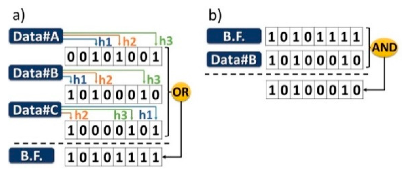
An example for better understanding the use of Bloom Filters is illustrated in Figure 1, where an 8-bit vector along with 3 hash functions h1, h2 and h3 are considered. Figure 1a depicts the construction process of a Bloom filter containing three different data elements in two stages. Initially, the representation for each element is generated using the hash functions and subsequently the three elements are encoded in a BF using a bitwise-OR operation. Figure 1b illustrates the inverse operation where a query for a single element (Data#B) is performed in the BF produced in Figure 1a. A bitwise-AND operation is performed between the Bloom filter and the element to be checked, with the result of this operation defining whether the element is a member of the Bloom Filter. In the case that the result is identical to the element’s representation then the element is possibly a member of the Bloom Filter, otherwise the element is definitely not a member.
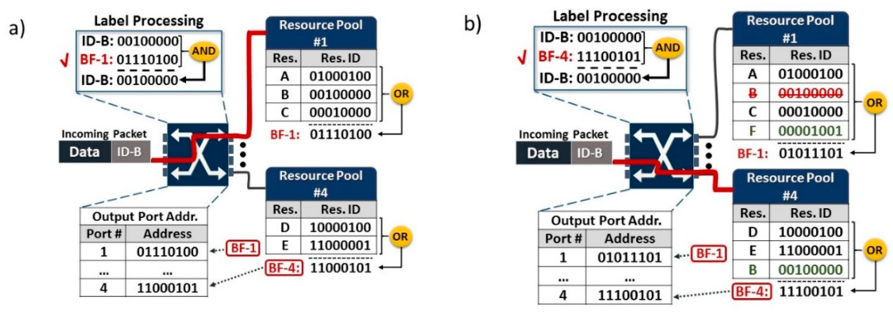
The proposed BF labelling concept for DCs is schematically illustrated in Figure 2 where each resource is associated with a designation address or ID following a traditional packet switching scheme. Figure 2a shows a switch with 4 output ports, where every port connects to a physical resource pool, which can encompass computing, memory and/or storage modules usually termed as bricks, in the DC environment. The length of the ID, and therefore the length of the resulting bloom filter, has to be chosen so that the possibility of false positives approaches effectively 0. The switch port connecting to the set of resources residing on the same physical resource pool (i.e., a tray or a rack incorporating several processor or memory or storage nodes) is addressed by a BF stemming from a bit-wise OR operation between the IDs of these resources. For example, BF-1 originating from the OR operation between the IDs of Res-A, Res-B and Res-C of the Resource Pool#1 becomes the address of switch port#1. Whenever an incoming packet destined for a certain Resource enters the switch, the packet header carrying the destination address ID is logically ANDed with the four BFs corresponding to the four switch outputs. In case the result of this AND operation is identical to the packet header, it means that the packet header is most probably a member of the BF and the packet is forwarded to the respective switch port. Figure 2a depicts the case where the incoming packet wants to access the Res-B segment. Its ID is being processed and is found to be a member of the BF corresponding to switch port#1. A subsequent network topology reconfiguration that will require the movement of Res-B from Resource pool#1 to Resource pool#4 as well as the entry of a new Resource (Res-F) into an empty segment of the Resource Pool#1 is presented in Figure 2b. Once the topology reconfiguration is completed, the new BFs corresponding to the switch ports are calculated and are fed to the switch as its new forwarding table information so that the incoming packets can continue to be directed to the desired resource. Figure 2b also depicts the example of a new packet entering the switch and destined again for Res-B. Its ID is now being processed and is found to be a member of the new BF corresponding to switch port#4. So, it becomes again successfully switched to Res-B that are now located at Resource Pool#4. This approach is in principle compatible with the virtual addresses assigned to memory pages in current computing schemes, where pages can be distributed among several memory modules.
2.2. Experimental Setup
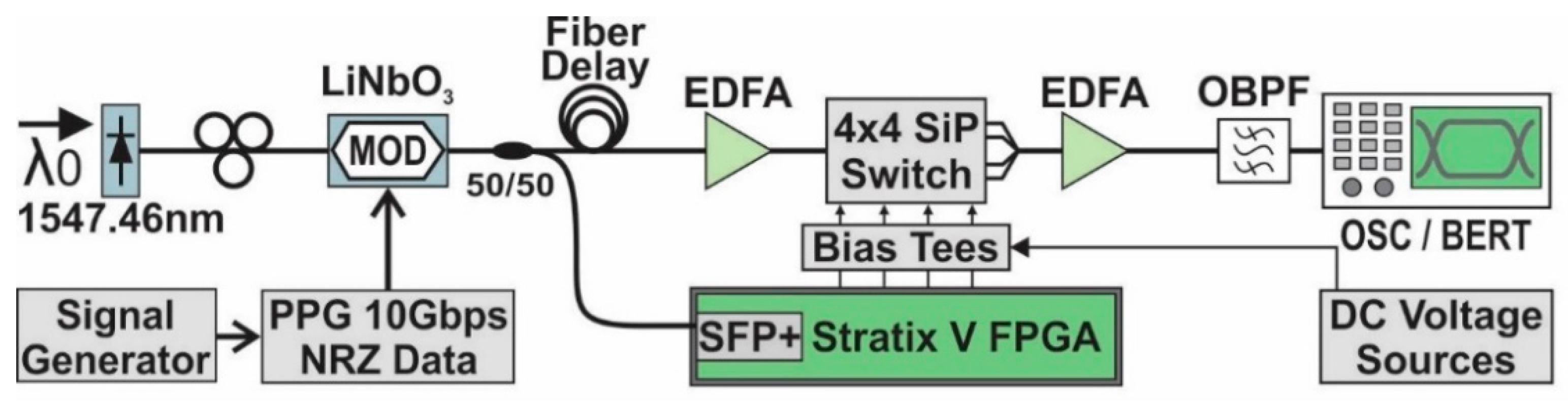
The concept described in detail in Section 2.1 was verified with the experimental setup illustrated in Figure 3.
A CW laser beam at 1547.76 nm was modulated via an Optilab 10 Gb/s LiNbO3 modulator driven by an Anritsu PPG so as to produce 200-bit long optical packets at 10 Gb/s. The packets were comprised by predefined 8-bit headers and 127 bit payload encoded with 27 − 1 NRZ data pattern. Successive packets were placed apart with a guard band of 6.5 ns in order to avoid imperfect switching during the switch ON/OFF times. An initialization sequence, equivalent to 2 consecutive K28.5 8 b/10 b codewords, is sent to provide word alignment for the FPGA. A 56-bit pattern of alternating 0 and 1 bits, equivalent to the Ethernet preamble, precedes the data packets to establish receiver clock synchronization at the beginning, while the continuous data transmission realized subsequently retains synchronization throughout the experiment. The guard-band duration of 6.5 ns (65 bits @ 10 Gb/s) were selected to be within the maximum running length of 66 bits that is supported by our SFP+ module in case 64/66 b encoding of 10 G Ethernet is used.
The packet stream was split by a 50/50 coupler into a fiber destined to the input port#3 of the 4 × 4 switch and a fiber destined to the FPGA. The optical stream destined to the FPGA was received by a commercial SFP+ module, where the information was converted to its electronic format prior performing the necessary deserialization, word-alignment and synchronization functions by the FPGA transceiver circuit. The 32-bit deserialized data stream was subsequently forwarded to the BF-label processing functions in order to generate the appropriate control signals for the switch. The required label bits were extracted from the data packet and compared with the BF-labels of the switch output ports according to the procedure described in Section 2.1. Every label bit is compared with the respective bit of the BF-labels assigned to the switch ports that are stored in a look-up table. In the event of a network topology reconfiguration, only this look-up table has to be updated with the new BF-labels. A separate look-up table contains the switch configuration settings for every input-output port combination. When a packet label matches the BF-label of a specific output port, the appropriate MZI control signals for successful forwarding are derived from this look-up table and are activated prior being serialized by the FPGA transceiver circuit and forwarded to the corresponding MZIs. The latency introduced by the FPGA following the data reception and until generating the switch control signals was measured to be approximately 452 ns, with 444 ns originating from the transceiver circuit and its constituent SerDes, word-alignment and synchronization functions and just 8 ns or 2 cycles originating from the BF-label processing operations. To counterbalance the FPGA BF-label forwarding latency, the optical packet stream was delayed in a fiber delay line prior entering the integrated switch. After exiting the switch, the optical packets were amplified and filtered in a 0.8 nm bandpass filter prior being recorded at a digital sampling oscilloscope and evaluated with a BER tester.
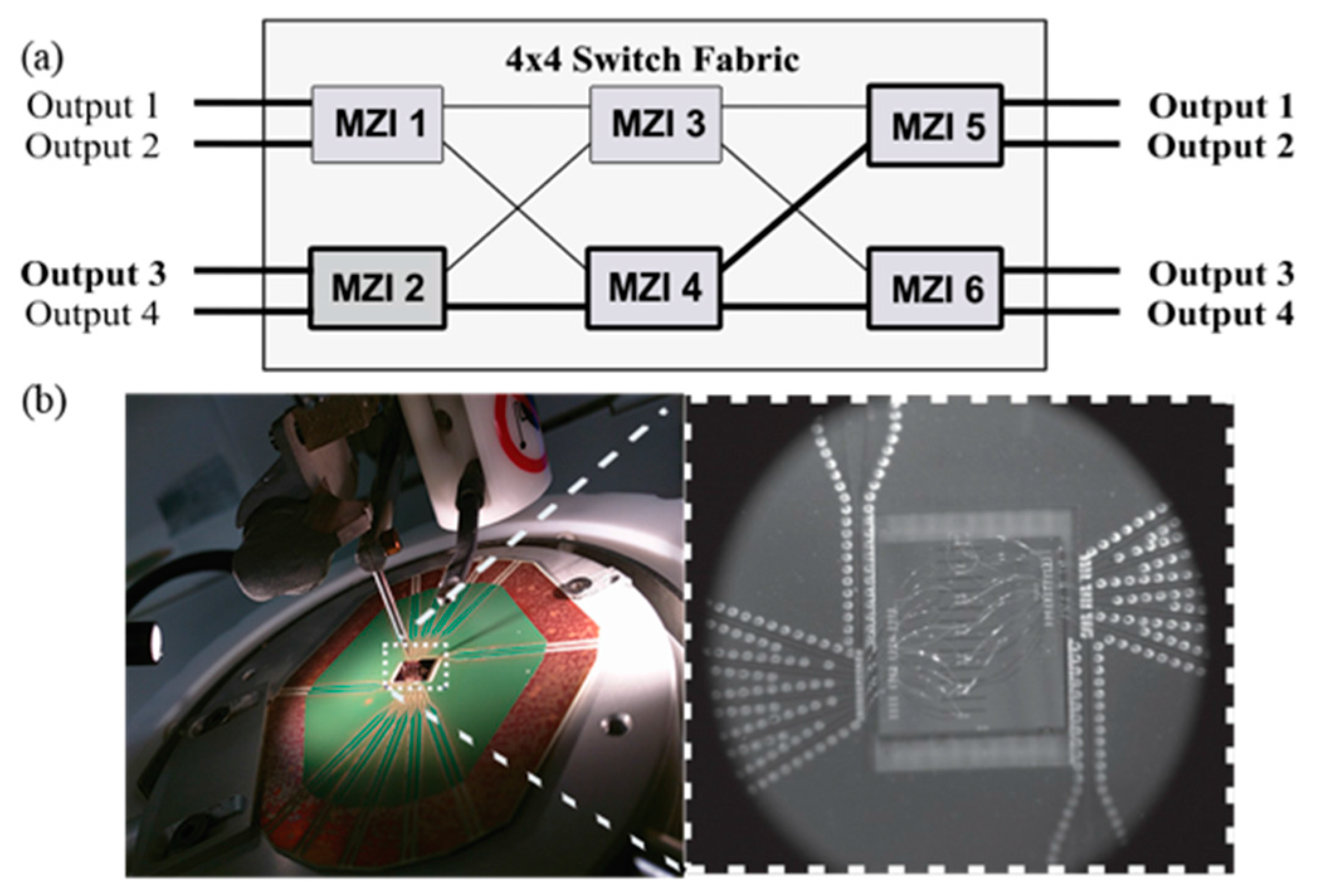
The 4 × 4 Si-pho switch used for the experimental demonstration is based on standard CMOS processes in 200 mm wafers with 220 nm × 400 nm Si waveguides on top of 2 μm SiO2. The slab height of the waveguides is 150 nm. The switch is composed from six MZI switches arranged in a Benes architecture, as illustrated in Figure 4a, providing non-blocking operation during packet forwarding. The chip is mounted on a high speed Printed Circuit Board (PCB) that fans out the pads from the phase shifters to SMA connectors placed at the edge of the PCB. Due to space limitations and the small pitch of the pads, the wire bonds from the phase shifters were in close proximity to the grating couplers, prohibiting in this way the use of a fiber-array for accessing simultaneously more than one input/output ports. Figure 4b depicts a photo of the packaged device, showing in more detail the very dense wiring connecting the MZIs to the PCB pads. Two electrical phase shifters (PS) are employed per interferometer, accounting for twelve in total.
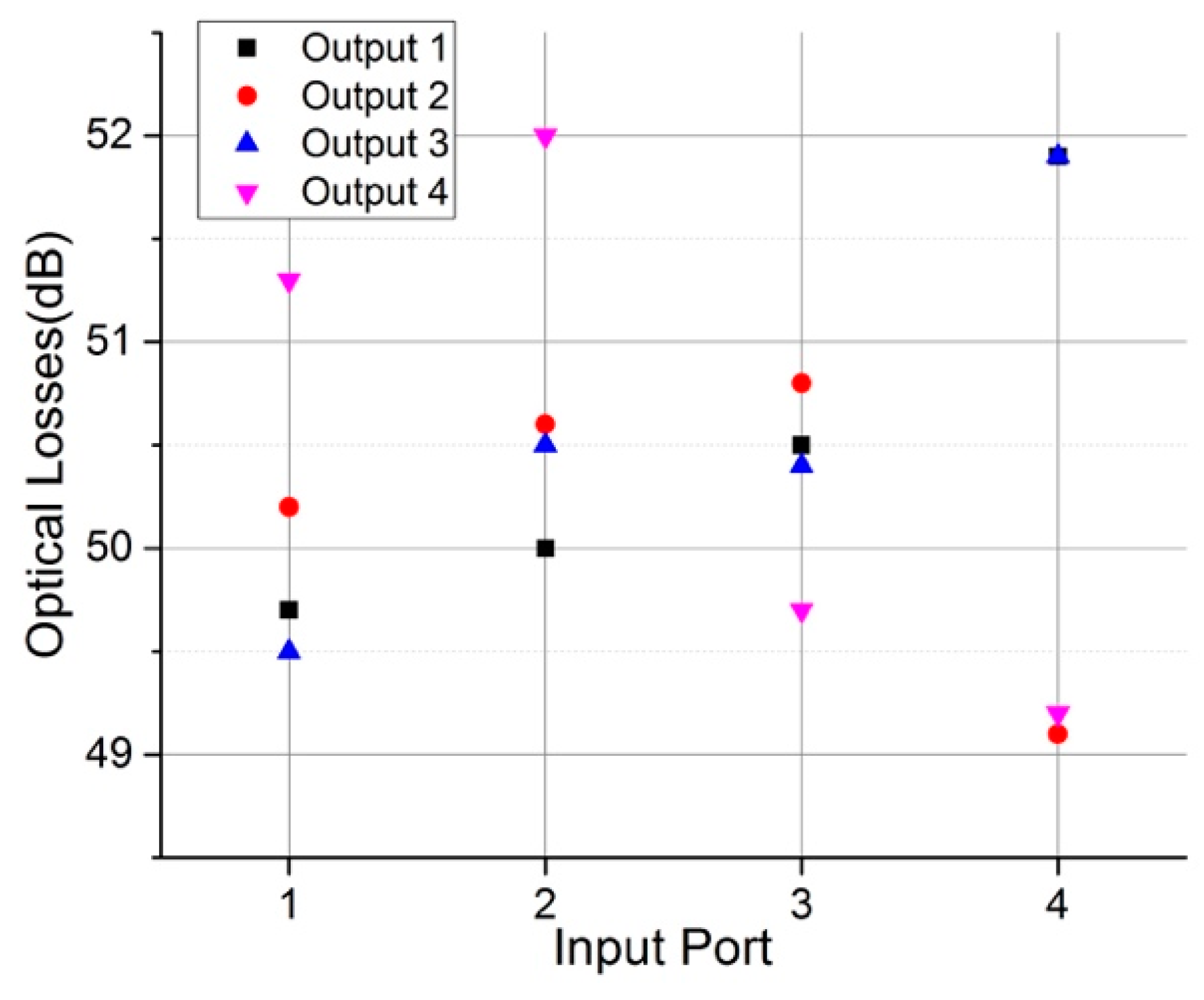
The electro-optical PSs of the MZIs are 1.25 mm long vertical PN diodes. Switching is realized by means of forward carrier injection so as to avoid the high Vpi requirements of the carrier depletion mechanism and to allow for the direct PS connection to the FPGA control ports without the intervention of amplifiers in the transmission line. Due to non-optimal fabrication process, the MZIs presented variation in the power required for setting in the BAR or CROSS state with the results presented in Table 1. The measurements reveal a Vπ value for the six MZIs in the range of 0.9–1.1 V. The power consumption in the two extreme cases of having all phase shifters turned on and turned off are 115 mW and 5.6 mW, respectively. Due to imperfect p-n junction fabrication that resulted to almost 9 dB insertion losses for every p-n junction, the optical losses for the entire matrix were found to be in the range of 48–52 dB depending on the input-output port pair as it is shown in Figure 5.
The cross-talk value of an individual MZI was measured to be in the range of 10 dB–18 dB. Moreover, the transfer function of the 4 × 4 switch has been measured by injecting light in port#3, while switching to all output ports was realized via biasing the phase shifters from a DC source. The results have already been reported in [40], with crosstalk ranging from 8 dB to 12 dB for 1535 nm–1550 nm operation.
The characterization of the switch in the time domain was performed by driving MZI#6 with RF signals, while the other MZIs were DC biased. The PN junctions were forward biased with two driving signals of 1 Vp-p coming from a Pulse Pattern Generator (PPG) for push pull operation of the MZI. The PPG was running at 200 MHz with 50% duty cycle pulses. Figure 6 illustrates the recorded optical trace revealing a rise and fall times of 0.8 ns and 1.2 ns, respectively. In the case of the single-drive MZI operation, the respective response times were higher with a rising time of 2.5 ns and a fall time of 3 ns.
For the Bloom Filter forwarding demonstration, the Si photonics switch chip was controlled by a Stratix V FPGA (Field Programmable Gate Array) board that provides up to 12.5 Gb/s control signals with a maximum peak voltage of with a 1.1 V. with a high and low level of 1.23 V and 0.15 V, respectively. The six MZIs were biased at the optimum operating point with an array of power supplies. The mixing of the RF and DC electrical signals was performed with six Bias-T devices that were connected to the SMA connectors leading to the upper phase shifter of each MZI. The electrical pulsed signal applied to the phase shifters had a peak power of ~0.9 V that was marginally adequate for obtaining a pi phase shift. The DC bias was set for all MZIs at the operating point where the highest possible extinction ratio between the two output ports was observed. In the demonstrated scenario MZI#4, #5 and #6 out of the six were controlled by respective FPGA outputs, while MZI#2 was DC biased to perform at its OFF state.
2.3. Results
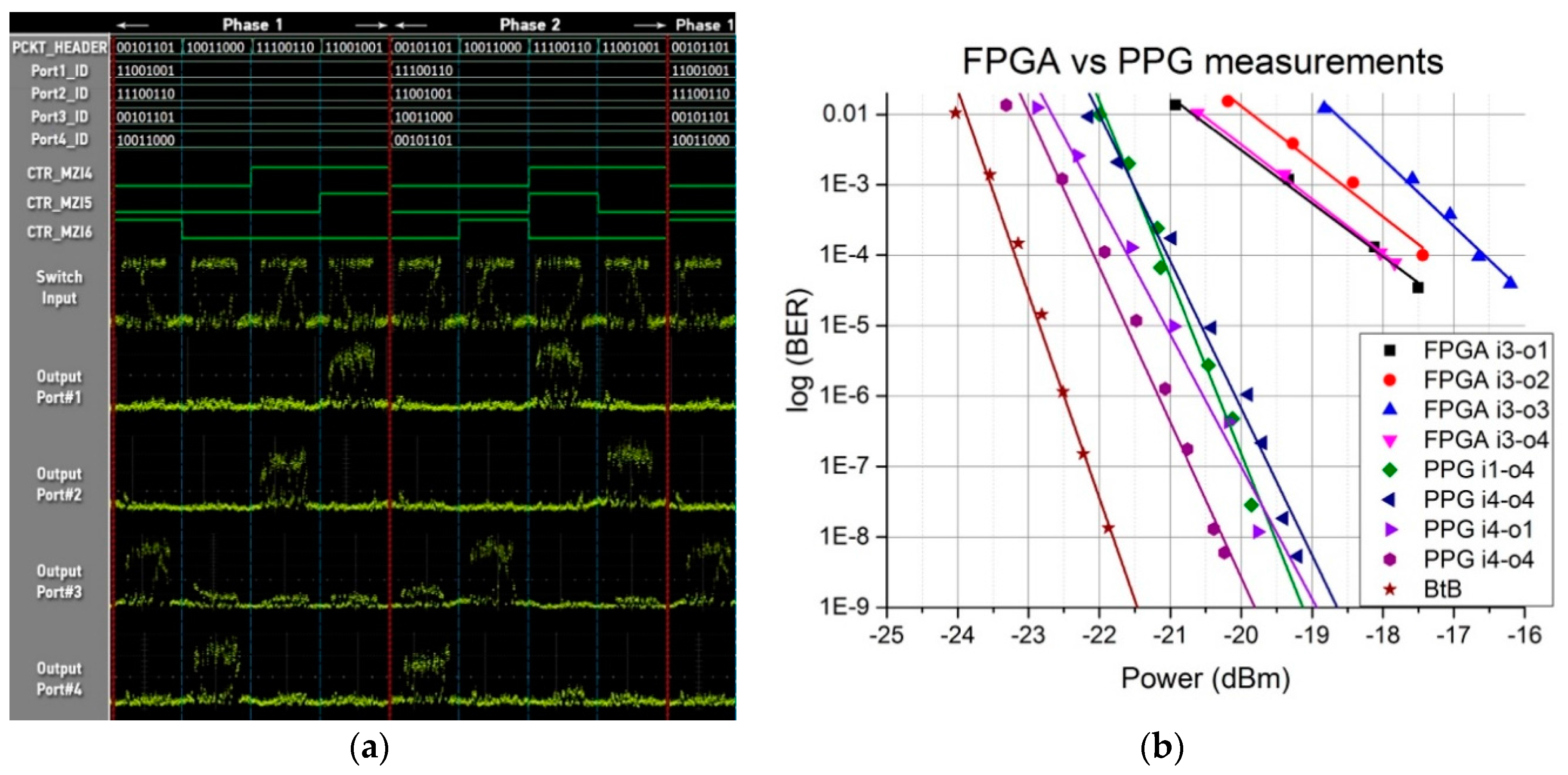
Figure 7a illustrates the oscilloscope traces obtained for two different phases (Phase#1 and #2), with every phase lasting for the duration of four data packets and corresponding to a different combination of BF-based addresses (IDs) for the four switch output ports. The first five rows in Figure 7 show the packet headers and the four output port IDs (Port1_ID, Port2_ID, Port3_ID, Port4_ID). Rows 6, 7 and 8 illustrate the respective control signals produced by the FPGA for driving MZIs 4–6 (CTR_MZI4, CTR_MZI5 CTR_MZI6) after processing the packet header information and the port ID.
During Phase#1, each of the four packets is routed to a different output port based on its header information and the respective Port ID. At the end of Phase#1, the four BFs corresponding to the respective port IDs get a new label, resembling the case of a change in the network topology and the new location of resources. This results into a different routing path for each packet even though every packet retains its header during both Phases. For example, the first packet with header ‘00101101’ is routed to Output port 3 during Phase 1 and to Output Port 4 during Phase 2. Figure 7a indicates proper routing functionality and switch re-configurability for all packets during both phases.
BER measurements were then performed, to evaluate the signal quality degradation, when optical packets are forwarded through the switch matrix utilizing the BF-labelling scheme. The 10 Gb/s packets were inserted in port 3 of the switching matrix and routed to all output ports. The BER measurements illustrated in Figure 7b revealed an error-floor at 10−4, which mainly stems from the limitations on the maximum current drawing enforced by the Pseudo Current Mode Logic (PCML) interface of the FPGA output transmitter channels. The PCML interface constrained the current to values lower than 10 mA, which translates to 9 mW of maximum electrical power applied to each MZI. This power ensures optimal switching only for MZI#5, according to Table 1, while all other switches required higher power levels for altering their state.
The PCML interface and the associated current drawing-based origin of the 10−4 error-rate was verified by replacing the FPGA board with a PPG capable to deliver programmable patterns up to 12.5 Gb/s with voltage levels up to 2.5 Vpp and without any limitations in current draining. Two (MZI#4, MZI#6) out of the three switches in the path i1/i4 to o1/o4 were controlled by the PPG, while MZI#2 was biased with a constant DC signal. The two electrical control signals had a voltage swing of 1 V and 1.1 V, respectively, and the BER performance is presented in Figure 7b. The enhanced ER of the switches from the unlimited current draining led to error-free operation up to 10−9, with a power penalty ranging between 1.2 dB–2.5 dB. This indicates that the use of DAC or amplification at the FPGA output can yield error-free operation at the expense of increased power consumption. The use of driving circuits to interface the FPGA with the MZIs yielding both optimal voltage and current driving levels has already been reported in [41] and can result in an extra power consumption of at least 1.2 W [42] for the whole 4 × 4 switch composed of 6 MZIs. As such, the capability to perform also in DAC- and amplifier-less mode allows for deciding upon the operational scheme based on the application-enforced signal quality and energy consumption requirements.
The ON/OFF suppression ratio between packets at the output of the switching matrix was measured to be 7 dB, mainly owing to the sub-optimal switching obtained at MZI#6. Given the fact that the 4 × 4 switching matrix is capable of providing cross-talk values up to 12 dB when driven by a DC electrical source and operating under optimal driving conditions [40], the utilization of a current amplification stage for optimally biasing the MZIs could in principle improve crosstalk up to 5 dB at the cost of extra power consumption. Improving cross-talk performance of the switch beyond this point, would involve modifications to the switch design. A number of different techniques have been already demonstrated towards this direction such as the use of a dilated Benes architecture [43] that could result in lower crosstalk, but would increase the number of stages, as well as the losses. Other approaches comprise the use of SOA’s in an MZI branch that could offer lossless operation along with lower crosstalk as in [44], or the modification of the 2 × 2 MZI basic building block to offer lower crosstalk as in [45].
3. Optical Buffering and TSI with Integrated Delay Lines
3.1. Concept
The disaggregated DC paradigm imposes stringent requirements on the interconnection network, creating new challenges in terms of bandwidth and forward latency on the DC switches. Specifically, failing to meet these latency requirements will result in underutilization of the disaggregated DC resources that cancels out the performance advantages disaggregation targets to. Considering that most of this latency is coming from o-e-o conversion, keeping the data in the optical domain is expected to significantly lower the end-to-end latency. However, contention resolution at the switching matrix, arises as a significant problem due to the lack of practical optical RAM, despite recent promising demonstrations [46]. A solution to mitigate this burden is limited-size optical buffering using optical delay lines, already proven advantageous in IP networks [47], in conjunction with the right protocol that can ensure reduced latency values in Disaggregated DC Interconnect (DCI) environments. In this direction feed-forward buffering schemes and TSIs might eventually have a new opportunity for turning into practical elements for real applications towards latency- and energy savings coming from power hungry electronic circuitry employed so far in DC routers.
Demonstrating such an optical based packet router in an integrated form mandates that the photonics platform should be capable both for switching the optical packets and also buffering them in suitable delay lines. This technology would then allow, the migration of fiber-based delaying and TSI deployments demonstrated so far [48,49,50] towards ultra-compact and highly-functional modules suitable for cooperation with integrated switch matrix designs, such as the one presented in Section 2.
The Thick-Silicon photonics platform holds the credentials for such an undertaking allowing the integration of long spiral waveguides, inducing delays of up to a few tens of nanoseconds, while maintaining a reasonable total power budget due to their extremely low-loss (<0.15 dB/cm). This buffering time can either be extended through the use of cascaded stages of feed-forward buffers, as demonstrated in [49], or it can be utilized more efficiently by a sophisticated optical switch architecture, as proposed in [51]. By employing this approach, throughput values higher than 80% can be achieved [51], even using ns inducing waveguides, showing the way for integrated functional sub-systems.
3.2. Experimental Setup and Results for Optical Packet Buffering
A close-up view of the SOI chip utilized is shown in Figure 8a. The chip is fabricated on a 4 μm SOI platform and comprises three spiral waveguides, all based on 4 μm thick, 1.875 μm wide strip waveguides separated by 2 μm gaps, while the Euler bends have a minimum bending radius of 36.9 μm allowing an effective bending radius of 69 μm for a 90° bend [51]. Despite the relatively narrow gap between adjacent waveguides in the spiral, optical radiative crosstalk in the fundamental mode is negligible, since the high confinement in the μm -scale waveguide core, renders very small any interaction with the sidewalls. A three-stage design was used to couple light to the strip waveguides ensuring single mode operation. Light was first butt-coupled from a single mode fiber to a 10 μm wide rib waveguide, that was subsequently tapered down to 3 μm width. A 350 μm long rib-to-strip converter was then employed to couple light into the strip waveguides [53]. Three waveguides were utilized with lengths of 0.52 m, 0.94 m and 1.46 m, which correspond to delay values of 6.5 ns, 11.3 ns and 17.2 ns at 1550 nm and are denoted as Delay 1, Delay 2 and Delay 3, respectively. The total insertion loss of the three delay lines was measured 20 dB, 25 dB and 30 dB respectively, while the input-output coupling loss was found to be 12.5 ± 0.5 dB and the propagation loss was estimated at 0.12 ± 0.01 dB/cm, in close agreement to the propagation loss values reported in [51]. Based on these measurements, the average delay versus loss efficiency is calculated at 0.93 dB/ns, while the delay versus footprint efficiency is found to be 2.6 ns/mm2 by dividing the 17.2 ns delay to the 4.4 × 1.5 mm2 footprint of the largest waveguide.
The experimental setup of the variable optical buffer is illustrated in Figure 8b. It comprises two cascaded WC stages (WC 1 and WC 2), fabricated by former CIPphotonics, interconnected with an intermediate delay stage. A 1550 nm laser beam is modulated in a Optilab LiNbO3 modulator, driven by an Anritsu Programmable Pattern Generator (PPG), to produce a periodic signal with a 256-bit period that incorporates three 35-bit-long 10 Gb/s NRZ data packets. Every packet consists of a 31-bit payload and a 4-bit header, while a 12-bit long inter-packet guardband is used between packets (I), (II) and packets (II), (III). The packet stream is split into two identical signals that are injected as push-pull control signals into the D and E ports of WC1. Three laser beams (λ1 = 1556.55 nm, λ2 = 1558.13 nm, λ3 = 1559.75 nm) are fed in separate LiNbO3 modulators driven by respective PPGs to realize 54-bit-long envelope signals at a 40 MHz frequency, which are multiplexed in an Arrayed Waveguide Grating (AWG) after being properly synchronized and are launched into port G of WC 1 as the WC 1 input signal. The WC 1 output signal is injected into the delay stage, which comprises an Opneti AWG demultiplexer, the integrated delay lines and an AWG multiplexer. Each integrated delay line is preceded by a CIP SOA for SOI waveguide loss compensation purposes, while a CW holding beam (λ4 = 1557.7 nm) is used for reducing amplifier-induced noise. The delay stage output is amplified in an Erbium Doped Fiber Amplifier (EDFA) and is then filtered in a 5 nm Optical Band Pass Filter (OBPF) prior being split in two identical versions that are inserted as the two control signals into WC2. The WC2 input signal was provided by a CW 1550 nm laser, after being modulated in a LiNbO3 modulator driven by a PPG to generate a 50-bit-long optical envelope at a 40 MHz frequency. Both WC1 and WC2 relied on the differentially-biased SOA-MZI configuration [54] that offers inverted logic operation, with WC1 having the role of wavelength-based delay path selection and WC2 being responsible both for restoring the packet’s wavelength and logic and for selecting a single-packet for evaluation purposes.
The unequal pitch between the 3 input and the 3 output coupling waveguides constrained the use of a standard fiber array for simultaneously incorporating all three integrated delay lines in the Delay Stage. Therefore, the results at all three Delay Stage branches were sequentially obtained by employing every time a single integrated delay line in the Delay Stage and feeding WC1 with a single envelope signal at the appropriate wavelength. Figure 9a illustrates the initial trace of the three packets and the eye diagram of packet (I). Figure 9b–d depict packet (I) and its eye diagram at the WC2 output and after having propagated through on-chip Delay 1, 2 and 3 waveguides, respectively. The extinction ratio of the output eye was measured to be 6.6 dB, 6.4 dB and 6.2 dB in Figure 9b–d, respectively. Figure 9e depicts the Bit error-rate measurements (BER) revealing error-free operation for all three cases with a power penalty of <3 dB for Delays 1 and 2 and <5 dB for Delay 3 at a 10−9 BER. The increased power penalty in Delay 3 owes to the higher insertion losses of the longer waveguide that yield to lower input power level at the EDFA and as such degraded OSNR at the amplifier output. The measured OSNR at the EDFA’s output was 19.31 dB, 18.06 dB, 13.14 dB for Delay 1, 2 and 3 respectively.
Both SOAs of WC1 were driven at 300 mA dc current, while the optical power of the CW biasing beam was 3.3 dBm. The envelope input signal had a peak power of 4.7 dBm, while the two control signals at port D and E had a peak power of 0.6 dBm and 2.4 dBm, respectively. In WC2, SOA1 and SOA2 were driven at 260 mA and 280 mA, respectively, the optical holding beam was 3 dBm, the envelope signal input had a −8 dBm peak power value, and the two control signals at ports H and A had peak powers of −3 dBm and −6 dBm, respectively. The SOAs used in the Delay Stage were operated at a dc current of 300 mA with an CW holding beam of 1.5 dBm. The total power consumption including the two WCs and the EDFA is calculated to be 5.88 W, resulting to a delay versus electrical power efficiency of 2.92 ns/W.
3.3. Experimental Setup and Results for Optical TSI
The TSI experimental setup is illustrated in Figure 10a. The setup shares the main building blocks used in the variable optical delay line buffering scheme, using, however, a different Delay Stage where two fiber pieces and the longest integrated SOI-spiral waveguide comprise the three delay branches. The two fiber-based arms correspond to delay values of 0 and Δτ to accommodate non-delayed direct (Direct) transit and single packet-slot delay needs, respectively, while the integrated SOI delay corresponds to a 2Δτ delay offering dual packet-slot delay. By properly synchronizing the incoming optical envelopes at the WC1 input, the TSI operation was validated for two possible packet re-arrangement scenarios, allowed by a single-stage TSI with three delay lines, as depicted in Figure 10b. Considering an input packet order of (I)-(II)-(III), Scenario 1 refers to the case where a (II)-(I)-(III) packet order is obtained at the output, while Scenario 2 results to a (I)-(III)-(II) packet stream. In order to allow for all possible packet re-arrangement scenarios in a three packet stream, our design should be scaled utilizing either more wavelengths and delay lines or, alternatively, utilizing the same three-delay-line structure in a multi-stage setup, as has been analytically studied in [23] and presented in [49].
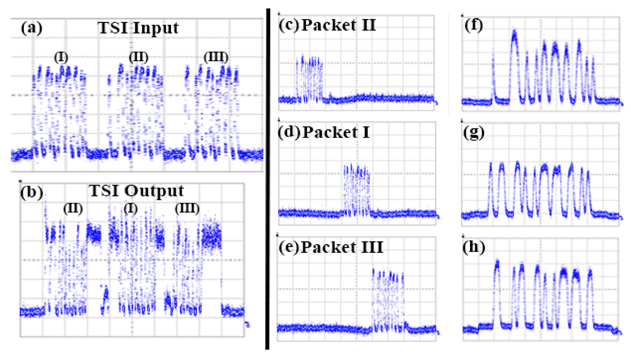
Figure 11 depicts the oscilloscope traces obtained when operating in Scenario 1 configuration, with Figure 11a showing the incoming data packets. Packet I was then converted to λ1 at WC1 to get a delay of 2Δτ, packet III was converted to λ2 and delayed then by Δτ, while packet II was converted to λ3 acquiring a zero-time slot delay. The resulting (II)-(I)-(III) ordered packet stream obtained at the Delay Stage output is depicted in Figure 11b, validating correct packet re-arrangement. The output traces of every individual packet at WC2 output are shown in Figure 11c–e, with respective zoomed-in versions shown in Figure 11f–h for each output packet, revealing the regenerative properties of the WC2 stage.
Figure 12 depicts the oscilloscope traces obtained to validate the TSI operation for Scenario 2, with Figure 12a depicting the incoming packet signal. In this case, packet (II) was converted to λ1 to acquire a 2Δτ delay, packet (I) was converted to λ2 and delayed then by Δτ, while packet (III) was converted to λ3 for direct transit. In this way, the resulting optical stream at the Delay Stage output had a packet order of (I)-(III)-(II) as shown in Figure 12b. The individual packets obtained at WC2 output are presented in Figure 12c–e with their respective zoomed-in versions illustrated in Figure 12f–h.
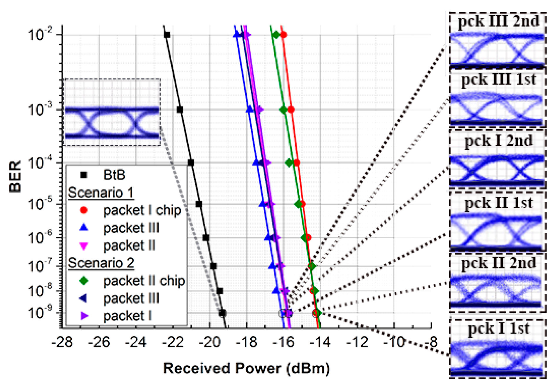
BER measurements were performed for every output packet in both TSI scenarios and are illustrated in Figure 13 along with the corresponding eye diagrams. Error-free operation at 10−9 was obtained for all packets with an average power penalty of 3 dB for the packets traversing the fiber-based delay lines and 5 dB for the packets traversing the integrated SOI-spiral waveguide. This higher power penalty is due to the noise that originates from the SOA amplification prior to chip coupling and is subsequently amplified in the EDFA.
4. Conclusions
In this paper, we are presenting our efforts towards the development of an optical packet router with advanced forwarding, buffering and packet rearrangement capabilities, while the packets remain in the optical domain. Our work is focusing on two subsystems with the first one demonstrating forwarding of optical packets encoded with BF-labels at 10 Gb/s, by utilizing a synergy between an FPGA control plane and a Si based 4 × 4 electro-optic switching matrix. The FPGA is performing all intensive logical operations i.e., BF-label extraction, membership checking and control signal generation that drive the MZIs of the 4 × 4 Si photonics matrix. The second proposed subsystem is relying on a Si chip with long spiral waveguides acting as integrated delay lines for the demonstration of optical buffering and optical TSI, for 10 Gb/s packets.
The BF-label packet forwarding concept is demonstrated successfully for 1 × 4 routing of incoming optical packets, while the look up forwarding table is updated every four packets. This rapid reconfiguration is extremely useful for fast changes in the network topology usually emerging from the virtualization of the hardware resources. The use of BF-encoded forwarding requires a number of look-up table entries that equals the number of switch outgoing ports, suggesting significant savings in router look-up table memory requirements, while the whole concept can easily be expanded to a larger scale. A single FPGA board can easily control more than 100 Si photonic switches, while large scale Si-pho switches have already been demonstrated in the literature [12,13,14,15,16].
The variable optical buffering and optical TSI stage is demonstrated for 10 Gb/s data packets with a Si chip featuring low loss spiral waveguides requiring a footprint of only 13.2 mm2 and a record-high delay versus footprint efficiency of 2.6 ns/mm2, while the delay path is defined by converting the incoming packets to the desired wavelength. All basic building blocks employed in our setup, including the SOI waveguide delays [51], the SOA-MZI WCs [19] and the AWGs [55] have been already shown as integrated modules on the same um-SOI platform. Additionally, utilizing the differentially biasing scheme, the SOA-MZI WCs have been successfully demonstrated to operate in cascaded stages [56] with up to 40 Gb/s NRZ data [57]. To this end, the proposed variable optical buffer and TSI circuits can be in principle implemented as integrated systems for contention resolution purposes operating with up to 40 Gb/s NRZ data.
Acknowledgments
This research has been partially supported by the EC H2020 project L3MATRIX (contract number 688544) and EC H2020 project ICT-STREAMS (contract number 688172).
Author Contributions
M.M.-P., G.M.-A., N.T. performed the experiments; N.T. programmed the FPGA controller; M.M.-P., N.T. and G.M.-A. prepared the manuscript while K.V. reviewed both the results and the manuscript.
Conflicts of Interest
The authors declare no conflict of interest.
References
- Di, S.; Kondo, D.; Cappello, F. Characterizing Cloud Applications on a Google Data Center. In Proceedings of the 42nd International Conference on Parallel Processing (ICPP), Lyon, France, 1–4 October 2013; pp. 468–473. [Google Scholar]
- Reiss, C.; Tumanov, A.; Ganger, G.R.; Katz, R.H.; Kozuch, M.A. Heterogeneity and dynamicity of clouds at scale: Google trace analysis. In Proceedings of the Third ACM Symposium on Cloud Computing, San Jose, CA, USA, 14–17 October 2012; pp. 1–13. [Google Scholar]
- Facebook. The Open Compute Server Architecture Specications. Available online: www.opencompute.org (accessed on 1 November 2017).
- Intel. Rack Scale Architecture. Available online: http://www.intel.com/content/www/us/en/architecture-and-technology/rack-scale-design-overview.html (accessed on 1 November 2017).
- Weiss, J.; Dangel, R.; Hofrichter, J.; Horst, F.; Jubin, D.; Meier, N.; La Porta, A.; Jan Offrein, B. Optical Interconnects for Disaggregated Resources in Future Datacenters; European Conference on Optical Communication (ECOC): Cannes, France, 2014; pp. 1–3. [Google Scholar]
- Ali, H.M.M.; Lawey, A.Q.; El-Gorashi, T.E.H.; Elmirghani, J.M.H. Energy efficient disaggregated servers for future data centers. In Proceedings of the 20th European Conference on Networks and Optical Communications—(NOC), London, UK, 30 June–2 July 2015; pp. 1–6. [Google Scholar]
- Papaioannou, A.D.; Nejabati, R.; Simeonidou, D. The Benefits of a Disaggregated Data Centre: A Resource Allocation Approach. In Proceedings of the IEEE Global Communications Conference (GLOBECOM), Washington, DC, USA, 4–8 December 2016; pp. 1–7. [Google Scholar]
- Available online: http://www.brocade.com/content/html/en/solution-design-guide/brocade-dc-fabric-architectures-sdg/GUID-A0E2AF7F-C47A-458D-989A-35EC97E262DD.html (accessed on 1 November 2017).
- Yu, M.; Fabrikant, A.; Rexford, J. BUFFALO: Bloom filter forwarding architecture for large organizations. In Proceedings of the 5th International Conference on Emerging Networking Experiments and Technologies, Rome, Italy, 1–4 December 2009; pp. 313–324. [Google Scholar]
- Li, D.; Li, Y.; Wu, J.; Su, S.; Yu, J. ESM: Efficient and Scalable Data Center Multicast Routing. IEEE/ACM Trans. Netw. 2012, 20, 944–955. [Google Scholar] [CrossRef]
- Rothenberg, C.E.; Macapuna, C.; Verdi, F.; Magalhães, M.; Zahemszky, A. Data center networking with in-packet Bloom filters. In Proceedings of the SBRC, Gramado, Brazil, 24 May 2010; pp. 553–566. [Google Scholar]
- Qiao, L.; Tang, W.; Chu, T. Ultra-large-scale silicon optical switches. In Proceedings of the IEEE 13th International Conference on Group IV Photonics (GFP), Shanghai, China, 24–26 August 2016; pp. 1–2. [Google Scholar]
- Seok, T.J.; Quack, N.; Han, S.; Muller, R.S.; Wu, M.C. Large-scale broadband digital silicon photonic switches with vertical adiabatic couplers. Optica 2016, 3, 64–70. [Google Scholar] [CrossRef]
- Suzuki, K.; Tanizawa, K.; Matsukawa, T.; Cong, G.; Kim, S.-H.; Suda, S.; Ohno, M.; Chiba, T.; Takadoro, H.; Yanagihara, M.; et al. Ultra-compact 8 × 8 strictly-non-blocking Si-wire PILOSS switch. Opt. Express 2014, 22, 3887–3894. [Google Scholar] [CrossRef] [PubMed]
- Chen, C.P.; Zhu, X.; Liu, Y.; Wen, K.; Chik, M.S.; Baehr-Jones, T.; Hochberg, M.; Bergman, K. Programmable Dynamically-Controlled Silicon Photonic Switch Fabric. J. Lightwave Technol. 2016, 34, 2952–2958. [Google Scholar] [CrossRef]
- Dupuis, N.; Rylyakov, A.V.; Schow, C.L.; Kuchta, D.M.; Baks, C.W.; Orcutt, J.S.; Gill, M.D.; Green, W.; Lee, B. Nanosecond-Scale Mach-Zehnder-Based CMOS Photonic Switch Fabrics. J. Lightwave Technol. 2017, 35, 615–623. [Google Scholar] [CrossRef]
- Nikolova, D.; Calhoun, D.M.; Liu, Y.; Rumley, S.; Novack, A.; Baehr-Jones, T.; Hochberg, M.; Bergman, K. Modular architecture for fully non-blocking silicon photonic switch fabric. Microsyst. Nanoeng. 2017, 3, 16071. [Google Scholar] [CrossRef]
- Shiraishi, T.; Li, Q.; Liu, Y.; Zhu, X.; Padmaraju, K.; Ding, R.; Hochberg, M.; Bergman, K. A Reconfigurable and Redundant Optically-Connected Memory System using a Silicon Photonic Switch. In Proceedings of the Optical Fiber Communication Conference, San Francisco, CA, USA, 9–13 March 2014; p. Th2A.10. [Google Scholar]
- Xiong, Y.; de Magalhães, F.G.; Radi, B.; Nicolescu, G.; Hessel, F.; Liboiron-ladouceur, O. Towards a Fast Centralized Controller for Integrated Silicon Photonic Multistage MZI-based Switches. In Proceedings of the Optical Fiber Communication Conference, Anaheim, CA, USA, 20–22 March 2016; p. W1J.2. [Google Scholar]
- Calhoun, D.; Wen, K.; Zhu, X.; Rumley, S.; Luo, L.; Liu, Y.; Ding, R.; Baehr-Jones, T.; Hochberg, M.; Lipson, M.; Bergman, K. Dynamic reconfiguration of silicon photonic circuit switched interconnection networks. In Proceedings of the IEEE High Perform Extreme Computer Conference, Waltham, MA, USA, 9–11 September 2014. [Google Scholar]
- Lou, F.; Fard, M.M.P.; Liao, P.; Hai, M.S.; Priti, R.; Huangfu, Y.; Qui, C.; Hao, Q.; Wei, Z.; Liboiron-Ladouceur, O. Towards a centralized controller for silicon photonic MZI-based interconnects. In Proceedings of the IEEE Optical Interconnects Conference (OI), San Diego, CA, USA, 20–22 April 2015; pp. 146–147. [Google Scholar]
- Calhoun, D.M.; Li, Q.; Browning, C.; Abrams, N.C.; Liu, Y.; Ding, R.; Barry, L.; Baehr-Jones, T.; Hochberg, M.; Bergman, K. Programmable wavelength locking and routing in a silicon-photonic interconnection network implementation. In Proceedings of the 2015 Optical Fiber Communications Conference and Exhibition (OFC), Los Angeles, CA, USA, 22–26 March 2015; pp. 1–3. [Google Scholar]
- Yiannopoulos, K.; Vlachos, K.G.; Varvarigos, E. Multiple-Input-Buffer and Shared-Buffer Architectures for Optical Packet- and Burst-Switching Networks. J. Lightwave Technol. 2007, 25, 1379–1389. [Google Scholar] [CrossRef]
- Miao, W.; Yan, F.; Calabretta, N. Towards Petabit/s All-Optical Flat Data Center Networks Based on WDM Optical Cross-Connect Switches with Flow Control. J. Lightwave Technol. 2016, 34, 4066–4075. [Google Scholar] [CrossRef]
- Terzenidis, N.; Moralis-Pegios, M.; Vagionas, C.; Pitris, S.; Chatzianagnostou, E.; Maniotis, P.; Syrivelis, D.; Tassiulas, L.; Miliou, A.; Pleros, N.; et al. Optically-Enabled Bloom Filter Label Forwarding Using a Silicon Photonic Switching Matrix. J. Lightwave Technol. 2017, 35, 4758–4765. [Google Scholar] [CrossRef]
- Moralis-Pegios, M.; Mourgias-Alexandris, G.; Terzenidis, N.; Cherchi, M.; Harjanne, M.; Aalto, T.; Miliou, A.; Pleros, N.; Vyrsokinos, K. On-chip SOI Delay Line Bank for Optical Buffers and Time Slot Interchangers. IEEE Photonics Technol. Lett. 2018, 30, 31–34. [Google Scholar] [CrossRef]
- Morichetti, F.; Melloni, A.; Ferrari, C.; Martinelli, M. Error-free continuously-tunable delay at 10 Gbit/s in a reconfigurable on-chip delay-line. Opt. Exp. 2008, 16, 8395–8405. [Google Scholar] [CrossRef]
- Kwack, M.J.; Oyama, T.; Hashizume, Y.; Mino, S.; Zaitsu, M.; Tanemura, T.; Nakano, Y. Integrated Optical Buffer Using InP 1 × 8 Switch and Silica-Based Delay Line Circuit; OFC: Los Angeles, CA, USA, 2012; pp. 1–3. [Google Scholar]
- Lee, H.; Chen, T.; Li, J.; Painter, O.; Vahala, K.J. Ultra-low-loss optical delay line on a silicon chip. Nat. Commun. 2012, 3, 867. [Google Scholar] [CrossRef] [PubMed]
- Burmeister, E.F.; Mack, J.P.; Poulsen, H.N.; Mašanović, M.L.; Stamenic, B.; Blumenthal, D.J.; Bowers, J.E. Photonic integrated circuit optical buffer for packet-switched networks. Opt. Exp. 2009, 17, 6629–6635. [Google Scholar] [CrossRef]
- LeGrange, J.D.; Simsarian, J.E.; Bernasconi, P.; Neilson, D.T.; Buhl, L.L.; Gripp, J. Demonstration of an integrated buffer for an all-optical packet router. IEEE Photonics Technol. Lett. 2009, 21, 781–783. [Google Scholar] [CrossRef]
- Moreira, R.L.; Garcia, J.; Li, W.; Bauters, J.; Barton, J.S.; Heck, M.J.; Blumenthal, D.J. Integrated Ultra-Low-Loss 4-Bit Tunable Delay for Broadband Phased Array Antenna Applications. IEEE Photonics Technol. Lett. 2013, 25, 1165–1168. [Google Scholar] [CrossRef]
- Pan, Z.; Subbaraman, H.; Lin, X.; Li, Q.; Zhang, C.; Ling, T.; Jay Guo, L.; Chen, R. Reconfigurable thermo-optic polymer switch based true-time-delay network utilizing imprinting and inkjet printing. In Proceedings of the Confrence on Lasers and Electro-Optics (CLEO), San Jose, CA, USA, 10–15 May 2014; pp. 1–2. [Google Scholar]
- Stopinski, S.; Malinowski, M.; Piramidowicz, R.; Kleijn, E.; Smit, M.K.; Leijtens, X.J.M. Integrated Optical Delay Lines for Time-Division Multiplexers. IEEE Photonics Technol. Lett. 2013, 5, 7902109. [Google Scholar] [CrossRef]
- Bloom, B.H. Space/time trade-offs in hash coding with allowable errors. Commun. ACM 1970, 13, 422–426. [Google Scholar] [CrossRef]
- Broder, A.; Mitzenmacher, M. Network applications of bloom filters: A survey. Internet Math. 2004, 1, 485–509. [Google Scholar] [CrossRef]
- Syrivelis, D.; Parisis, G.; Trossen, D.; Flegkas, P.; Sourlas, V.; Korakis, T.; Tassiulas, L. Pursuing a Software Defined Information-centric Network. In Proceedings of the European Workshop on Software Defined Networking, Darmstadt, Germany, 25–26 October 2012; pp. 103–108. [Google Scholar]
- You, W.; Mathieu, B.; Truong, P.; Peltier, J.F.; Simon, G. DiPIT: A Distributed Bloom-Filter Based PIT Table for CCN Nodes. In Proceedings of the 21st International Conference on Computer Communications and Networks (ICCCN), München, Germany, 30 July–2 August 2012; pp. 1–7. [Google Scholar]
- Du, Y.; He, G.; Yu, D. Efficient Hashing Technique Based on Bloom Filter for High-Speed Network. In Proceedings of the 8th International Conference on Intelligent Human-Machine Systems and Cybernetics (IHMSC), Hangzhou, China, 27–28 August 2016; pp. 58–63. [Google Scholar]
- Vyrsokinos, K.; Moralis-Pegios, M.; Vagionas, C.; Brimont, A.; Zanzi, A.; Sanchis, P.; Marti, J.; Kraft, J.; Rochracher, K.; Dorrestein, S.; et al. Single Mode Optical Interconnects for future data centers. In Proceedings of the 2016 18th International Conference on Transparent Optical Networks (ICTON), Trento, Italy, 10–14 July 2016; pp. 1–4. [Google Scholar]
- Xiong, Y.; Magalhães, F.G.D.; Nicolescu, G.; Hessel, F.; Liboiron-Ladouceur, O. Co-design of a low-latency centralized controller for silicon photonic multistage MZI-based switches. In Proceedings of the 2017 Optical Fiber Communications Conference and Exhibition (OFC), Los Angeles, CA, USA, 19–23 March 2017; pp. 1–3. [Google Scholar]
- T.I. Incorporated. LM7171 Datasheet. Available online: http://www.ti.com/product/LM7171/datasheet (accessed on 1 November 2017).
- Celo, D.; Goodwill, D.J.; Jia, J.; Dumais, P.; Chunshu, Z.; Fei, Z.; Tu, X.; Zhang, C.; Yan, S.; He, J.; et al. 32 × 32 silicon photonic switch. In Proceedings of the 2016 21st OptoElectronics and Communications Conference (OECC) Held Jointly with 2016 International Conference on Photonics in Switching (PS), Niigata, Japan, 3–7 July 2016; pp. 1–3. [Google Scholar]
- Cheng, Q.; Wonfor, A.; Wei, J.L.; Penty, R.V.; White, I.H. Demonstration of the feasibility of large-port-count optical switching using a hybrid Mach-Zehnder interferometer-semiconductor optical amplifier switch module in a recirculating loop. Opt. Lett. 2014, 39, 5244–5247. [Google Scholar] [CrossRef] [PubMed]
- Dupuis, N.; Rylyakov, A.V.; Schow, C.L.; Kuchta, D.M.; Baks, C.W.; Orcutt, J.S.; Gill, M.D.; Green, W.; Lee, B.G. Ultralow crosstalk nanosecond-scale nested 2 × 2 Mach–Zehnder silicon photonic switch. Opt. Lett. 2016, 41, 3002–3005. [Google Scholar] [CrossRef] [PubMed]
- Pitris, S.; Vagionas, C.; Tekin, T.; Broeke, R.; Kanellos, G.T.; Pleros, N. WDM-enabled optical RAM at 5 Gb/s using a monolithic InP flip-flop chip. IEEE Photonics J. 2016, 8, 1–7. [Google Scholar] [CrossRef]
- Beheshti, N.; Burmeister, E.; Ganjali, Y.; Bowers, J.E.; Blumenthal, D.J.; McKeown, N. Optical Packet Buffers for Backbone Internet Routers. IEEE/ACM Trans. Netw. 2010, 18, 1599–1609. [Google Scholar] [CrossRef]
- Geldenhuys, R.; Van der Merwe, J.S.; Thakulsukanant, K.; Wang, Z.; Chi, N.; Yu, S. Contention resolution and variable length optical packet switching using the active vertical-coupler-based optical Crosspoint switch. Opt. Switch. Netw. 2011, 8, 86–92. [Google Scholar] [CrossRef]
- Zouraraki, O.; Yiannopoulos, K.; Zakynthinos, P.; Petrantonakis, D.; Varvarigos, E.; Poustie, A.; Maxwell, G.; Avramopoulos, H. Implementation of an all-optical time-slot-interchanger architecture. IEEE Photonics Technol. Lett. 2007, 19, 1307–1309. [Google Scholar] [CrossRef]
- Sheng, X.; Feng, Z.; Li, B. Experimental investigation of all-optical packet-level time slot assignment using two optical buffers cascaded. Appl. Opt. 2013, 52, 2917–2922. [Google Scholar] [CrossRef] [PubMed]
- Moralis-Pegios, M.; Terzenidis, N.; Mourgias-Alexandris, G.; Vyrsokinos, K.; Pleros, N. A Low-Latency High-Port Count Optical Switch with Optical Delay Line Buffering for Disaggregated Data Centers; SPIE: San Francisco, CA, USA, 29 January 2018; pp. 10538–10544. [Google Scholar]
- Cherchi, M.; Ylinen, S.; Harjanne, M.; Kapulainen, M.; Vehmas, T.; Aalto, T. Low-loss spiral waveguides with ultra-small footprint on a micron scale SOI platform. In Proceedings of the SPIE, San Francisco, CA, USA, 8 March 2014. [Google Scholar]
- Aalto, T.; Solehmainen, K.; Harjanne, M.; Kapulainen, M.; Heimala, P. Low-loss converters between optical silicon waveguides of different sizes and types. IEEE Photonics Technol. Lett. 2006, 18, 709–711. [Google Scholar] [CrossRef]
- Apostolopoulos, D.; Vyrsokinos, K.; Zakynthinos, P.; Pleros, N.; Avramopoulos, H. A SOA-MZI NRZ Wavelength Conversion Scheme With Enhanced 2R Regeneration Characteristics. IEEE Photonics Technol. Lett. 2009, 21, 1363–1365. [Google Scholar] [CrossRef]
- Aalto, T.; Solehmainen, K.; Harjanne, M.; Kapulainen, M.; Heimala, P. Silicon photonics for optical connectivity: Small footprint with large dimensions. In Proceedings of the 2015 IEEE OI, Optical Interconnects Conference (OI), San Diego, CA, USA, 20–22 April 2015; pp. 40–41. [Google Scholar]
- Apostolopoulos, D.; Klonidis, D.; Zakynthinos, P.; Vyrsokinos, K.; Pleros, N.; Tomkos, I.; Avramopoulos, H. Cascadability Performance Evaluation of a new NRZ SOA-MZI Wavelength Converter. IEEE Photonics Technol. Lett. 2009, 21, 1341–1343. [Google Scholar] [CrossRef]
- Spyropoulou, M.; Pleros, N.; Vyrsokinos, K.; Apostolopoulos, D.; Bougioukos, M.; Petrantonakis, D.; Miliou, A.; Avramopoulos, H. 40 Gb/s NRZ Wavelength Conversion using a Differentially-Biased SOA-MZI: Theory and Experiment. J. Lightwave Technol. 2011, 29, 1489–1499. [Google Scholar] [CrossRef]
Figure 1.
(a) Close: (a) Construction process of a Bloom filter containing three different data elements in two phases; (b) Inverse operation where a query for a single element (DATA#B) is performed in the BF.
Figure 1.
(a) Close: (a) Construction process of a Bloom filter containing three different data elements in two phases; (b) Inverse operation where a query for a single element (DATA#B) is performed in the BF.

Figure 2.
Schematic illustration of the concept (a) Data#B residing at Resource Pool#1 and (b) with Data#B having migrated to Resource Pool#1 and Data#F having been added in Resource Pool#1.
Figure 2.
Schematic illustration of the concept (a) Data#B residing at Resource Pool#1 and (b) with Data#B having migrated to Resource Pool#1 and Data#F having been added in Resource Pool#1.

Figure 3.
Experimental setup used for experimental validation of the proposed network scenario.

Figure 4.
(a) The 4 × 4 Benes switch architecture depicting in bold the switches that were used in the 1 × 4 programmable node demonstration; (b) Packaged SiP chip.
Figure 4.
(a) The 4 × 4 Benes switch architecture depicting in bold the switches that were used in the 1 × 4 programmable node demonstration; (b) Packaged SiP chip.

Figure 5.
Insertion Losses from any input to any output port for the 4 × 4 Si photonics switch.

Figure 6.
Optical trace when light is inserted in port#3 and a 200 MHZ electrical clock signal modulates a switch in its optical path. Push -pull configuration is used.
Figure 6.
Optical trace when light is inserted in port#3 and a 200 MHZ electrical clock signal modulates a switch in its optical path. Push -pull configuration is used.

Figure 7.
(a)Experimental packet trace results recorded with the oscilloscope for control signals and packets at output of the 4 × 4 switch (b) Bit Error Rate (BER) measurements of the signal at the output of the switch using the FPGA and the PPG for driving the phase shifters of the MZIs. In the legend, i stands for input and o stands for output.

Figure 8.
(a) Close up view of the Si chip (b) Experimental setup for the variable optical buffer.

Figure 9.
(a) Initial three data packets (b–d) packet (I) after being delayed on the three integrated Si-spiral (e) BER measurements.
Figure 9.
(a) Initial three data packets (b–d) packet (I) after being delayed on the three integrated Si-spiral (e) BER measurements.

Figure 10.
(a) Experimental Setup of the TSI (b) Scenarios of packet re-arrangement for three packet input stream.
Figure 10.
(a) Experimental Setup of the TSI (b) Scenarios of packet re-arrangement for three packet input stream.

Figure 11.
(a) TSI Input (b) TSI Output (c,f) Packet II at WC2 Out (d,g) Packet I at WC2 Out (e,h) Packet III at WC2 Out.
Figure 11.
(a) TSI Input (b) TSI Output (c,f) Packet II at WC2 Out (d,g) Packet I at WC2 Out (e,h) Packet III at WC2 Out.

Figure 12.
(a) TSI Input (b) TSI Output (c,f) Packet II at WC2 Out (d,g) Packet I at WC2 Out (e,h) Packet III at WC2 Out.
Figure 12.
(a) TSI Input (b) TSI Output (c,f) Packet II at WC2 Out (d,g) Packet I at WC2 Out (e,h) Packet III at WC2 Out.

Figure 13.
BER measurements and packet eye diagrams.


Table 1.
Optimum Biasing Conditions for each one of the MZIs PSs in CROSS or BAR state.
| S1 | S2 | S3 | S4 | S5 | S6 | |
|---|---|---|---|---|---|---|
| CROSS | 1.08 V (21 mA) | 0 V | 1.03 V (17 mA) | 0.98 V (11 mA) | 0.89 V (6 mA) | 1.18 V (36 mA) |
| BAR | 0.89 V (4 mA) | 1.02 V (16 mA) | 0 V | 0 V | 0 V | 0.9 V (7 mA) |
© 2018 by the authors. Licensee MDPI, Basel, Switzerland. This article is an open access article distributed under the terms and conditions of the Creative Commons Attribution (CC BY) license (http://creativecommons.org/licenses/by/4.0/).
Share and Cite
MDPI and ACS Style
Moralis-Pegios, M.; Terzenidis, N.; Mourgias-Alexandris, G.; Vyrsokinos, K. Silicon Photonics towards Disaggregation of Resources in Data Centers. Appl. Sci. 2018, 8, 83. https://doi.org/10.3390/app8010083
AMA Style
Moralis-Pegios M, Terzenidis N, Mourgias-Alexandris G, Vyrsokinos K. Silicon Photonics towards Disaggregation of Resources in Data Centers. Applied Sciences. 2018; 8(1):83. https://doi.org/10.3390/app8010083
Chicago/Turabian StyleMoralis-Pegios, Miltiadis, Nikolaos Terzenidis, George Mourgias-Alexandris, and Konstantinos Vyrsokinos. 2018. "Silicon Photonics towards Disaggregation of Resources in Data Centers" Applied Sciences 8, no. 1: 83. https://doi.org/10.3390/app8010083
Note that from the first issue of 2016, this journal uses article numbers instead of page numbers. See further details here.