P(VDF-TrFE) Film on PDMS Substrate for Energy Harvesting Applications
by
 ,
,
Soaram Kim
1,*, 
Itmenon Towfeeq
1,
Yongchang Dong
2,
Sean Gorman
1,
Apparao M. Rao
2 and
Goutam Koley
1 1
Holcombe Department of Electrical and Computer Engineering, Clemson University, Clemson, SC 29634, USA
2
Department of Physics and Astronomy and Clemson Nanomaterials Institute, Clemson University, Clemson, SC 29634, USA
*
Author to whom correspondence should be addressed.
Appl. Sci. 2018, 8(2), 213; https://doi.org/10.3390/app8020213
Submission received: 15 November 2017
/
Revised: 5 January 2018
/
Accepted: 29 January 2018
/
Published: 31 January 2018
(This article belongs to the Special Issue Piezoelectric Energy Harvesting: Materials, Devices and Application)
Abstract
:We have developed and demonstrated a highly flexible P(VDF-TrFE) film-based energy harvesting device on a PDMS substrate, avoiding any complex composites and patterned structures. The structural and electrical properties of the P(VDF-TrFE) film was investigated using multiple characterization techniques and an optimized film of 7 µm thickness was used for the energy harvesting application. The device, with Ti/Ni metal contacts, was driven by a shaker providing an acceleration of 1.75 g, and frequencies varying from 5 to 30 Hz. The energy harvesting performance of the final fabricated device was tested using the shaker, and resulted in a maximum output capacitor voltage of 4.4 V, which successfully powered a set of 27 LEDs after several minutes of charging.
1. Introduction
Energy harvesting devices have attracted immense research interest over the years due to the need for powering remote and unattended sensors, as well as low-power electronics [1,2,3]. Several different types of energy harvesting devices have been investigated over the past decade, of which electromagnetic, electrostatic, and piezoelectric ones have received the most attention [4,5,6]. Piezoelectric energy harvesting devices are especially attractive due to their compact size and easy scalability and manufacturability. Among them, flexible piezoelectric material-based energy harvesters offer the advantage of being used in implantable or wearable bio-electronic devices and sensors, combined with the other advantages of piezoelectric generators, including high energy density, low mechanical damping, and easy voltage rectification [7]. Thus, they find usage in many applications including biometrics, strain monitoring, and mobile devices. While inorganic piezoelectric materials such as ZnO [8,9], ZnSnO3 [10,11], and PZT [12,13] have been used extensively for harvesting energy, flexible piezoelectric materials such as poly(vinylidenefluoride-co-trifluoroethylene) P(VDF-TrFE) [14,15] have been investigated recently due to their high piezoelectric coefficient, flexibility, sensitivity, and mechanical durability. In addition, P(VDF-TrFE) is fully bio-compatible, making it suitable for energy harvesting applications when implanted. P(VDF-TrFE), which can be simply obtained by varying the molar ratio of TrFE in proportion to PVDF, offers several advantages compared to PVDF, including higher piezoelectric coefficient [16], better crystallinity, higher remnant polarization, and higher temperature stability [17,18].
Since P(VDF-TrFE) is a film with a thickness of several microns, typically a substrate is utilized as mechanical support. Among the substrates used, polydimethylsiloxane (PDMS) substrate has proven to be particularly useful because of advantages such as high elasticity, easy molding capability, and biocompatibility. The flexibility and bio-compatibility of the PDMS substrate make the energy harvester attractive for usage in implantable or wearable devices, i.e., monitoring and tracking intrinsic (such as muscle fatigue) and extrinsic (such as twisting and bending of limbs) human parameters as part of biomedical applications, and smart monitoring systems including temperature sensors or low power microprocessors. Lee et al. [19] fabricated a nanogenerator (NG) using P(VDF-TrFE) film (active material, 7 µm) and a patterned PDMS-CNT composite as the bottom electrode, demonstrating maximum output voltage and current of 1.4 V and 150 nA, respectively. Wang et al. [20] developed patterned PDMS-MWCNT composite-based P(VDF-TrFE) (active material, 85 µm) hybrid energy harvester, and demonstrated piezoelectric output voltage and current of 2.5 V and 2.5 µA, respectively. Han et al. [21] reported that patterned PDMS used as micro/nano dual scale can increase the surface roughness and provide more strain to the PVDF film (active material, 100 µm) enhancing its power generation capacity. The resulting output voltage and current density reported from their devices were 52.8 V and 20.75 µA/cm2, respectively. Ding et al. [22] developed PDMS/polyethylene terephthalate (PET)-based PVDF (active material, 5 µm) energy harvester, and the demonstrated output voltage and current were 150 mV and 4 nA, respectively. The output performance PVDF and P(VDF-TrFE) energy harvesters are shown in Table 1 [15,19,20,21,22,23,24].
In spite of their promise, PDMS-based composites (with other materials, such as CNT) or patterned structures, as reported earlier, pose several challenges, including complicated fabrication processes, low reproducibility, non-uniform output, difficulty in interfacing with active layers like the P(VDF-TrFE) matrix, and degradation of structures over long-term usage in strong vibrational environments. An additional issue with the structure of PDMS-based composites (i.e., PDMS/CNT) is that, due to their higher resistance, the output current and voltage are usually much lower, strongly degrading energy harvesting performance. In this study, we have developed a flexible P(VDF-TrFE) film-based energy harvesting device on a simple PDMS substrate, avoiding any complex composites and patterned structures, while demonstrating performance comparable to or higher than the other devices reported on PDMS substrate. We have utilized profilometer, optical microscope, Fourier transform infrared (FTIR) spectroscopy and X-ray diffraction (XRD) to investigate the thickness, surface and structural properties of the P(VDF-TrFE) film. A COMSOL simulation was also performed to determine the strain and estimate the device performance. A shaker was used to measure the performance of the device at various frequencies, and power a set of LEDs as a simple application.
2. Experimental Details
2.1. Fabrication of the Flexible Piezoelectric Energy Harvester
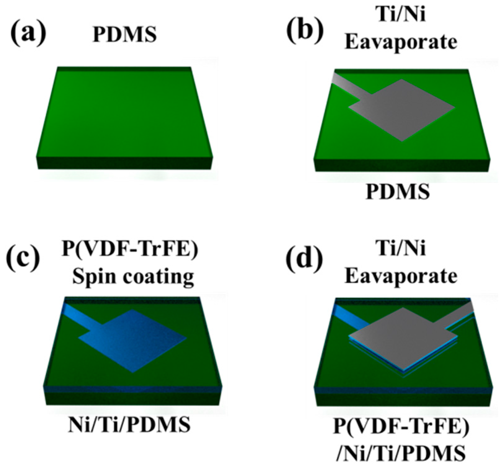
To fabricate the P(VDF-TrFE) films, first the co-polymer powder of P(VDF-TrFE) (50/50, Piezotech) was dissolved in N,N-dimethylformamide (DMF) solvent. The solution was then stirred for 12 h at 40 °C to synthesize 13 wt % of P(VDF-TrFE) solution. To make polydimethylsiloxane (PDMS) substrate (3.5 cm (W) × 3.5 cm (L) × 0.15 cm (H)), the liquid PDMS (weight ratio of elastomer to cross linker used was 10:1) was poured into square mold and then directly degassed to remove bubbles in a vacuum desiccator for 1 h. After that, it was heated in air at 100 °C for 30 min. Ti/Ni (30 nm/150 nm) metal stack (2 cm × 2 cm) was deposited at 100 °C by electron beam evaporation on the PDMS substrate to form the bottom electrode. Heat plays an important role in this fabrication process, as it improves the conductivity (by lowering resistance) when the Ti/Ni metal stack (2 cm × 2 cm) is deposited on the PDMS substrate directly. The PDMS substrate, owing to its tensile strength, was stretched while it was exposed to heat (100 °C), and first metal (Ti, 30 nm) was permeated into the surface of PDMS substrate, and then second metal (Ni, 150 nm) was finally deposited on the Ni/PDMS. Since cooling produces metal layer overlap, it makes the metal stack more stable under bending and vibration conditions from external force.
Next, a solution of the P(VDF-TrFE) was spin-coated on the PDMS substrate. A thickness of 7 µm was obtained by rotating the spin coater at 3500 rpm for 60 s. The DMF solvent was evaporated by pre-heating the device at 60 °C for 10 min. The film was subsequently heated in air at 140 °C for 2 h. A second layer of Ti/Ni (30 nm/150 nm) was deposited at 100 °C by electron beam evaporation to form the top electrode. To perform “poling” of the P(VDF-TrFE) film, an electric field of 100 MV/m was applied for 1 h to align the dipoles in the film [25]. The electric field of 100 MV/m was reached gradually by increasing the field by 10 MV/m in every 5 min to avoid breakdown due to sudden application of voltage. All the fabrication steps are shown in Figure 1.
2.2. Measurement and Characterization
The thickness, surface, and structural properties of the sample were investigated using profilometer (Tencor AS-200), optical microscopy (Micromanipulator Corp. MODEL No. 6000), Fourier transform infrared (FTIR) spectroscopy and X-ray diffraction (XRD). A shaker (LDS V203) was used to strain the P(VDF-TrFE) layer and a digital force gauge (Shimpo FG-3000) was used to measure the force from the shaker, which was converted to acceleration based on the mass moved. A digital phosphor oscilloscope (Tektronix TDS 5054), data acquisition (Agilent 34970A), and low-noise current preamplifier (Stanford Research Systems Model SR570) were used to measure the electrical signal from the device. In our experiment, the device was clamped to subject it to variable frequency excitation from the shaker attached with an extended arm, to investigate its performance (shown clearly in Figure 4a).
2.3. Simulations: Strain, Stress, and Potential
The strain and stress distribution on the P(VDF-TrFE) film was simulated using the COMSOL finite-element simulation software. A solid mechanics module was used to simulate the stress and deformation of the device. The Young’s Modulus used in the simulation was 2.3 × 10⁶ Pa for P(VDF-TrFE) and 2.6 × 10⁶ Pa for PDMS. The simulation used the same dimensions as in the fabricated device (3.5 × 3.5 cm for PDMS, and 2 × 2 cm for P(VDF-TrFE)), as shown in Figure 4b. An acceleration of 1.75 g was applied onto half of the bottom surface of this device. Considering PDMS comprises more than 99.9% of the thickness of the entire structure, the strain distribution is mainly dependent on PDMS layer. Hence the deformation of active material P(VDF-TrFE) can be assumed to be same as the deformation of the upper surface of the PDMS layer where it is attached. Since the edge of the shaker will first hit the center-line of the device, this point will experience the most strain during the process. When the shaker is in contact with the device, the active material experiences a uniform acceleration for a short period of time. Then strain is mainly formed within the stretched (overhanging) half of the device, as shown in Figure 4c. The potential simulation of COMSOL was performed using the information provided by the P(VDF-TrFE) powder manufacturer (Piezotech) with regard to the piezoelectric voltage constants g31, g32 and g33, which were 216, 19 and −339 × 10−3 Vm/Nm2, respectively. These results are shown in Figure 4d.
The resonance modes were investigated both analytically and through simulations. The fundamental resonant frequency (f0) of the device was found to be ~10.1 Hz from the equation:
where E is Young’s Modulus, ρ is density, t is thickness, w is width, and l is length. The resonant frequencies were also simulated using COMSOL, and f0, f1, and f2, turned out to be 11.77 Hz, 25.55 Hz, and 68.93 Hz, respectively. We excited the device at frequencies of 5, 10, 20 and 30 Hz, overlapping the range of frequency of fundamental and first order modes.
3. Results and Discussion
The schematic diagram of our flexible piezoelectric energy harvester is shown in Figure 2a. The device comprises four layers with the Ti/Ni as the top and bottom electrodes, the P(VDF-TrFE) piezoelectric film, and the PDMS substrate. Previously, a nanogenerator (NG) fabricated by Lee et al. [19] made use of the patterned PDMS-CNT composite to form the bottom electrode, while patterned PDMS was used as micro/nano dual scale by Han et al. [21] to increase the surface roughness of the NG. Wang et al. [20] also used patterned PDMS-MWCNT composite to obtain increased roughness and lower internal resistance in the device. As mentioned above, these methods included complex fabrication steps, such as chemical etching, photolithography, and plasma treatment, which add more cost and increase the complexity of fabrication. An optical image of our device, which is much simpler in construction, is shown in Figure 2b. All the materials, such as Ti/Ni for electrodes and P(VDF-TrFE) film for active area, were found to adhere well onto the PDMS substrate and withstand repeated cycles of bending and stretching.
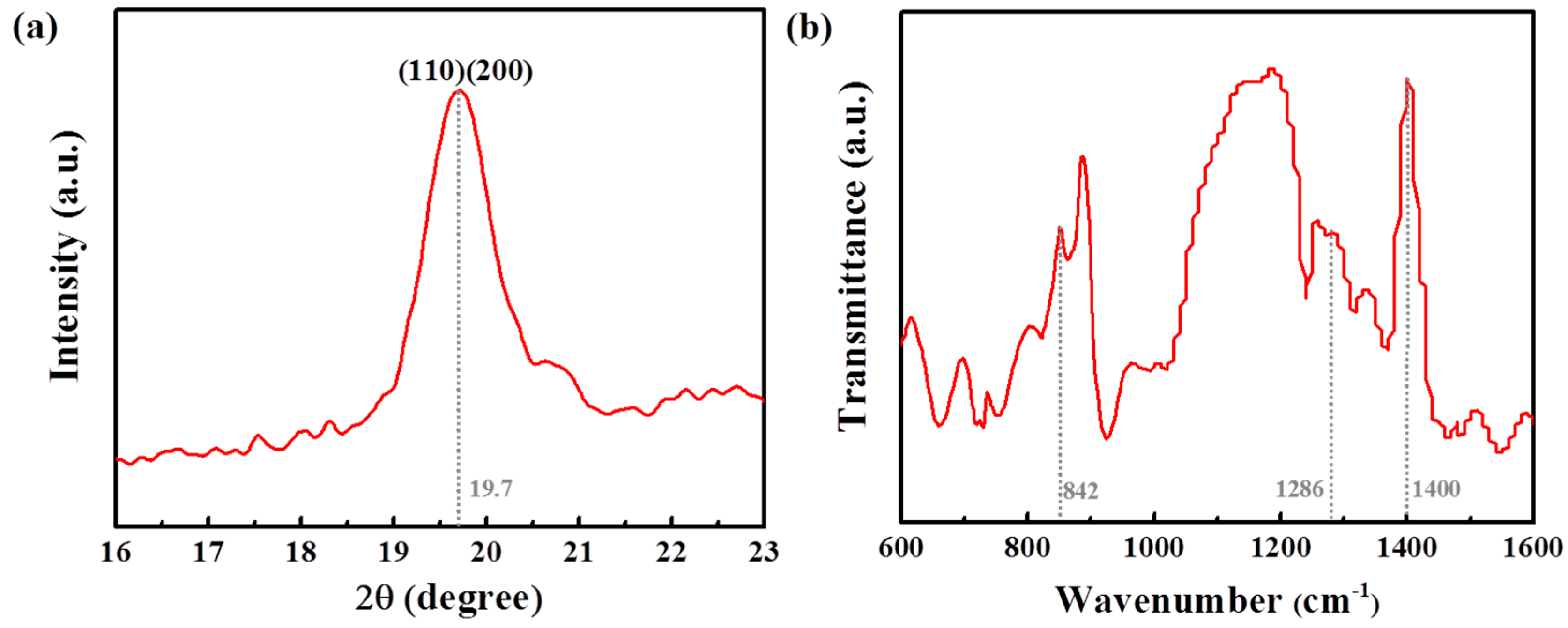
Once the composition and thickness had been optimized, we performed structural characterization using the XRD technique on the prepared P(VDF-TrFE) film, and the results are shown in Figure 3a. We found that the orientation planes (110) and (200) shown in the XRD spectra are related to the polar β-phase, since the diffraction peak position is shown at a 2θ value of 19.7° [26,27]. FTIR measurements were also carried out to further confirm the presence of β-phase P(VDF-TrFE). Figure 3b indicates the signature FTIR spectra of the film, with 3 peaks corresponding to the β-phase P(VDF-TrFE): 842 (CH2 rocking), 1286 (trans band) and 1400 (CH2 wagging) cm−1 [18,28]. Taken together, these tests clearly indicate that the synthesized film is indeed P(VDF-TrFE).
To determine the efficacy of the layered energy harvesting structure prepared, it was exposed to external strain using a mechanical shaker, and the output voltage and power were recorded. Figure 4a shows a photographic image of the basic experimental setup for energy harvesting, which consists of an oscilloscope (Tektronix TDS 5054), a Shaker (LDS V203), and the device attached to the shaker. The output voltages were obtained from the device under application of an external force at frequencies of 5, 10, 20 and 30 Hz at 1.75 g acceleration. The force was provided by the shaker. An extended metal arm from the shaker was attached to the bottom center of the device to provide the oscillatory force (see Figure 4a). The active area of the harvesting device is estimated to be ~4 cm2 (2 × 2 cm).
A COMSOL-based finite element simulation was performed to theoretically estimate the stress, strain, and voltage output from the device. From the simulation results (see Figure 4c) the peak and average stresses were found to be 8.42 × 10⁶ and 2.45 × 10⁶ N/m2, respectively, for the P(VDF-TrFE) films over the active area. The output voltage calculated from the relation V = g33 × σ3t (g33: piezoelectric voltage constant, σ3: applied mechanical stress, and t: thickness of film) yields the peak and average voltages of 20 and 5.8 V, respectively. Moreover, the peak and average surface charge densities of ~355 and 105 µC/m2 for 20 and 5.8 V, respectively, were obtained using the equation V = σt/ε (V: voltage, σ: surface charge density, t: thickness, and ε: dielectric constant). The calculated values of the voltages are well matched with the experimental data (see Figure 5), as well as simulation data for potential (see Figure 4d). The simulation figures show positive charge (and voltage) developing on the P(VDF-TrFE) positioned on top of the PDMS substrate, with negative charge and voltage at the interface of P(VDF-TrFE) and PDMS. The charges on the top surface of the P(VDF-TrFE) meet air, while the bottom surface has PDMS, so although the charge densities are the same, the voltage magnitudes generated are different.
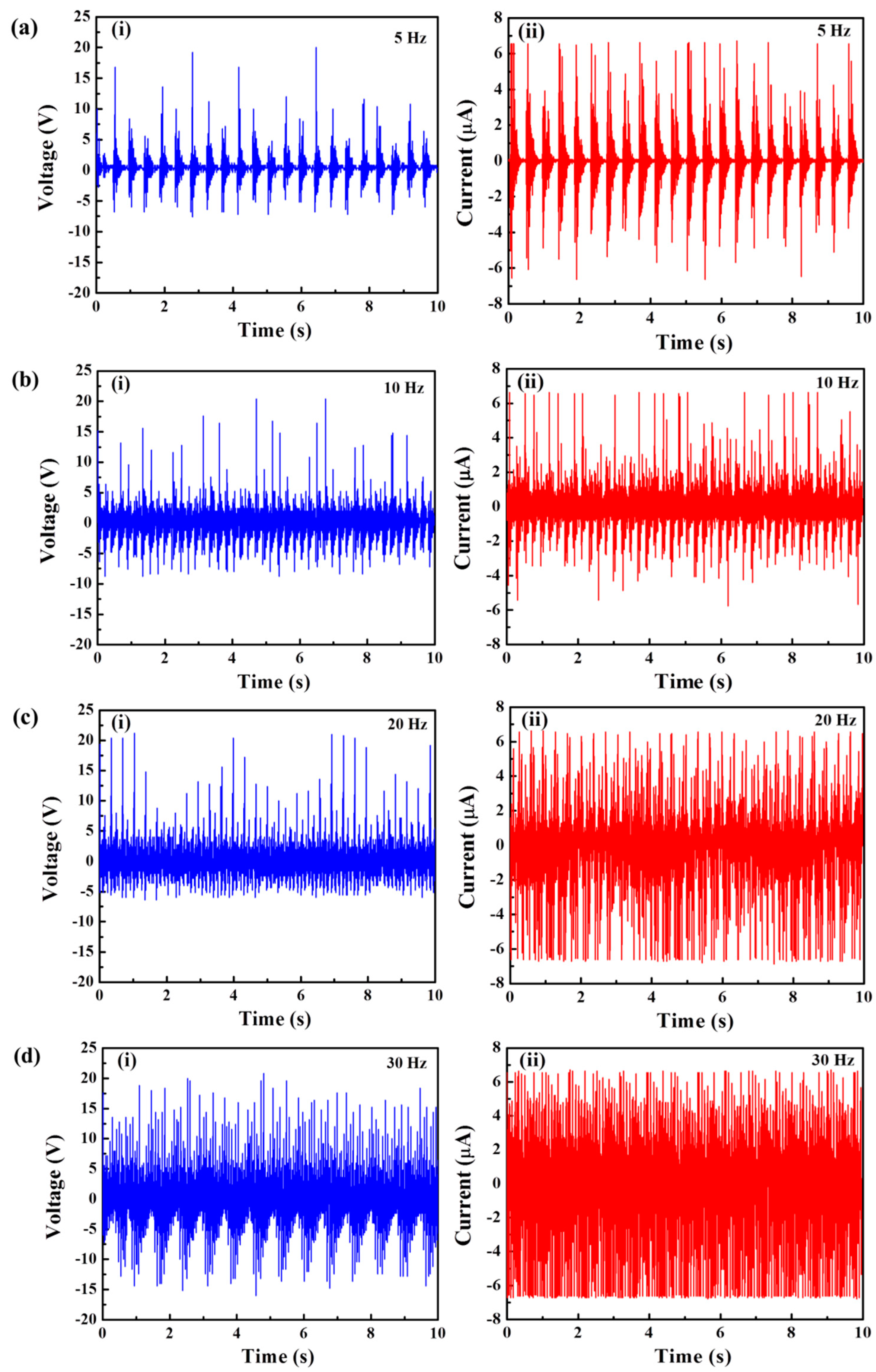
Figure 5a–d shows the frequency-dependent output voltage and current of the device under an external force at the various frequencies. The oscilloscope and low-noise current preamplifier were used to measure the electrical signal from the device. It is evident that the average voltage and current (solid parts of peaks in each figure) gradually increase with the increase of frequency, while the maximum upper peak voltage remains almost same at around 20 V. The increase in average voltage and current is attributed to the increase in the average surface charge as the bending frequency is increased. This occurs due to the slower discharge rate of the device as compared to the input pulse rate, resulting in a continuous rise in the output voltage and current as frequency is increased [29,30]. At 30 Hz, the peak value of average voltage and current is 5.8 V and 3.2 µA (see Table 2), while the maximum upper peak value of voltage and current is 20 V and 6.5 µA. These voltages are well matched with the calculated output potential, as mentioned above. Additionally, the value of average voltage of 5.8 V matches the final output voltage available across the full wave bridge rectifier circuit of 4.4 V (steady-state voltage value on the capacitor), considering a total drop across two diodes of ~1.4 V. This result is further discussed below.
The aforementioned energy harvesting performance is quite impressive, compared to the previously reported performance of flexible energy harvesters on PDMS substrate. Ding et al. [22] developed PDMS/PET-based PVDF (5 µm thick) piezoelectric NG with an output voltage of 150 mV. Wang et al. [20] fabricated patterned PDMS-MWCNT composite-based P(VDF-TrFE) (85 µm thick) hybrid NG, and piezoelectric output voltage was 2.5 V. Micropatterned (pyramid-shaped) P(VDF-TrFE) piezoelectric-pyroelectric NG (7 µm thick) on the CNT/PDMS composite substrate demonstrated by Lee et al. [19] led to an output voltage of only 1.4 V. By comparison, our device provides a significantly better performance, while requiring a much simpler fabrication process. Table 1 compares the output performance of the current device with various PVDF and P(VDF-TrFE) based NG reported earlier [15,19,20,21,22,23,24].
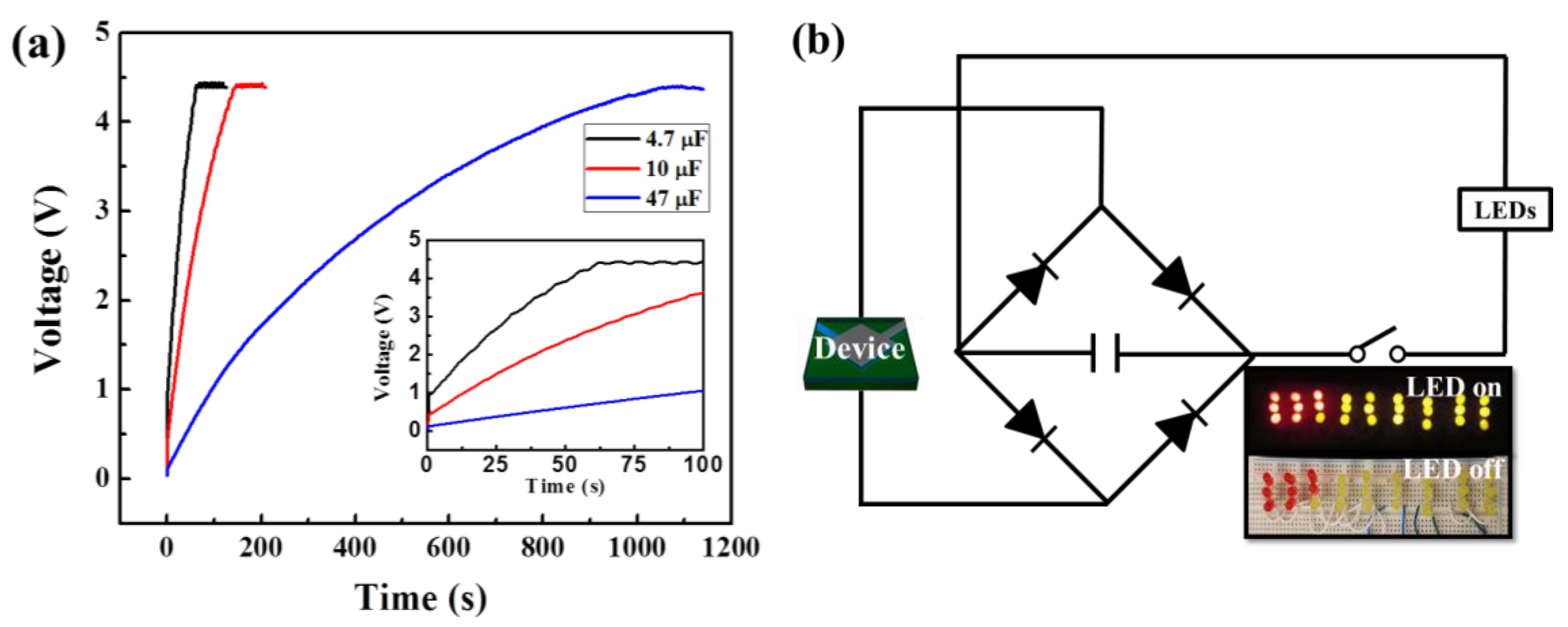
The output voltage transient across the output capacitors with different capacitance values of 4.7 µF, 10 µF, and 47 µF, under an external force with 30 Hz frequency, is shown in Figure 6a. The inset shows a magnified plot of charging transients up to 100 s. We found that the output voltage on the 4.7 µF capacitor terminals reached 4.4 V in ~60 s, while it took ~145 s and ~1085 s, respectively, to charge the 10 µF and 47 µF capacitors to the same voltage (4.4 V). The maximum stored energy and average power values were determined to be 113.74 µJ and 370 nW, respectively. Based on the active area and thickness of the sample (4 cm2 and 7 × 10⁻⁴ cm), the maximum output power density can be calculated as 6.62 mW/cm3, which is comparable to the state-of-the-art performance across all energy harvesting device technologies [5,15,19,20,21,22,23,24,31,32,33,34,35,36,37,38]. Although the power from the device is in the sub µW range, just a single device can still provide sufficient power to operate structural health monitoring devices, such as a 100 nW temperature sensor, or a low-power 4 kB 80 nW microprocessor [39,40,41].
To demonstrate a simple practical application of the energy harvester, we used it to light a set of 27 commercial LEDs connected in parallel. The overall circuit schematic, including 4 diodes, a switch, a capacitor, and 27 LEDs is shown in Figure 6b. As the capacitor reaches the threshold voltage (2.2 V), it turns on the LEDs, which then begin to glow. A picture of the lighted LEDs after the threshold voltage from the output capacitor was reached is shown in Figure 6b. This device can be used to charge many capacitors sequentially over a longer period to obtain a much higher stored energy that can be used for various applications, such as powering wireless sensors, wearable/implantable bio-electronic devices, or smart monitoring devices [42,43,44].
4. Conclusions
In this work, we have demonstrated a highly flexible, biocompatible PDMS-based piezoelectric energy harvester with P(VDF-TrFE) film utilizing a simple fabrication process. The device with an active area of 4 cm2 was found to have a power density of 6.62 mW/cm3 and average voltage and current of 5.8 V and 3.2 µA, respectively at 30 Hz vibration frequency at 1.75 g acceleration. Using a full wave bridge rectifier, a capacitor was charged and could deliver 370 nW, which was capable of lighting 27 LEDs simultaneously. With this power output, a wide range of wearable electronics and smart monitoring devices are within the realm of possible applications. In spite of the simple design, the performance of the present device was found to be superior compared to other flexible energy harvesters on PDMS substrate.
Acknowledgments
We thankfully acknowledge financial support for this work from the National Science Foundation through Grants# IIP-1512342, CBET-1606882 and IIP-1602006.
Author Contributions
This study was designed by Soaram Kim and Goutam Koley; Soaram Kim conducted the energy harvester layer-by-layer fabrication and all measurements, and wrote a major part of the paper under the supervision of Goutam Koley; Itmenon Towfeeq and Sean Gorman conducted design of charging circuit for the storage capacitor, and measurement of voltage and current, and analyzing output performances of the device with Soaram Kim; Yongchang Dong and Apparao M. Rao conducted COMSOL simulation and drawing schematic illustration of the device, and wrote simulations part of the paper; All authors contributed in revising the paper.
Conflicts of Interest
The authors declare no conflict of interest.
References
- Lee, J.-H.; Yoon, H.-J.; Kim, T.Y.; Gupta, M.K.; Lee, J.H.; Seung, W.; Ryu, H.; Kim, S.-W. Micropatterened P(VDF-TrFE) film-based piezoelectric nanogenerators for highly sensitive self-powered pressure sensors. Adv. Funct. Mater. 2015, 25, 3203–3209. [Google Scholar] [CrossRef]
- Hwang, G.-T.; Park, H.; Lee, J.-H.; Oh, S.; Park, K.-I.; Byun, M.; Park, H.; Ahn, G.; Jeong, C.K.; No, K.; et al. Self-powered cardiac pacemaker enable by flexible single crystalline PMN-PT piezoelectric energy harvester. Adv. Mater. 2014, 26, 4880–4887. [Google Scholar] [CrossRef] [PubMed]
- Gafforelli, G.; Corigliano, A.; Xu, R.; Kim, S.-G. Experimental verification of a bridge-shaped, nonlinear vibration energy harvester. Appl. Phys. Lett. 2014, 105, 203901. [Google Scholar] [CrossRef]
- Soares dos Santos, M.P.; Ferreira, J.A.F.; Simoes, J.A.O.; Pascoal, R.; Torrao, J.; Xue, X.; Furlani, E.P. Magnetic levitation-based electromagnetic energy harvesting: A semi-analytical non-linear model for energy transduction. Sci. Rep. 2016, 6, 18579. [Google Scholar] [CrossRef] [PubMed]
- Tao, K.; Wu, J.; Tang, L.; Hu, L.; Lye, S.W.; Miao, J. Enhanced electrostatic vibrational energy harvesting using integrated opposite-charged electrets. J. Micromech. Microeng. 2017, 27, 044002. [Google Scholar] [CrossRef]
- Alluri, N.R.; Selvarajan, S.; Chandrasekhar, A.; Saravanakumar, B.; Lee, G.M.; Jeong, J.H.; Kim, S.-J. Worm structure piezoelectric energy harvester using ionotropic gelation of barium titanate-clacium alginate composite. Energy 2017, 118, 1146–1155. [Google Scholar] [CrossRef]
- Khan, F.U.; Qadir, M.U. State-of-the-art in vibration-based electrostatic energy harvesting. J. Micromech. Microeng. 2016, 26, 103001. [Google Scholar] [CrossRef]
- Kim, D.Y.; Lee, S.; Lin, Z.-H.; Choi, K.H.; Doo, S.G.; Chang, H.; Leem, J.-Y.; Wang, Z.L.; Kim, S.-O. High temperature processed ZnO nanorods using flexible and transparent mica substrates for dye-sensitized solar cells and piezoelectric nanogenerators. Nano Energy 2014, 9, 101–111. [Google Scholar] [CrossRef]
- Chen, C.Y.; Huang, J.H.; Zhou, Y.; Lin, L.; Huang, P.C.; Liu, C.P.; He, J.H.; Wang, Z.L. Anisotropic outputs of a nanogeneator from oblique-aligned ZnO nanowire arrays. ACS Nano 2011, 5, 6707–6713. [Google Scholar] [CrossRef] [PubMed]
- Lee, K.Y.; Kim, D.; Lee, J.-H.; Kim, T.Y.; Gupta, M.J.; Kim, S.-W. Unidirectional high-power generation via stress-induced dipole alignment from ZnSnO3 nanocubes/polymer hybrid piezoelectric nanogenerator. Adv. Funct. Mater. 2014, 24, 37–43. [Google Scholar] [CrossRef]
- Wu, J.M.; Xu, C.; Zhang, Y.; Wang, Z.L. Lead-free nanogeneator made from single ZnSnO3 microbelt. ACS Nano 2012, 6, 4335–4340. [Google Scholar] [CrossRef] [PubMed]
- Park, K.-I.; Son, J.H.; Hwang, G.-T.; Jeong, C.K.; Ryu, J.; Koo, M.; Choi, I.; Lee, S.H.; Byun, M.; Wang, Z.L.; et al. Highly-efficient, flexible piezoelectric PZT thin film nanogenerator on plastic substrates. Adv. Mater. 2014, 26, 2514–2520. [Google Scholar] [CrossRef] [PubMed]
- Chen, X.; Xu, S.; Yao, N.; Shi, Y. Nanogenerator for mechanical energy harvesting using PZT nanofibers. Nano Lett. 2010, 10, 2133–2137. [Google Scholar] [CrossRef] [PubMed]
- Lee, J.-H.; Ryu, H.; Kim, T.-Y.; Kwak, S.-S.; Yoon, H.-J.; Kim, T.-H.; Seung, W.; Kim, S.-W. Thermally induced strain-coupled highly stretchable and sensitive pyroelectric nanognerators. Adv. Energy Mater. 2015, 5, 1500704. [Google Scholar] [CrossRef]
- Chen, X.; Tian, H.; Li, X.; Shao, J.; Ding, Y.; An, N.; Zhou, Y. A high performance P(VDF-TrFE) nanogenerator with self-connected and vertically integrated fibers by patterned EHD pulling. Nanoscale 2015, 7, 11536–11544. [Google Scholar] [CrossRef] [PubMed]
- Simoes, R.D.; Rodriguez-Perez, M.A.; Saja, J.A.D.; Constantino, C.J.L. Tailoring the structural properties of PVDF and P(VDF-TrFE) by using natural polymers as additives. Polym. Eng. Sci. 2009, 47, 2150–2157. [Google Scholar] [CrossRef]
- Ducrot, P.-H.; Dufour, I.; Ayela, C. Optimization of PVDF-TrFE processing conditions for the fabrication of organic MEMS resonators. Sci. Rep. 2016, 6, 19426. [Google Scholar] [CrossRef] [PubMed]
- Pi, Z.; Zhang, J.; Wen, C.; Zhang, Z.-B.; Wu, D. Flexible piezoelectric nanogenerator made of poly(vinylidenefluoride-co-trifluorethylene)(PVDF-TrFE) thin film. Nano Energy 2014, 7, 33–41. [Google Scholar] [CrossRef]
- Lee, J.-H.; Lee, K.Y.; Gupta, M.K.; Kim, T.Y.; Lee, D.-Y.; Oh, J.; Ryu, C.; Yoo, W.J.; Kang, C.-Y.; Yoon, S.-J.; et al. Highly stretchable piezoelectric-pyroelectric hybrid nanogenerator. Adv. Mater. 2014, 26, 765–769. [Google Scholar] [CrossRef] [PubMed]
- Wang, X.; Yang, B.; Liu, J.; Zhu, T.; Yang, C.; He, Q. A flexible triboelectric-piezoelectric hybrid nanogenrator based on P(VDF-TrFE) nanofibers and PDMS/MWCNT for wearable devices. Sci. Rep. 2016, 6, 36409. [Google Scholar] [CrossRef] [PubMed]
- Han, M.; Zhang, X.-S.; Meng, B.; Liu, W.; Tang, W.; Sun, X.; Wang, W.; Zhang, H. r-Shaped hybrid nanogenerator with enhanced piezoelectricity. ACS Nano 2013, 7, 8554–8560. [Google Scholar] [CrossRef] [PubMed]
- Ding, Y.; Duan, Y.; Huang, Y.A. Electrohydrohynamically printed, flexible energy harvester using in situ poled piezoelectric nanofibers. Energy Technol. 2015, 3, 351–358. [Google Scholar] [CrossRef]
- Liu, Z.; Zhang, S.; Jin, Y.M.; Ouyang, H.; Zou, Y.; Wang, X.X.; Xie, L.X.; Li, Z. Flexible piezoelectric nanogenerator in wearable self-powered active sensor for respiration and healthcare monitoring. Semicond. Sci. Technol. 2017, 32, 064004. [Google Scholar] [CrossRef]
- Bhavanasi, V.; Kumar, V.; Parida, K.; Wang, J.; Lee, P.S. Enhanced piezoelectric energy harvesting performance of flexible PVDF-TrFE bilayer films with graphene oxide. ACS Appl. Mater. Interfaces 2016, 8, 521–529. [Google Scholar] [CrossRef] [PubMed]
- Kim, S.; Towfeeq, I.; Bayram, F.; Khan, D.; Koley, G. Highly flexible P(VDF-TrFE) film-based piezoelectric self-powered energy harvester. In Proceedings of the IEEE Sensors, Orlando, FL, USA, 30 October–3 November 2016; pp. 1–3. [Google Scholar]
- Chen, S.; Yao, K.; Tay, F.E.H.; Chew, L.L.S. Comparative investigation of the structure and properties of ferroelectric poly(vinylidene fluoride) and poly(vinylidene fluoride-trifluoroethylene) thin films crystallized on substrates. J. Appl. Polym. Sci. 2010, 116, 3331–3337. [Google Scholar] [CrossRef]
- Paik, H.; Choi, Y.-Y.; Hong, S.; No, K. Effect of Ag nanoparticle concentration on the electrical and ferroelectric properties of Ag/P(VDF-TrFE) composite films. Sci. Rep. 2015, 5, 13209. [Google Scholar] [CrossRef] [PubMed]
- Ma, W.; Zhang, J.; Chen, S.; Wang, X. Crystalline phase formation of poly(vinylidenefluoride) from tetrahydrofuran/N,N-dimethylformamide mixed solutions. J. Macromol. Sci. B 2008, 47, 434–449. [Google Scholar] [CrossRef]
- Ko, Y.H.; Nagaraju, G.; Lee, S.H.; Yu, J.S. PDMS-based triboelectric and transparent nanogenerators with ZnO nanorod arrays. ACS Appl. Mater. Interfaces 2014, 6, 6631–6637. [Google Scholar] [CrossRef] [PubMed]
- Fan, F.-R.; Tian, Z.-Q.; Wang, Z.L. Flexible triboelectric generator! Nano Energy 2012, 1, 328–334. [Google Scholar] [CrossRef]
- Sinha, T.K.; Ghosh, S.K.; Maiti, R.; Jana, S.; Adhikari, B.; Mandal, D.; Ray, S.K. Graphene-silver-induced self-polarized PVDF-based flexible plasmonic nanogenerator toward the realization for new class of self powered optical sensor. ACS Appl. Mater. Interfaces 2016, 8, 14986–14993. [Google Scholar] [CrossRef] [PubMed]
- Kim, S.; Gupta, M.K.; Lee, K.Y.; Sohn, A.; Kim, T.Y.; Shin, K.-S.; Kim, D.; Kim, S.K.; Lee, K.H.; Shin, H.-J.; et al. Transparent flexible graphene triboelectric nanognerators. Adv. Mater. 2014, 26, 3918–3925. [Google Scholar] [CrossRef] [PubMed]
- Xiong, J.; Lin, M.-F.; Wang, J.; Gaw, S.L.; Parida, K.; Lee, P.S. Wearable all-fabric-based triboelectric generator for water energy harvesting. Adv. Energy Mater. 2017, 1701243, 1–10. [Google Scholar] [CrossRef]
- Moyet, R.P.; Stace, J.; Amin, A.; Finkel, P.; Rossetti, G.A. Non-resonant electromechanical energy harvesting using inter-ferroelectric phase transitions. Appl. Phys. Lett. 2015, 107. [Google Scholar]
- Bonisoli, E.; Repetto, M.; Manca, N.; Gasparini, A. Electromechanical and electronic integrated harvester for shoes application. IEEE/ASME Trans. Mech. 2017, 22, 1921–1932. [Google Scholar] [CrossRef]
- Takhedmit, H.; Saddi, Z.; Karami, A.; Basset, P.; Cirio, L. Electrostatic vibration energy harvester with 2.4-GHz cockcroft-walton rectenna start-up. C. R. Phys. 2017, 18, 98–106. [Google Scholar] [CrossRef]
- Liu, H.; Chen, T.; Sun, L.; Lee, C. An electromagnetic MEMS energy harvester array with multiple vibration modes. Micromachines 2015, 6, 984–992. [Google Scholar] [CrossRef]
- Roy, S.; Podder, P.; Mallick, D. Nonlinear energy harvesting using electromagnetic transduction for wide bandwidth. IEEE Magn. Lett. 2016, 7, 5701004. [Google Scholar] [CrossRef]
- Lee, Y.; Blaauw, D.; Sylvester, D. Ultralow power circuit design for wireless sensor nodes for structural health monitoring. Proc. IEEE 2016, 104, 1529–1546. [Google Scholar] [CrossRef]
- Jeong, S.; Foo, Z.; Lee, Y.; Sim, J.-Y.; Blaauw, D.; Sylvester, D. A fully-integrated 71 nW CMOS temperature sensor for low power wireless sensor nodes. IEEE J. Solid State Circuits 2014, 49, 1682–1693. [Google Scholar] [CrossRef]
- Lim, W.; Lee, I.; Sylvester, D.; Blaauw, D. Batteryless sub-nW cortex-MO+ processor with dynamic leakage-suppression logic. In Proceedings of the 2015 IEEE International Solid-State Circuits Conference, San Francisco, CA, USA, 22–26 February 2015. [Google Scholar] [CrossRef]
- Liu, X.; Zhu, Y.; Nomani, M.W.; Wen, X.; Hsia, T.Y.; Koley, G. A highly sensitive pressure sensor using a Au-patterned polydimethylsiloxane membrane for biosensing applications. J. Micromech. Microeng. 2013, 23, 025022. [Google Scholar] [CrossRef]
- Koley, G.; Liu, J.; Nomani, M.W.; Yim, M.; Wen, X.; Hsia, T.Y. Miniaturized implantable pressure and oxygen sensors based on polydimethylsiloxane thin films. Mater. Sci. Eng. C 2009, 29, 685–690. [Google Scholar] [CrossRef] [PubMed]
- Singh, A.; Uddin, M.A.; Sudarshan, T.; Koley, G. Tunable reverse-biased graphene/silicon heterojunction schottky diode sensor. Small 2014, 10, 1555–1565. [Google Scholar] [CrossRef] [PubMed]
Figure 1.
(a) PDMS substrate (3.5 cm (W) × 3.5 cm (L) × 0.15 cm (H)) was made by elastomer and cross linker (weight ratio 10:1); (b) Ti/Ni (30 nm/150 nm) was deposited on the PDMS substrate by electron beam evaporator; (c) P(VDF-TrFE) was spin-coated on Ni/Ti/PDMS at 3500 rpm for 60 s; (d) Ti/Ni (30 nm/150 nm) was deposited on the P(VDF-TrFE)/Ni/Ti/PDMS by electron beam evaporator. After that an electric field of 100 MV/m was applied for 1 h to align the dipoles in the P(VDF-TrFE) film uniformly.

Figure 2.
(a) Schematic illustration; (b) optical microscopy image; and (c) photographic image of the proposed device.
Figure 2.
(a) Schematic illustration; (b) optical microscopy image; and (c) photographic image of the proposed device.
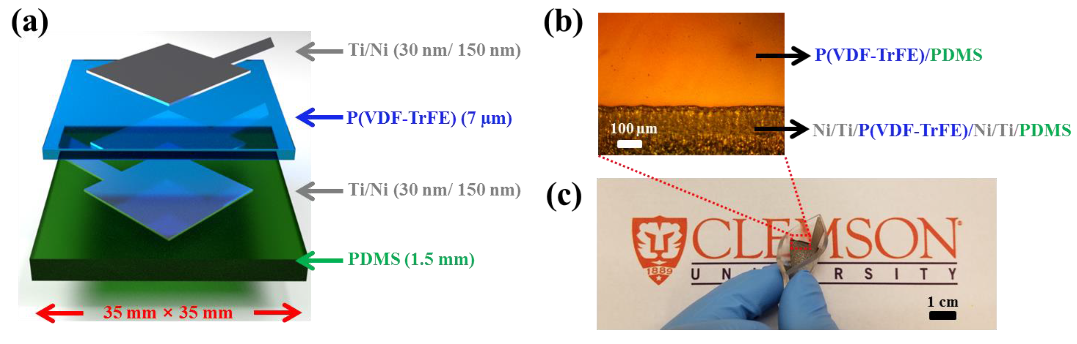
Figure 3.
(a) XRD and (b) FTIR result of β-phase of P(VDF-TrFE) film. The XRD peak at 19.7 degrees and the transmittance peaks at 842, 1286 and 1400 cm−1 confirm the material is β-phase P(VDF-TrFE).
Figure 3.
(a) XRD and (b) FTIR result of β-phase of P(VDF-TrFE) film. The XRD peak at 19.7 degrees and the transmittance peaks at 842, 1286 and 1400 cm−1 confirm the material is β-phase P(VDF-TrFE).

Figure 4.
(a) Photographic image of the basic experimental setup and (b) image of the device under test; (c) Finite element (COMSOL) simulation of strain and stress distribution and (d) piezoelectric output voltages and surface charge densities over the active area (2 × 2 cm2).
Figure 4.
(a) Photographic image of the basic experimental setup and (b) image of the device under test; (c) Finite element (COMSOL) simulation of strain and stress distribution and (d) piezoelectric output voltages and surface charge densities over the active area (2 × 2 cm2).
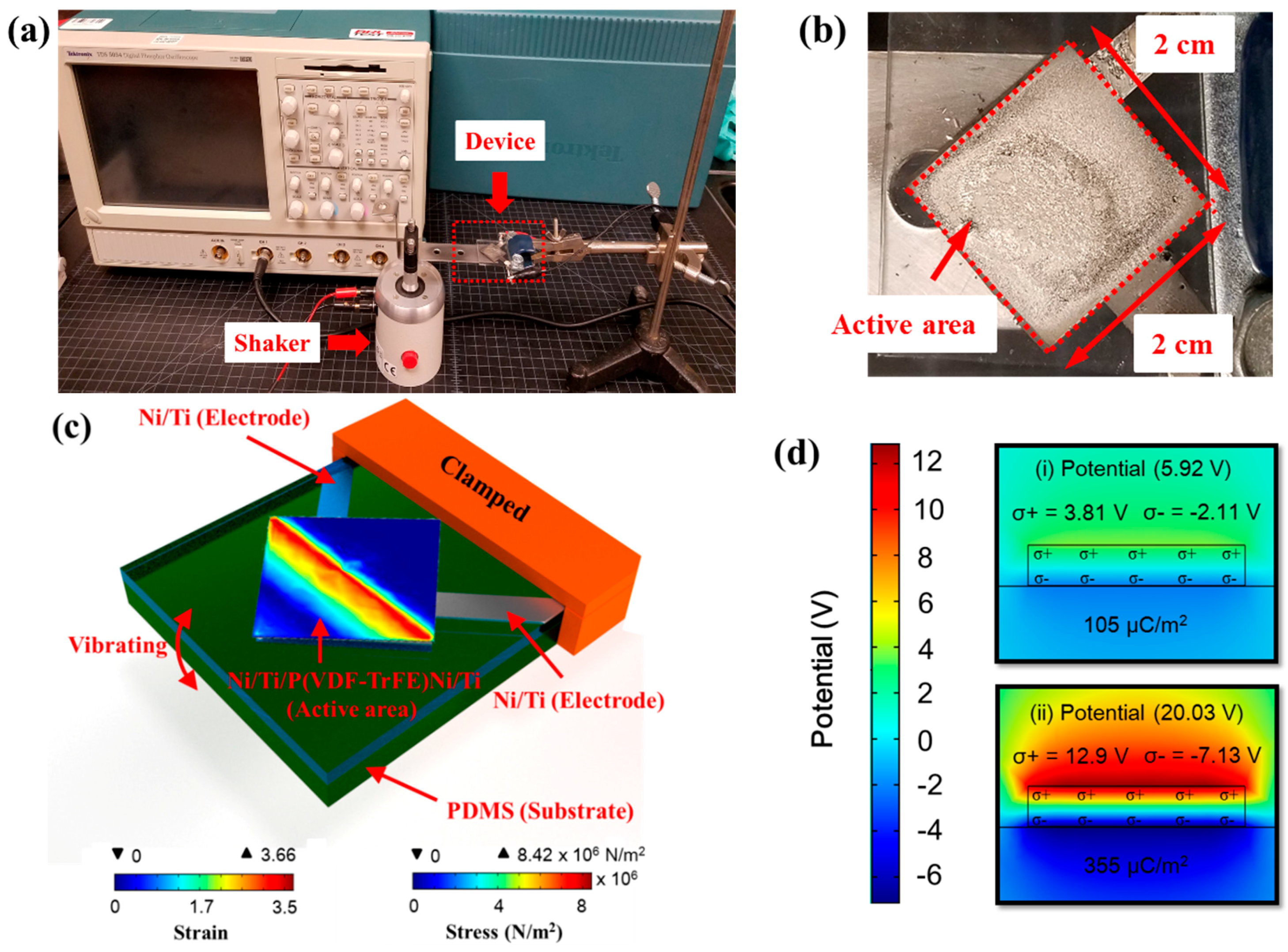
Figure 5.
(a–d) the frequency-dependent (5, 10, 20 and 30 Hz, respectively) output (i) voltage and (ii) current of the device under application of an external force.
Figure 5.
(a–d) the frequency-dependent (5, 10, 20 and 30 Hz, respectively) output (i) voltage and (ii) current of the device under application of an external force.

Figure 6.
(a) Voltage-time charging curve of storage capacitors with different capacitances (4.7 µF, 10 µF, and 47 µF) under application of an external force with 30 Hz frequency. The inset shows an enlarged plot of voltage-time charging curves; (b) Electric charging circuit for the storage capacitor, and a picture of an LED assembly that glows by drawing power from the storage capacitor after energy harvesting is done.


Table 1.
Comparison of the output performance of piezoelectric energy harvesters in recent years. The current work is shown in bold.
Table 1.
Comparison of the output performance of piezoelectric energy harvesters in recent years. The current work is shown in bold.
| Substrate | Piezoelectric Material (µm) | Size (cm2) | Output Performance | Input Frequency (Hz) | Reference | ||
|---|---|---|---|---|---|---|---|
| Voltage (V) | Current (µA) Current Density (µA/cm2) | Power Density (mW/cm3) | |||||
| PDMS | P(VDF-TrFE) (7 µm) | 2 × 2 | 5.8 V | 3.2 µA 0.8 µA/cm2 | 6.62 | 5~30 | This work |
| CNT/PDMS | P(VDF-TrFE) (7 µm) | 4 × 4 | 1.4 V | ~150 nA | 0.018 | N/A | [19] |
| MWCNT/PDMS | P(VDF-TrFE) (85 µm) | 0.8 × 0.8 | 2.5 V | ~2.5 µA | 0.689 | 1~4 | [20] |
| PDMS | PVDF (100 µm) | 4 × 2 | 52.8 V | 20.75 µA/cm2 | 10.95 | 5~10 | [21] |
| PDMS | PVDF (5 µm) | 3 × 3 | 150 mV | 4 nA | 1.33 × 10⁻⁴ | 1~2.3 | [22] |
| ITO | P(VDF-TrFE) (50 µm) | 1 × 1 | 4.0 V | 2.6 µA | 2.08 | 1~100 | [15] |
| Silicone | PVDF (200 µm) | 4.2 × 2 | 1.5 V | 400 nA | 3.57 × 10⁻³ | ~1.4 | [23] |
| N/A (ITO & Gold electrodes) | P(VDF-TrFE) (30 µm) | 1 × 1 | 4 V | 1.88 µA | 2.5 | 1 | [24] |
Table 2.
Average output voltage, current, and power of the device for various excitation frequencies.
Table 2.
Average output voltage, current, and power of the device for various excitation frequencies.
| Frequency (Hz) | Average Voltage (V) | Average Current (µA) | Average Power (µW) |
|---|---|---|---|
| 5 | 2.8 | 1.2 | 3.36 |
| 10 | 3.3 | 1.5 | 4.95 |
| 20 | 3.8 | 2.1 | 7.98 |
| 30 | 5.8 | 3.2 | 18.56 |
© 2018 by the authors. Licensee MDPI, Basel, Switzerland. This article is an open access article distributed under the terms and conditions of the Creative Commons Attribution (CC BY) license (http://creativecommons.org/licenses/by/4.0/).
Share and Cite
MDPI and ACS Style
Kim, S.; Towfeeq, I.; Dong, Y.; Gorman, S.; Rao, A.M.; Koley, G. P(VDF-TrFE) Film on PDMS Substrate for Energy Harvesting Applications. Appl. Sci. 2018, 8, 213. https://doi.org/10.3390/app8020213
AMA Style
Kim S, Towfeeq I, Dong Y, Gorman S, Rao AM, Koley G. P(VDF-TrFE) Film on PDMS Substrate for Energy Harvesting Applications. Applied Sciences. 2018; 8(2):213. https://doi.org/10.3390/app8020213
Chicago/Turabian StyleKim, Soaram, Itmenon Towfeeq, Yongchang Dong, Sean Gorman, Apparao M. Rao, and Goutam Koley. 2018. "P(VDF-TrFE) Film on PDMS Substrate for Energy Harvesting Applications" Applied Sciences 8, no. 2: 213. https://doi.org/10.3390/app8020213
Note that from the first issue of 2016, this journal uses article numbers instead of page numbers. See further details here.