Excitation of Wet Perovskite Films by Ultrasonic Vibration Improves the Device Performance


University of Michigan-Shanghai Jiao Tong University Joint Institute, Shanghai 200240, China
*
Author to whom correspondence should be addressed.
Appl. Sci. 2018, 8(2), 308; https://doi.org/10.3390/app8020308
Submission received: 8 February 2018
/
Revised: 17 February 2018
/
Accepted: 19 February 2018
/
Published: 21 February 2018
(This article belongs to the Section Acoustics and Vibrations)
Abstract
:In this work, a novel, facile, and low-cost mechanical post treatment technique, i.e., ultrasonic substrate vibration post treatment (SVPT) is applied on wet spun perovskite layers. The effect of varying the time of the SVPT on the characteristics of the perovskite crystals and the perovskite film is studied, in order to achieve the optimum time duration of the SVPT. Among the results, it is found that the application of only three minutes of the SVPT (for the ultrasonic vibration assembly used in this study, operated at 40 kHz) brings about significant improvement in the film coverage, and the contact between the perovskite and the m-TiO2 layers, owing to the effective penetration of the perovskite solution into the pores, leading to a superior charge transfer, and a significant increase in the device power conversion efficiency (PCE), when compared to the control device. This unprecedented effect is repeatable when applied on both single and mixed halide perovskites, putting forward a reliable and low-cost mechanical technique for the fabrication of perovskite solar cells (PSCs) in the lab and beyond, which could reduce or eliminate the tedious and expensive chemical optimization treatments, commonly used to increase the PCE.
1. Introduction
Perovskite solar cells (PSCs) are currently one of the most favorable and efficient types of emerging solution-processed thin film solar cells, owing to the excellent optoelectronic properties of the perovskite light harvesters [1,2,3], although the device instability under normal operation and the process scale-up, using low-cost fabrication routes, are two major challenges against the commercialization of this technology. PSCs may be designed as the p-i-n or n-i-p types, owing to the ambipolar behavior of the perovskite light harvesters. The basic and widely-studied n-i-p PSC is comprised of glass/TCO/c-TiO2/m-TiO2/perovskite/HTL/metal electrode, where the TCO stands for the transparent conducting oxides, such as fluorine-doped tin oxide (FTO), c-TiO2 denotes a compact film of TiO2, m-TiO2 denotes a mesoporous layer made of the TiO2 nanoparticles, and the HTL stands for the hole transporting layer. The c-TiO2 ultrathin layer plays the pivotal role of the electron transporting layer (ETL), whereas the HTL is made of a material that has the ability to transport the holes only, such as spiro-OMeTAD (2,2′,7,7′-Tetrakis [N,N-di(4-methoxyphenyl) amino]-9,9′-spirobifluorene). The m-TiO2 layer controls the growth and deposition of the perovskite nanocrystals within the pores of the mesoporous layer, but may be excluded in some designs, so as to simplify the fabrication process and reduce the cost. The heart of a lead halide methylammonium PSC has the formulation of methylammonium lead halide, CH3NH3PbX3 (MAPbX3), where X = I, Br or Cl or any combination thereof [4]. Beside the MA-based PSCs, formamidinium (FA) and Cs based PSCs have been developed, in order to improve the device performance and stability [5,6]. As a model system, this fundamental work adopts the basic mesoporous structure (c-TiO2/m-TiO2) [7] with MA as the cation and both single and mixed halides in the perovskite layer for further investigation and the optimization of the deposition process of the perovskite layer atop the mesoporous layer, using a novel ultrasonic vibration technique to be elaborated upon later on.
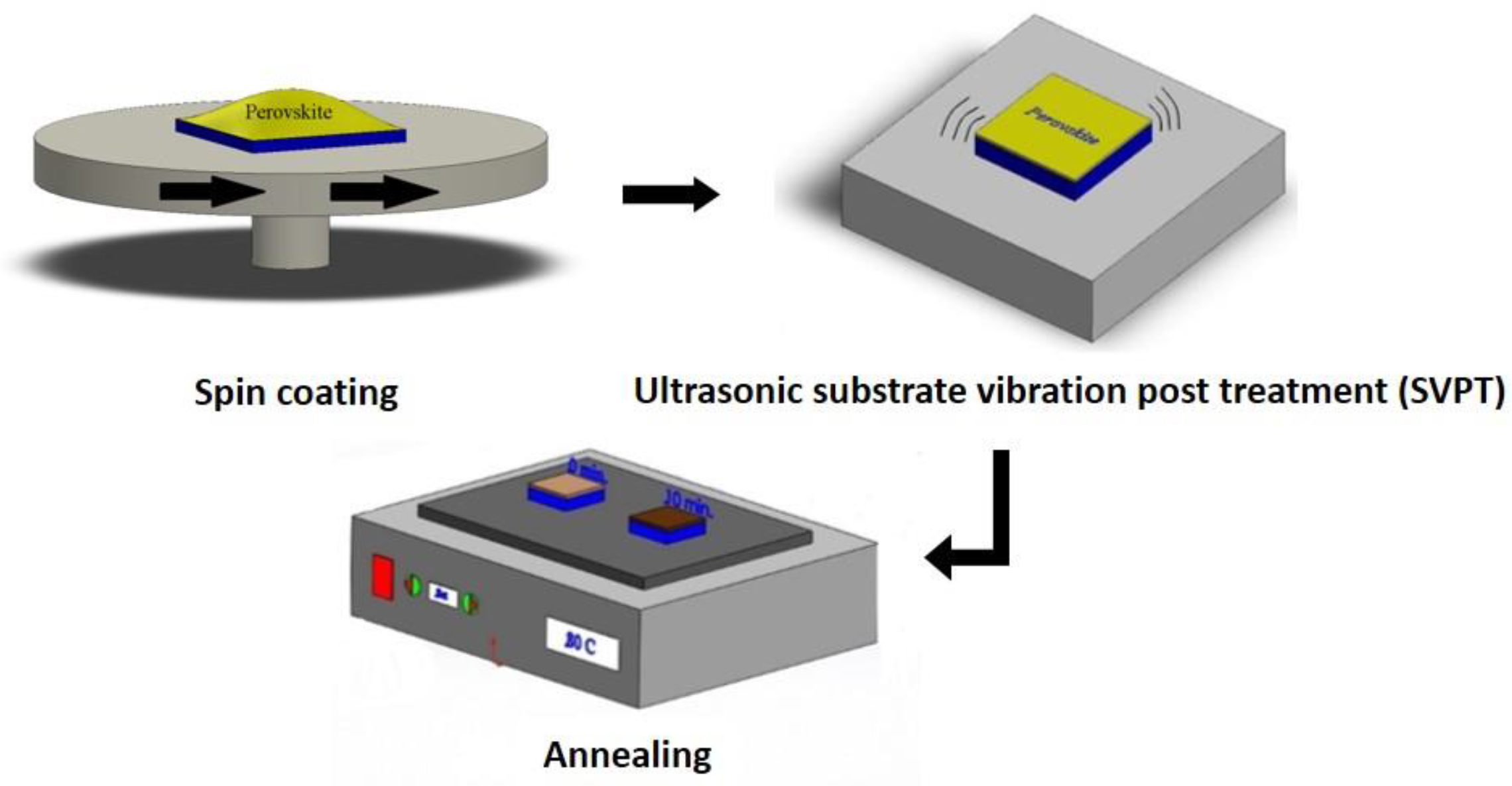
To prepare the perovskite layer, the precursors such as lead halides and methylammonium halides may be mixed and deposited directly from solution in one-step, or separately deposited in two sequential steps for better coverage, at the expense of additional steps and cost. Therefore, the one-step method is easier to perform and is in line with the scale-up of the technology, and therefore adopted in this work. Regardless of the method of deposition, the perovskite crystallization process is usually controlled by cooling/heating and/or solvent engineering through the application of proper solvents and additives to manipulate the solubility limit and the solvent evaporation rate [8,9,10,11,12,13,14,15,16,17,18,19]. For improved device performance, many works employ additional interfacial layers, as well. Although effective, solvent, and interfacial engineering processes are expensive, tedious, environmentally disfavored, and generally non-repeatable and non-reproducible. Therefore, in this study, a novel, facile, low-cost, and more repeatable mechanical approach, termed as ultrasonic substrate vibration post treatment (SVPT), is employed to control the crystal growth and to improve the interfacial contacts between the perovskite and m-TiO2 layers. The application of the SVPT method on organic [20,21] and perovskite [22] solar cells has shown that imposing low-amplitude ultrasonic vibration on the wet thin films results in an improvement in the film nanostructure and the device reproducibility, because it promotes the evaporation rate [23] and causes micromixing of the solution components [24,25]. However, in the aforementioned studies, the effect of the imposed vibration on the crystallization of the perovskite precursor solutions deposited on a mesoporous layer, such m-TiO2 layer, has not been investigated. We show that the imposed SVPT controls the kinetics of the crystal growth and suppresses the phenomenon of dewetting due to crystallization (crystallization dewetting) [26]. SVPT also facilitates the penetration of the perovskite solution into the TiO2 pores, giving rise to a reduced contact resistance between the two layers. In particular, in this study, the effect of the SVPT on the characteristics of single (MAPbI3) and mixed halide (MAPbI3-xClx) perovskite films is studied, and as a proof of concept, the pristine and SVPT perovskite films are incorporated into basic mesoporous PSCs, where a significant improvement in the PCE is demonstrated, i.e., the PCE increases from 6% to over 12%, using a facile mechanical treatment. Figure 1 schematically depicts the fabrication process using spin coating followed by the SVPT and annealing.
2. Materials and Methods
Methylammonium iodide (MAI, 99.5%) was supplied by Xi’an Reagents Co., Xi’an, China. Dimethyl sulfoxide (DMSO, 99.5%), hydrogen chloride (HCl, 37.5%), lead iodide (98.5%), ethanol (99.9%), chlorobenzene (CB, 99.9%), gamma-butyrolactone (GBL, 99%) N,N-dimethyl formamide (DMF, 99.8%), toluene (98.8%), titanium (IV) isopropoxide (97%), bis(tri-fluoromethane)sulfonamide lithium salt (99.95%), acetonitrile (99.8%), 4-tert-butyloyridine (96%), spiro-OMeTAD, titanium dioxide paste, and lead chloride (98.5%) were purchased from Sigma-Aldrich (Saint Louis, MI, USA).
FTO-coated glass substrates (10 × 10 mm) were sequentially washed by detergent, deionized water, and 2-propanol in an ultrasonic bath for 30 min, followed by UV-ozone treatment, for 15 min, in order to increase the surface energy, and therefore the wettability. For the preparation of the c-TiO2 layer, 2.54 mL of titanium isopropoxide was diluted in 16.9 mL of ethanol, and 350 µL of HCl (2 M) was diluted in 16.9 mL of ethanol. Then, the acidic solution was added to the titanium isopropoxide solution dropwise, under vigorous stirring conditions [27]. The resulting solution was spun onto the FTO-coated glass at 2000 rpm, for 60 s, and the film was annealed at 500 °C, for 30 min. To fabricate the mesoporous layer, titanium dioxide paste was diluted in ethanol (2:7 mass ratio), stirred overnight, and spun on the c-TiO2 layer at 5000 rpm, for 30 s, and annealed at 500 °C, for 30 min.
The single halide perovskite (MAPbI3) precursor solution was prepared by dissolving 600 mg of PbI2 and 200 mg of MAI powders in 300 µL of DMSO and 700 μL of GBL. To prepare the mixed halide perovskite (MAPbI3−xClx) precursor with a small amount of Cl, 30 or 60 mg of PbCl2 was added to the aforementioned single halide precursor solution. The perovskite solution was spun atop the m-TiO2 layer first at 1000 rpm, for 15 s, and then at 4000 or 5000 rpm, for 30 s. In each experiment (with or without the SVPT), after 30 s from the first stage of the spinning, 60 μl of toluene was dripped onto the perovskite film (suitable for the area of 10 × 10 mm), and the prepared wet film was annealed at 100 °C, for 10 min. The reported compositions of the precursors were chosen based on the literature reports and several trials to achieve fully-covered and impurity-free perovskite thin films. For the samples subjected to the SVPT, the wet spun perovskite films were placed and secured on a steel box, inside which an ultrasonic piezoelectric transducer was installed to provide vertical vibration to the samples (Yuhuan Clangsonic Ultrasonic Co., Ltd, Zhejiang, China). The transducer was powered by a signal generator operated at 5 W and 40 kHz, for various durations, up to 240 s. At these conditions, the amplitude of the vibrations is about 10 nm [24]. The wet samples were immediately subjected to the SVPT and then annealed at 100 °C, for 10 min. The pristine wet spun samples (no SVPT) were immediately annealed. Thus, we have tentatively neglected the effect of a possible natural convection on the pristine sample due to a short (~3 min) time elapse. This is justified because a considerable effect has not been observed if the spun samples are kept under still nitrogen atmosphere for several minutes [28]. In fact, only gas blowing with high pressure can increase the evaporation rate and consequently the film nanostructure [29]. Thus, it is justified to state that the control and the SVPT samples were subjected to identical fabrication and annealing steps, expect for the SVPT process.
To deposit the HTL, 72 mg of spiro-OMeTAD, 500 mg/mL of lithium salt in acetonitrile, and 32 μl of 4-tert-butyloyridine were dissolved in 1 ml of CB, and the solution was spun atop the perovskite layer at 3000 rpm, for 30 s. The wet HTL film was stored in a desiccator for 12 hours after which 110 nm of Au was deposited to complete the device. All of the steps except for the TiO2 deposition, thermal evaporation, and device performance measurements were performed in a nitrogen-filled glovebox, and the devices were unsealed and stored in ambient condition prior to the measurements.
The perovskite thin films were characterized using scanning electron microscopy (SEM, Hitachi, Model S-3400 N, Tokyo, Japan). SEM images were also used to estimate the perovskite surface grain size. A UV-Vis spectrometer (Lambda 20, Perkin Elmer Inc., Waltham, MA, USA) was used to obtain the absorbance spectra. X-ray diffraction (XRD, model D5005, Bruker, Germany) was utilized to study the sample crystallinity and composition, as well as to estimate the perovskite XRD crystalline domain size. Photoluminescence (PL) spectra (LS 55, Perkin Elmer Inc., USA) of the perovskite films were obtained to examine the charge carrier transfer of the perovskite films obtained under various conditions, deposited atop the m-TiO2 layer. The thickness of the perovskite films was measured by a confocal laser scanning microscope, in triplicate (CLSM, model LMS700, Zeiss, Germany). The device JV curves were obtained by a solar simulator and a Keithly source meter, model 2450, Netherlands, with the AM 1.5 G filter at power intensity of 100 mW/cm2 in the range of 0 to 1 V forward bias. The solar simulator was calibrated using a standard silicon photodetector.
3. Results and Discussion
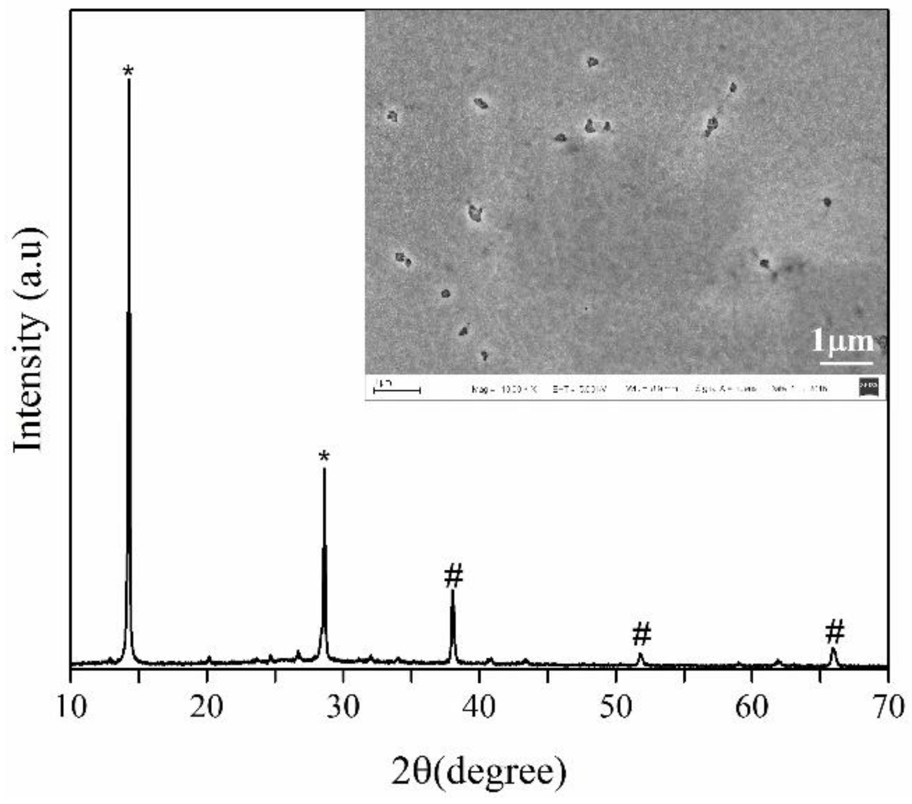
Given that the mechanism of the crystal formation is comprised of two steps of nucleation and crystal growth [13,30], the deposition of perovskite precursors was performed in two consecutive spinning speeds. Evaporation rate is lower at lower speeds, and therefore nucleation starts without substantial crystal growth. At a higher spinning speed, the evaporation rate increases, and the resulting supersaturation boosts the crystallization process. To further expedite the solvent extraction, toluene anti-solvent was dripped at the second spinning stage. Therefore, unless stated otherwise, the perovskite films in this work were prepared by one-step deposition of a mixture of precursor solutions, employing two consecutive spinning speeds. In the first stage of all cases, the film was spun at 1000 rpm for 15 s, whereas the speed of the second stage was either 4000 or 5000 rpm, for 40 s. Based on several optimization steps, we found that 60 μl of toluene is the suitable amount of the anti-solvent to prepare a pure and high coverage MA-based perovskite film with an area of 10 × 10 mm, spun at 5000 rpm (Figure 2). The film coverage and the perovskite conversion mainly determine the rate of the charge generation and transport within the cell [10,31]. Figure 2, however, shows some manufacturing defects in the film, which affects the device performance.
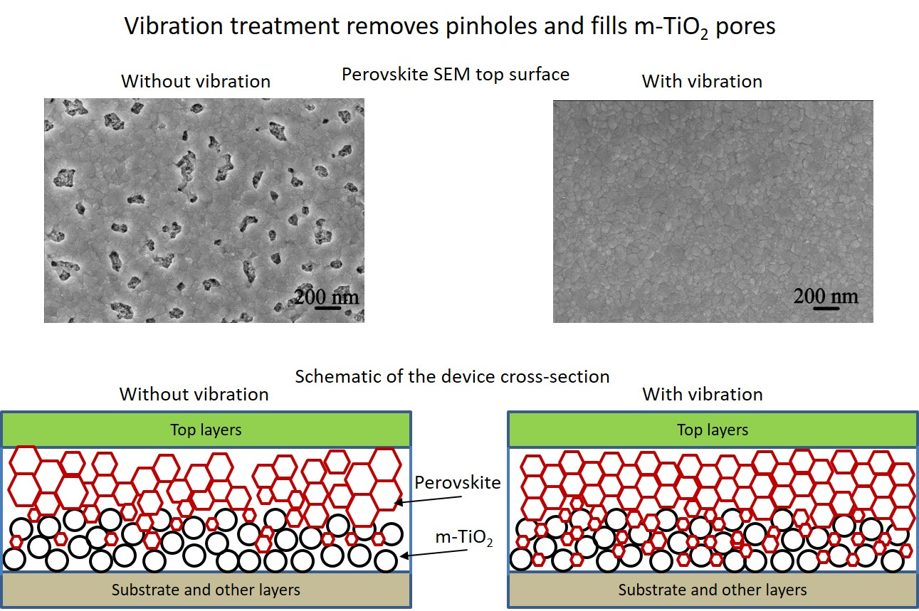
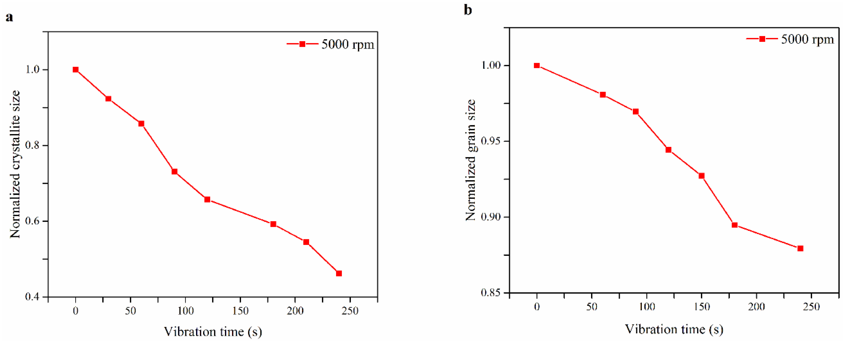
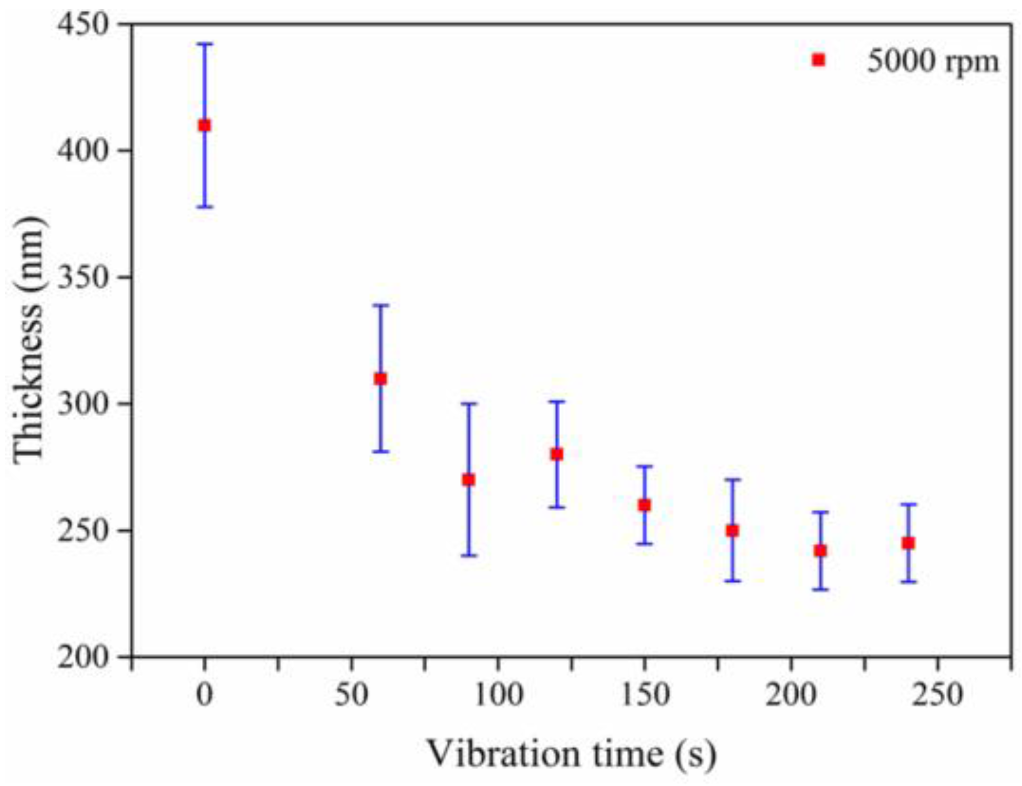
In the next step, to further control the mechanism of the crystal growth, we performed the SVPT on the as-spun wet perovskite films deposited atop the m-TiO2 layer for certain time durations. The XRD patterns and SEM images were employed to assess the perovskite inner crystallite and surface grain sizes, respectively. The x-ray incident angle was set at 14.2° and the constant in the Scherrer equation was set to 0.9. The top view SEM images show the size and shape of the surface grains, whereas the values obtained using the XRD-based Scherrer equation [32,33] are more representative of the perovskite grains in the three-dimensional (3D) lattice. It is also noted that the Scherrer equation is accurate for crystals smaller than 100 nm [34], and large surface grains cannot be estimated using the XRD patterns. The XRD and SEM grain sizes are shown in Figure 3a,b, respectively. The sample prepared without the SVPT has XRD and SEM grain sizes of 65 and 130 nm, respectively. As the measurements show, the surface grains observed under the SEM are larger than those within the film detected and measured by the XRD. Nevertheless, the results based on the XRD and SEM affirm that the size of the perovskite grains almost linearly decrease with the duration of the SVPT. Figure 3a shows about 40% decrease in the grain size, if the SVPT is applied for 120 s. Imposed vibration results in an increase in the evaporation rate [23], an increase in the nucleation rate, and a decrease in the activation energy of crystallization [35], which seem to result in a decrease in the grain size. However, the main reason for a decrease in the perovskite grain size in the perovskite/m-TiO2 system is due to an enhanced infiltration of the pores of the mesoporous layer by the perovskite precursors. This improved perovskite penetration hypothesis is supported by the thickness data of the MAPbI3 perovskite layers deposited atop the m-TiO2 layer, as illustrated in Figure 4, which shows a decrease in the perovskite thickness with the vibration time.
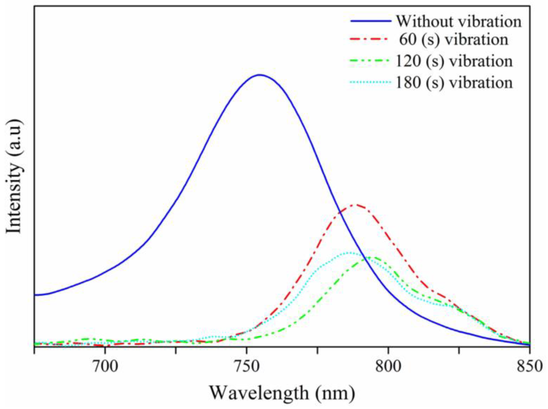
The enhanced infiltration of the m-TiO2 pores by the perovskite precursors leads to an increase in the contact surface between the perovskite and the TiO2 nanoparticles, within the m-TiO2 layer. This brings about improved pathways for the charge transport from the perovskite crystals to the ETL, although a decreased perovskite grain size, as a result of the SVPT, may potentially create additional charge trap sites at the boundaries, which may cause a reduced charge injection rate. To investigate the latter, the corresponding steady state PL spectra of the perovskite films deposited atop the m-TiO2 layer, without and with the SVPT, are shown in Figure 5. The emission peak appearing between 700 and 850 nm indicates the well-known 1.6 eV band gap of the MAPbI3 perovskite [7]. The PL intensity is stronger for the pristine sample. The reduced PL intensity in the SVPT samples is indicative of higher charge injection into the TiO2 layer [36], which implies that by applying the SVPT, the contact between the TiO2 ETL and the perovskite light absorber has improved. It is also speculated that a decrease in the film thickness (c.f. Figure 4), as a result of the imposed vibration, while the film intactness is maintained, contributes to the improvement of the charge transport from the perovskite layer to the ETL.
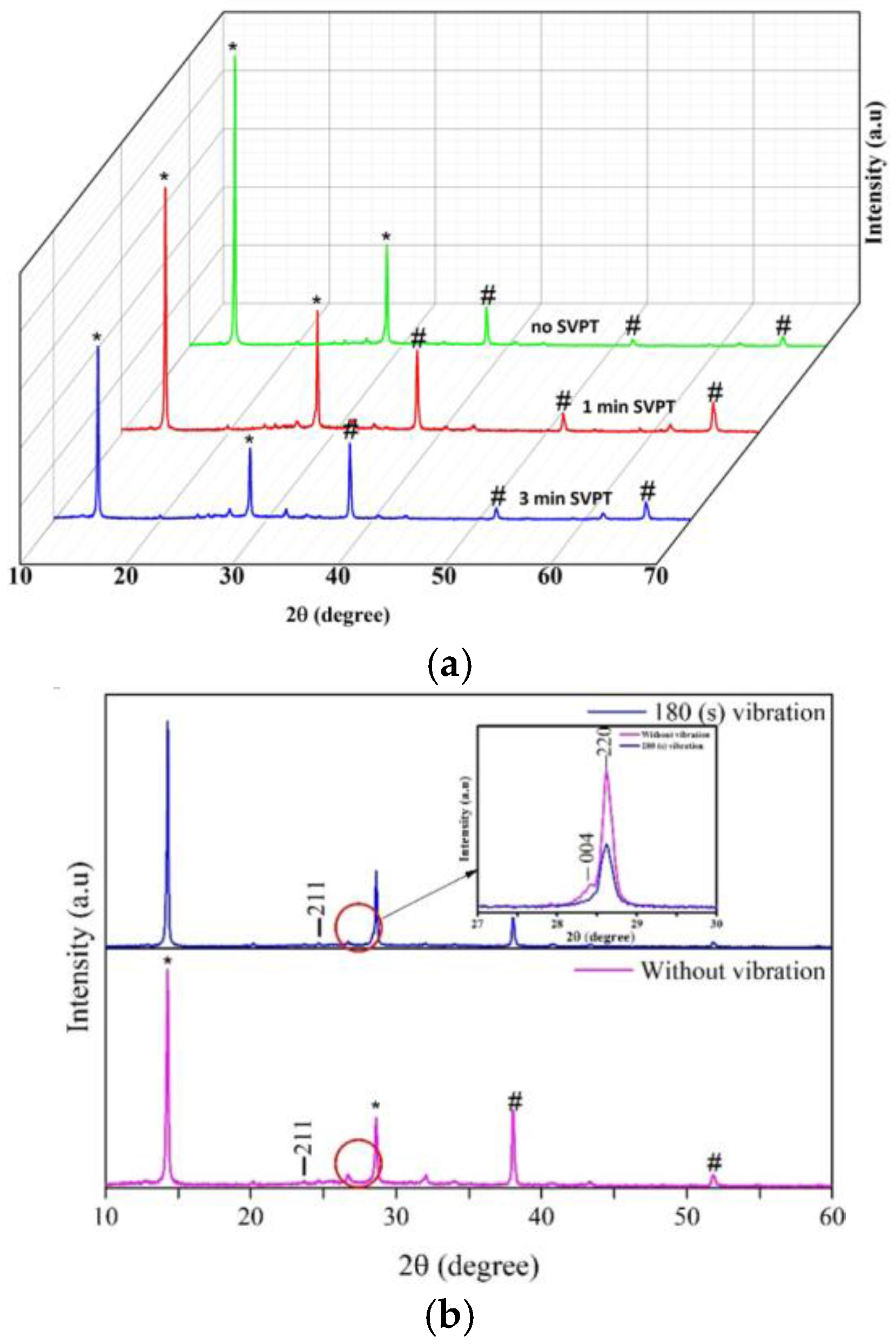
The PL peaks of Figure 5 exhibit a significant systematic red shift occurring due to the SVPT. The occurrence of the red shift may be attributed to a change in the perovskite crystal lattice parameters and/or the inclusion of defects or self-absorption in a thinner perovskite film, as caused by the vibrational excitations. It has been proposed that crystallites of the tetragonal phase of perovskite (as usually observed in PSCs) may co-exist with the orthorhombic phase, which form at room temperature [37]. It is also known that various phases form in different temperatures, where the temperature required for a structural phase transition increases with the thickness of the perovskite film [38]. Given that the imposed vibration affects the film thickness, and consequently, the phase transition temperature, one may speculate that a small amount of the orthorhombic phase may co-exist with the main tetragonal phase. To investigate this, the overall XRD patterns of the pristine and the SVPT MAPbI3 films were obtained (Figure 6a). The peaks of the tetragonal phase are clearly dominant. Therefore, the hypothesis for the formation of the orthorhombic phase may be ruled out. The detailed XRD of the pristine and the film subjected to the SVPT for 180 s are shown in Fig. 6b. It is observed that a minor peak exists at the (004) plane associated with 28.3° angle, which disappears when the film is subjected to the SVPT for 180 s, while the peak associated with the (211) plane still exists, which indicates that the crystal structure is still tetragonal. Merger of the peaks at 28.3° and 28.6° has been attributed to crystal distortion, and therefore, a change in the lattice parameters [39]. Thus, excitation of the perovskite by the vibration results in a slight lattice distortion and a change in the lattice parameters. A change in the peak position, intensity, and width has been observed in PbI2 crystals subjected to the SVPT, as well [35]. Additionally, the red shift may be due to an increase in the extrinsic defects, such as the fraction of the grain boundaries in the crystal lattice [40], which indeed increases with the application of vibration, through a decrease in the crystallite size, a conclusion that is backed by the findings of this work, e.g., Figure 3.
The effect of the crystal size on the device performance is controversial. Some studies are in favor of smaller crystal sizes, whereas some other recommend otherwise [41]. Nie et al. have reported that larger grain sizes are beneficial [42], whereas here we observed that while the application of the SVPT results in a decrease in the grain size, the charge transport from the perovskite layer to the ETL layer is improved (PL spectra). Therefore, it may be deduced that the improved coverage and the contact surface between the perovskite layer and the TiO2 nanoparticles, as caused by the SVPT, is responsible for the improved charge transport. Figure 7 illustrates the SEM images of the pristine and SVPT perovskite layers spun atop the m-TiO2 layer at 5000 rpm. It is observed that the morphology of the perovskite film is improved with an increase in the duration of the SVPT, and the best morphology (Figure 7) and PL spectra (Figure 5) are obtained at the SVPT time duration of 180 s. The SVPT imparts energy to the wet film, and therefore creates micromixing [25] and in-situ heating, which tends to homogenize the perovskite solution, leading to the formation of a uniform and high coverage film.
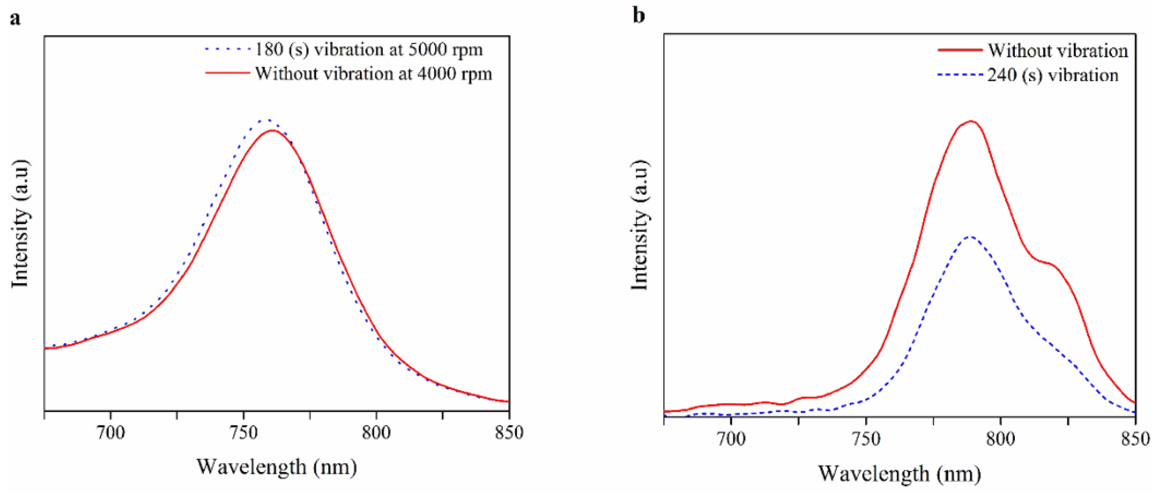
Since the perovskite film thickness and crystal size vary with the spinning speed, in another series of experiments, the spinning speed was decreased from 5000 to 4000 rpm, to further investigate how the SVPT affects thicker films. The PL spectra of a perovskite film spun at 4000 rpm is compared with that of the best sample of the previous cases, i.e., the film spun at 5000 rpm, using 180 s of the SVPT (Figure 8a). Figure 8a shows that the lower spin speed of 4000 rpm results in a better charge extraction. Hence, the effect of the SVPT was further explored on the perovskite films that were spun at 4000 rpm (Figure 8b). A much weaker PL intensity is observed in the sample subjected to the SVPT for 240 s, which is an indicative of a better charge transport. To study the surface morphology, Figure 9 shows the SEM images of pristine and the SVPT MAPbI3 samples spun at 4000 rpm. It is observed that the long-duration vibration of 240 s results in a decrease in the grain size and emergence of pinholes. Despite the appearance of the pinholes, this sample shows a superior charge transfer as compared with the pristine sample (Figure 8b). While vibration has a similar positive effect on both cases, comparison of the SEM images of the perovskite films spun at 4000 rpm (Figure 9) and 5000 rpm (Figure 7) reveals that the film spun at 5000 rpm and subjected to 180 s of the SVPT shows a more desirable uniformity and coverage, and therefore 5000 rpm is selected as the optimum case for device fabrication.
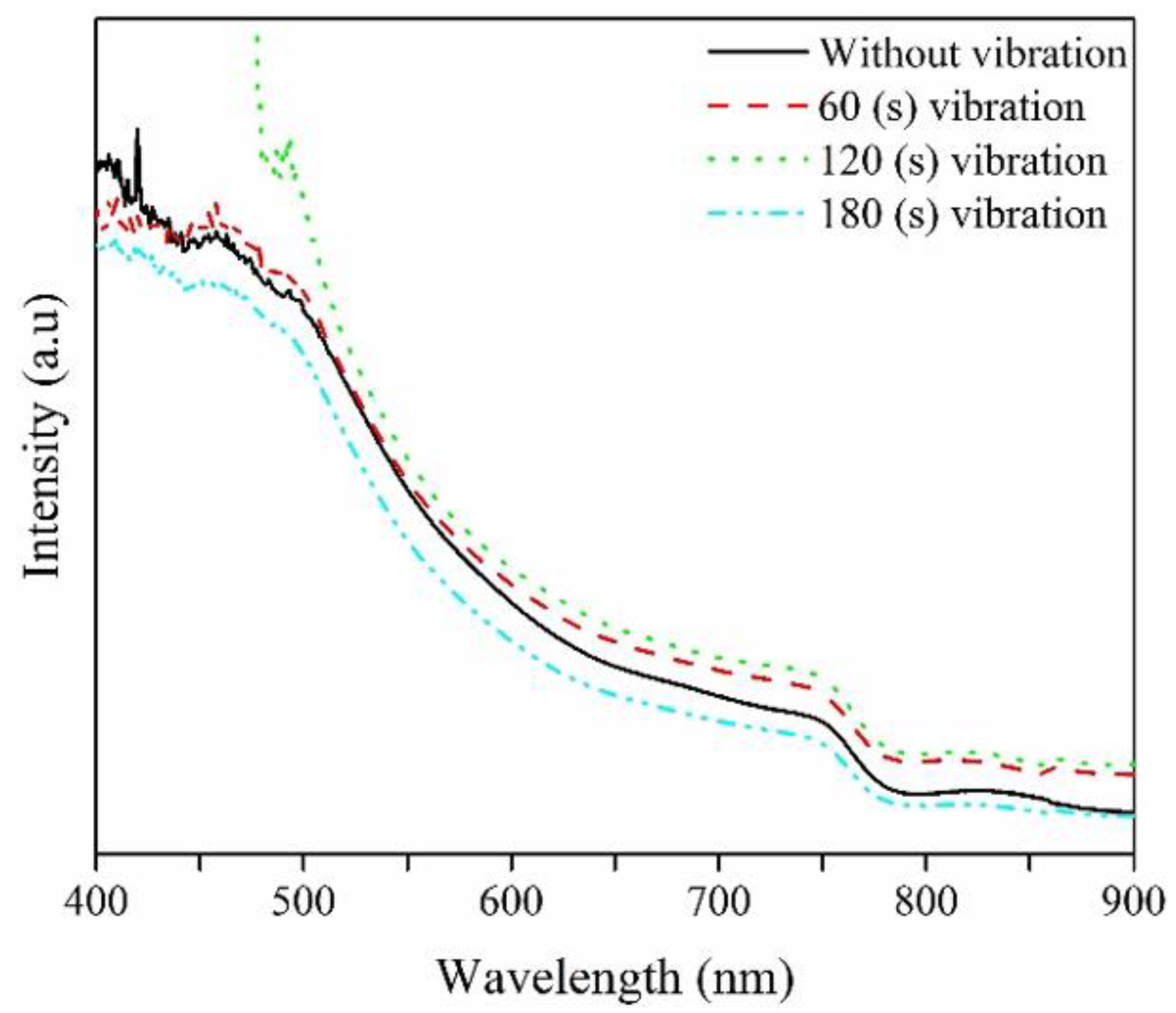
The absorbance spectra of the pristine and the SVPT MAPbI3 films spun at 5000 rpm are shown in Figure 10. Absorbance is a measure of the capability of the film to absorb the photon energy to overcome the band gap. Some studies indicate that a larger perovskite crystal size (~1 µm) favors the light absorbance [43,44]. Also, a thicker and highly covered and defect-free film favor the absorbance. Since in this study, the imposed vibration affects the crystal size, film thickness, and coverage, the sole effect of the vibration or crystal size on the absorbance cannot be deduced. The perovskite layer vibrated for 180 s has the lowest absorbance. Figure 3 shows that this sample has one of the smallest crystal sizes, and Figure 4 shows that the thickness of this film is almost half of that of the pristine film. Therefore, the reduced absorbance may be due to both a decreased crystal size and also a lower film thickness. It is noted that although the film that was subjected to the SVPT for 180 s has the lowest absorbance, it is the most intact, defect-free, and impurity-free film, with the best charge transfer capability.
It was previously observed that the PL spectra undergo a red shift as a result of the vibration (c.f. Figure 5), due to some changes in the lattice structure of the film. On the other hand, Figure 10 shows that there is no shift in the position of the sudden drop in the absorbance intensity (~780 nm), as a result of the vibration, which may be an indicative of insensitivity of the band gap to the vibration.
Table 1 summarizes the effect of the vibration time on major characteristics of the perovskite films spun at two speeds. It is corroborated that as the vibration time increases, the PL intensity decreases (charge transfer between the perovskite and the ETL is improved), the film thickness decreases (perovskite fills the gaps of the m-TiO2 layer), and the full width at half maximum (FWHM) in the XRD peaks increases (grain size decreases). Thus, one may conclude that the SVPT improves all of the characteristics of the MAPbI3 films, except for the absorbance.
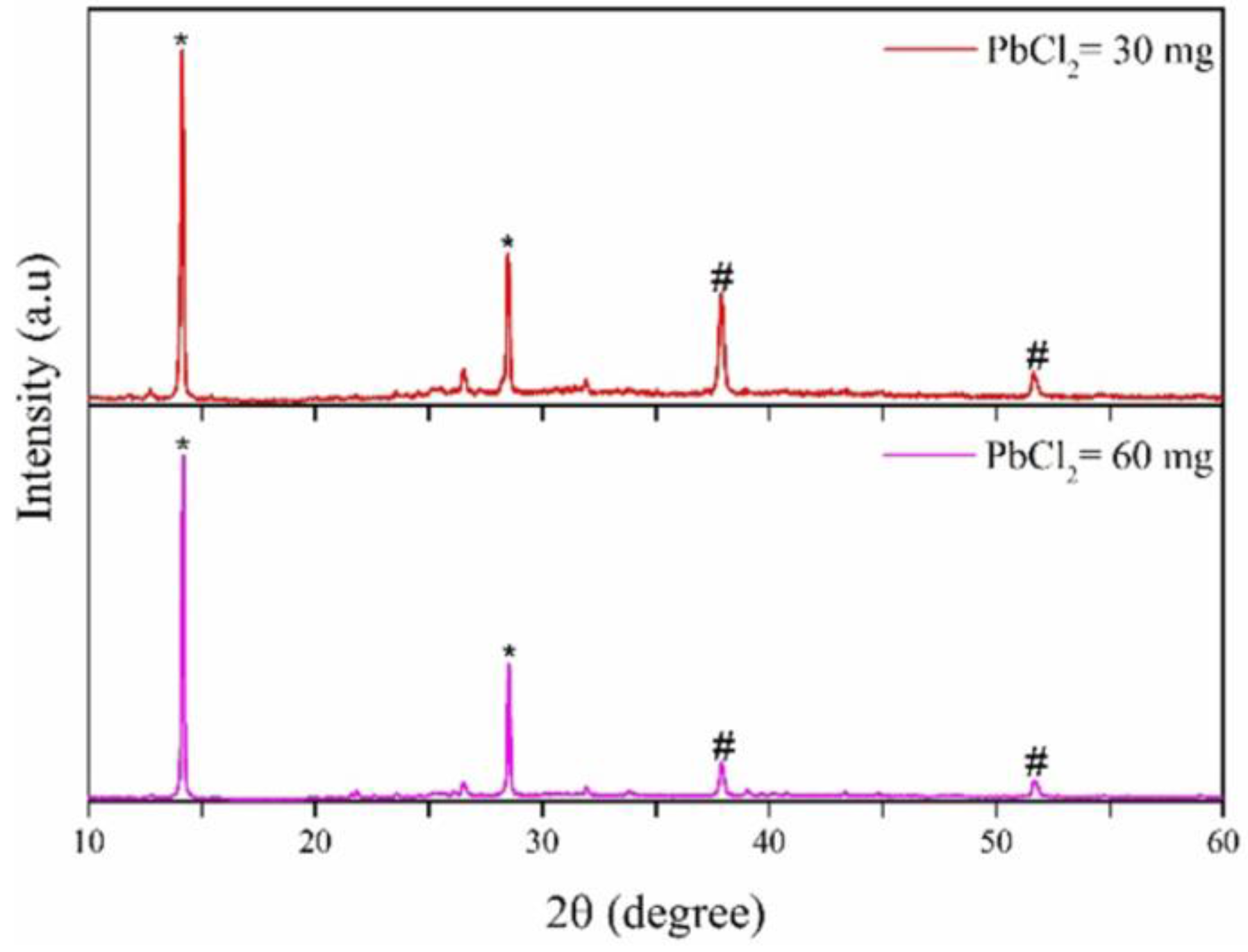
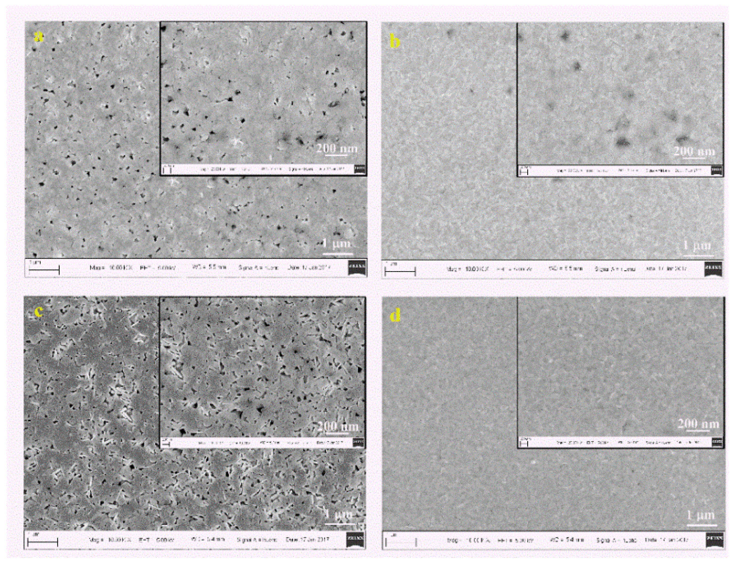
The previous experiments were performed on MAPbI3 perovskite. In an attempt to generalize the findings, selected experiments were performed on mixed halide perovskite (MAPbI3-xClx) films, spun at 5000 rpm. The XRD patterns of the MAPbI3-xClx films are shown in Figure 11, substantiating a complete conversion of the precursors to perovskite. Comparison of the peaks of the MAPbI3 with those of the MAPbI3-xClx reveals that the position of the peak of the (110) plane for MAPbI3 is at 14.12°, while it changes to 14.25° for the sample with 30 mg of PbCl2. The other peaks remain at the same positons. Therefore, the addition of Cl slightly changes the perovskite lattice parameters. Figure 12 shows the SEM images of the MAPbI3-xClx films, where the effect of the perovskite composition and the vibration treatment for 180 s is demonstrated. Again, the SVPT improves the film quality, significantly. The chlorine-rich film subjected to the SVPT for 180 s has a pinhole-free morphology. Comparison of Figure 7 and Figure 12 reveals that both single and mixed halide perovskite films spun at 5000 rpm, followed by the SVPT for 180 s exhibit a defect-free morphology. This approach introduces the SVPT as a low-cost universal approach for the fabrication of defect-free perovskite films on the m-TiO2 layer, which could also be employed in spray coating, blade coating, and other casting methods.
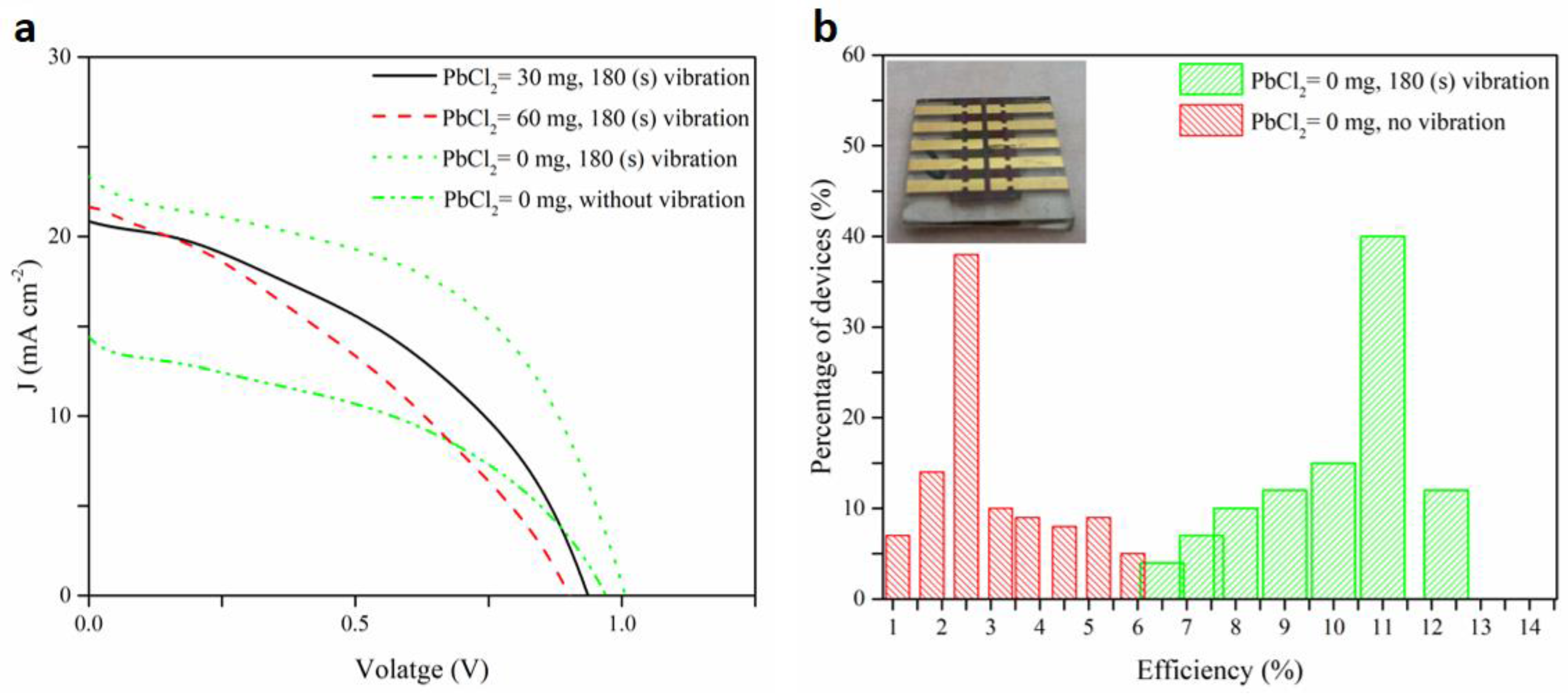
Overall, when considering the foregoing results and discussion, one may conclude that the single and mixed halide perovskite films spun at 5000 rpm for 40 s and followed by the SVPT for 180 s exhibit the best performance. As a proof of concept, single and mixed halide perovskite devices were fabricated, without additional treatments on other layers. The devices have the basic structure of glass/TCO/c-TiO2/m-TiO2/perovskite/HTL/Au. Similar devices fabricated using the one-step method without additional interface engineering typically have shown the PCE of about 6–9% [45]. More recent studies have achieved higher PCE through the optimization of the m-TiO2 and other layers [40]. The photovoltaic parameters and the JV curves of the champion devices are shown in Table 2 and Figure 13a. The results show that the single halide devices (MAPbI3) have a higher performance, as observed by others, as well [46]. The MAPbI3 device subjected to the SVPT shows a PCE of 12.51%, significantly higher than that of the pristine device (6%). The short circuit current density (Jsc) and fill factor (FF) of the SVPT devices are significantly improved with respect to the control devices, which is attributed to the effective infiltration of the pores of the m-TiO2 layer by the perovskite solution, as a result of the imposed ultrasonic vibration. Table 2 also shows the estimated shunt and series resistances of the champion devices. A low series resistance and high shunt resistance is desirable for the optimum device performance. The data show that the SVPT significantly increases the shunt resistance. However, the shunt resistances are still low [47]. The low shunt resistance and the low FF are due to manufacturing defects of all the layers. Optimization of other layers, such as the HTL, and employing compositional and interface engineering [48] would further increase the photovoltaic parameters, albeit at the expense of additional steps and costs. Finally, Figure 13b shows the histogram of 50 MAPbI3 devices treated with the SVPT for 180 s, as well as the histogram of the control devices. It is observed that the PCE of over 50% of the SVPT devices is greater than 11%, which indicates that the SVPT devices are more repeatable and reproducible than the pristine devices.
4. Conclusions
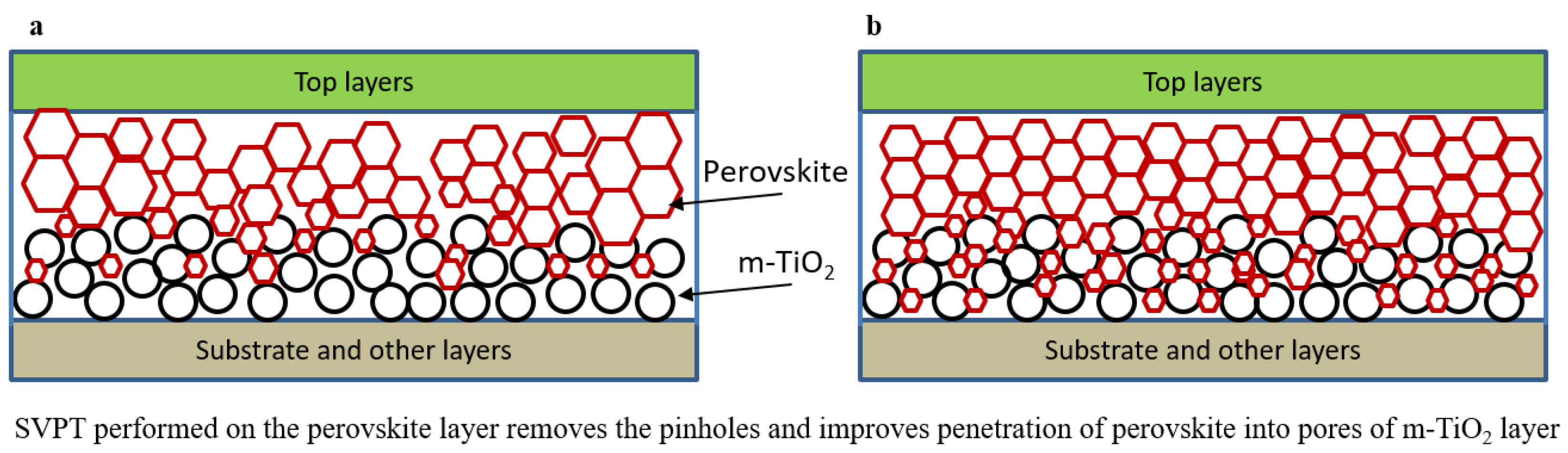
In this work, the effects of the imposed ultrasonic vibration on the various characteristics of the perovskite thin films and the device performance were studied. In summary, Figure 14 schematically shows that the application of the ultrasonic SVPT results in smaller crystal size, better infiltration of the pores of the m-TiO2 film by the perovskite solution (substantiated by a decrease in the film thickness as a result of the SVPT), better contact between the perovskite and the m-TiO2 nanoparticles, and the elimination of pinholes, all of which are supported by the results of this work. It was also shown that the charge injection and transport from the perovskite film to the ETL increases as the vibration time increases (from 0 to about 180 s).
The aforementioned results lead us to conclude that with the imposed vibration, the contact between the perovskite crystals and the m-TiO2 layer is improved, even though the crystal size decreases. Thus, the effective contact between perovskite and the ETL was found to be more important on the device performance than the crystal size. In view of these results, the application of the SVPT could result in further improvement in the performance of the state-of-the-art PSCs, in terms of the efficiency, reducing the fabrication costs, and improving the repeatability and reproducibility. Finally, it is noted that the SVPT is compatible with the scalable methods, such as spray and blade coating, and can be used to develop annealing-free PSCs [49], although obtaining uniform large-area thin films with any method is still challenging.
Acknowledgments
Financial support from the Shanghai Municipal Education Commission via the Oriental Scholar fund and the funding form the National Natural Science Foundation of China (NSFC) is acknowledged. Authors wish to thank Sanjib Das, Department of Materials Science and Engineering, Northwestern University, and Qianli Chen, University of Michigan-Shanghai Jiao Tong University Joint Institute, for fruitful discussions.
Author Contributions
All authors conceived the main idea of the paper. Mohammad-Reza Ahmadian-Yazdi and Mehran Habibi designed the experiments; Mohammad-Reza Ahmadian-Yazdi performed most of the experiments and analyzed the data; Mehran Habibi performed some of the experiments. Mohammad-Reza Ahmadian-Yazdi and Morteza Eslamian wrote the paper and discussed the results.
Conflicts of Interest
The authors declare no conflict of interest.
References
- National Renewable Energy Laboratory. Efficiency Chart. Available online: https://www.nrel.gov/pv/assets/images/efficiency-chart.png (accessed on 8 February 2018).
- Saliba, M.; Matsui, T.; Domanski, K.; Seo, J.-Y.; Ummadisingu, A.; Zakeeruddin, S.M.; Correa-Baena, J.-P.; Tress, W.R.; Abate, A.; Hagfeldt, A.; et al. Incorporation of rubidium cations into perovskite solar cells improves photovoltaic performance. Science 2016, 354, 206–209. [Google Scholar] [CrossRef] [PubMed]
- Saliba, M.; Matsui, T.; Seo, J.-Y.; Domanski, K.; Correa-Baena, J.-P.; Nazeeruddin, M.K.; Zakeeruddin, S.M.; Tress, W.; Abate, A.; Hagfeldt, A.; et al. Cesium-containing triple cation perovskite solar cells: Improved stability, reproducibility and high efficiency. Energy Environ. Sci. 2016, 9, 1989–1997. [Google Scholar] [CrossRef] [PubMed]
- Habibi, M.; Zabihi, F.; Ahmadian-Yazdi, M.R.; Eslamian, M. Progress in emerging solution-processed thin film solar cells – part II: Perovskite solar cells. Renew. Sustain. Energy Rev. 2016, 62, 1012–1031. [Google Scholar] [CrossRef]
- Pellet, N.; Gao, P.; Gregori, G.; Yang, T.-Y.; Nazeeruddin, M.K.; Maier, J.; Grätzel, M. Mixed-organic-cation perovskite photovoltaics for enhanced solar-light harvesting. Angew. Chem. Int. Ed. 2014, 53, 3151–3157. [Google Scholar] [CrossRef] [PubMed]
- Sun, Y.; Peng, J.; Chen, Y.; Yao, Y.; Liang, Z. Triple-cation mixed-halide perovskites: Towards efficient, annealing-free and air-stable solar cells enabled by Pb(SCN)2 additive. Sci. Rep. 2017, 7, 46193. [Google Scholar] [CrossRef] [PubMed]
- Jung, H.S.; Park, N.-G. Perovskite solar cells: From materials to devices. Small 2015, 11, 10–25. [Google Scholar] [CrossRef] [PubMed]
- Nejand, B.A.; Gharibzadeh, S.; Ahmadi, V.; Shahverdi, H.R. Novel solvent-free perovskite deposition in fabrication of normal and inverted architectures of perovskite solar cells. Sci. Rep. 2016, 6, 33649. [Google Scholar] [CrossRef] [PubMed]
- Wang, Q.; Chueh, C.-C.; Eslamian, M.; Jen, A.K.Y. Modulation of PEDOT: PSS pH for efficient inverted perovskite solar cells with reduced potential loss and enhanced stability. ACS Appl. Mater. Interfaces 2016, 8, 32068–32076. [Google Scholar] [CrossRef] [PubMed]
- Xu, W.; McLeod, J.A.; Yang, Y.; Wang, Y.; Wu, Z.; Bai, S.; Yuan, Z.; Song, T.; Wang, Y.; Si, J.; et al. Iodomethane-mediated organometal halide perovskite with record photoluminescence lifetime. ACS Appl. Mater. Interfaces 2016, 8, 23181–23189. [Google Scholar] [CrossRef] [PubMed]
- Bai, S.; Jin, Y.; Gao, F. Organometal halide perovskites for photovoltaic applications. In Advanced Functional Materials; Tiwari, A., Uzun, L., Eds.; John Wiley and Sons, Inc.: Hoboken, NJ, USA, 2015; pp. 535–566. [Google Scholar] [CrossRef]
- Eperon, G.E.; Stranks, S.D.; Menelaou, C.; Johnston, M.B.; Herz, L.M.; Snaith, H.J. Formamidinium lead trihalide: A broadly tunable perovskite for efficient planar heterojunction solar cells. Energy Environ. Sci. 2014, 7, 982–988. [Google Scholar] [CrossRef]
- Heo, J.H.; Song, D.H.; Im, S.H. Planar CH3NH3PbBr3 hybrid solar cells with 10.4% power conversion efficiency, fabricated by controlled crystallization in the spin-coating process. Adv. Mater. 2014, 26, 8179–8183. [Google Scholar] [CrossRef] [PubMed]
- Docampo, P.; Hanusch, F.C.; Stranks, S.D.; Döblinger, M.; Feckl, J.M.; Ehrensperger, M.; Minar, N.K.; Johnston, M.B.; Snaith, H.J.; Bein, T. Solution deposition-conversion for planar heterojunction mixed halide perovskite solar cells. Adv. Energy Mater. 2014, 4. [Google Scholar] [CrossRef]
- Zuo, C.; Ding, L. An 80.11% FF record achieved for perovskite solar cells by using the NH4Cl additive. Nanoscale 2014, 6, 9935–9938. [Google Scholar] [CrossRef] [PubMed]
- Colella, S.; Mosconi, E.; Fedeli, P.; Listorti, A.; Gazza, F.; Orlandi, F.; Ferro, P.; Besagni, T.; Rizzo, A.; Calestani, G.; et al. MAPbI3−xClx mixed halide perovskite for hybrid solar cells: The role of chloride as dopant on the transport and structural properties. Chem. Mater. 2013, 25, 4613–4618. [Google Scholar] [CrossRef]
- Liang, P.-W.; Liao, C.-Y.; Chueh, C.-C.; Zuo, F.; Williams, S.T.; Xin, X.-K.; Lin, J.; Jen Alex, K.-Y. Additive enhanced crystallization of solution-processed perovskite for highly efficient planar-heterojunction solar cells. Adv. Mater. 2014, 26, 3748–3754. [Google Scholar] [CrossRef] [PubMed]
- Jeon, N.J.; Noh, J.H.; Kim, Y.C.; Yang, W.S.; Ryu, S.; II Seok, S. Solvent engineering for high-performance inorganic-organic hybrid perovskite solar cells. Nat. Mater. 2014, 13, 897. [Google Scholar] [CrossRef] [PubMed]
- Xia, B.; Wu, Z.; Dong, H.; Xi, J.; Wu, W.; Lei, T.; Xi, K.; Yuan, F.; Jiao, B.; Xiao, L.; et al. Formation of ultrasmooth perovskite films toward highly efficient inverted planar heterojunction solar cells by micro-flowing anti-solvent deposition in air. J. Mater. Chem. A 2016, 4, 6295–6303. [Google Scholar] [CrossRef]
- Xie, Y.; Zabihi, F.; Eslamian, M. Fabrication of highly reproducible polymer solar cells using ultrasonic substrate vibration posttreatment. J. Photonics Energy 2016, 6, 045502. [Google Scholar] [CrossRef]
- Zabihi, F.; Chen, Q.; Xie, Y.; Eslamian, M. Fabrication of efficient graphene-doped polymer/fullerene bilayer organic solar cells in air using spin coating followed by ultrasonic vibration post treatment. Superlattices Microstruct. 2016, 100, 1177–1192. [Google Scholar] [CrossRef]
- Zabihi, F.; Ahmadian-Yazdi, M.-R.; Eslamian, M. Fundamental study on the fabrication of inverted planar perovskite solar cells using two-step sequential substrate vibration-assisted spray coating (2S-SVASC). Nanoscale Res. Lett. 2016, 11, 71. [Google Scholar] [CrossRef] [PubMed]
- Rahimzadeh, A.; Eslamian, M. On evaporation of thin liquid films subjected to ultrasonic substrate vibration. Int. Commun. Heat Mass Transf. 2017, 83, 15–22. [Google Scholar] [CrossRef]
- Rahimzadeh, A.; Eslamian, M. Stability of thin liquid films subjected to ultrasonic vibration and characteristics of the resulting thin solid films. Chem. Eng. Sci. 2017, 158, 587–598. [Google Scholar] [CrossRef]
- Eslamian, M. Excitation by acoustic vibration as an effective tool for improving the characteristics of the solution-processed coatings and thin films. Prog. Org. Coat. 2017, 113, 60–73. [Google Scholar] [CrossRef]
- Habibi, M.; Rahimzadeh, A.; Eslamian, M. On dewetting of thin films due to crystallization (crystallization dewetting). Eur. Phys. J. E 2016, 39, 30. [Google Scholar] [CrossRef] [PubMed]
- Carnie, M.J.; Charbonneau, C.; Davies, M.L.; Troughton, J.; Watson, T.M.; Wojciechowski, K.; Snaith, H.; Worsley, D.A. A one-step low temperature processing route for organolead halide perovskite solar cells. Chem. Commun. 2013, 49, 7893–7895. [Google Scholar] [CrossRef] [PubMed]
- Pei, Y.; Zou, X.; Qi, X.; Teng, G.; Li, Q.; Guo, D.; Zeng, S. Effect of perovskite film preparation on performance of solar cells. J. Chem. 2016, 2016, 10. [Google Scholar] [CrossRef]
- Xu, Q.-Y.; Yuan, D.-X.; Mu, H.-R.; Igbari, F.; Bao, Q.; Liao, L.-S. Efficiency enhancement of perovskite solar cells by pumping away the solvent of precursor film before annealing. Nanoscale Res. Lett. 2016, 11, 248. [Google Scholar] [CrossRef] [PubMed]
- Ahmadian-Yazdi, M.R.; Zabihi, F.; Habibi, M.; Eslamian, M. Effects of process parameters on the characteristics of mixed-halide perovskite solar cells fabricated by one-step and two-step sequential coating. Nanoscale Res. Lett. 2016, 11, 408. [Google Scholar] [CrossRef] [PubMed]
- Yan, J.; Zhang, B.; Chen, Y.; Zhang, A.; Ke, X. Improving the photoluminescence properties of perovskite CH3NH3PbBr3−xClx films by modulating organic cation and chlorine concentrations. ACS Appl. Mater. Interfaces 2016, 8, 12756–12763. [Google Scholar] [CrossRef] [PubMed]
- Zhang, W.; Saliba, M.; Moore, D.T.; Pathak, S.K.; Hörantner, M.T.; Stergiopoulos, T.; Stranks, S.D.; Eperon, G.E.; Alexander-Webber, J.A.; Abate, A.; et al. Ultrasmooth organic–inorganic perovskite thin-film formation and crystallization for efficient planar heterojunction solar cells. Nat. Commun. 2015, 6, 6142. [Google Scholar] [CrossRef] [PubMed] [Green Version]
- Patterson, A.L. The scherrer formula for x-ray particle size determination. Phys. Rev. 1939, 56, 978–982. [Google Scholar] [CrossRef]
- Zhou, Y.; Vasiliev, A.L.; Wu, W.; Yang, M.; Pang, S.; Zhu, K.; Padture, N.P. Crystal morphologies of organolead trihalide in mesoscopic/planar perovskite solar cells. J. Phys. Chem. Lett. 2015, 6, 2292–2297. [Google Scholar] [CrossRef] [PubMed]
- Zabihi, F.; Eslamian, M. Effect of the ultrasonic substrate vibration on nucleation and crystallization of PbI2 crystals and thin films. Crystals 2018, 8, 60. [Google Scholar] [CrossRef]
- Ko, H.-S.; Lee, J.-W.; Park, N.-G. 15.76% efficiency perovskite solar cells prepared under high relative humidity: Importance of PbI2 morphology in two-step deposition of CH3NH3PbI3. J. Mater. Chem. A 2015, 3, 8808–8815. [Google Scholar] [CrossRef]
- Wehrenfennig, C.; Liu, M.; Snaith, H.J.; Johnston, M.B.; Herz, L.M. Charge carrier recombination channels in the low-temperature phase of organic-inorganic lead halide perovskite thin films. APL Mater. 2014, 2, 081513. [Google Scholar] [CrossRef]
- Li, D.; Wang, G.; Cheng, H.-C.; Chen, C.-Y.; Wu, H.; Liu, Y.; Huang, Y.; Duan, X. Size-dependent phase transition in methylammonium lead iodide perovskite microplate crystals. Nat. Commun. 2016, 7, 11330. [Google Scholar] [CrossRef] [PubMed]
- Fu, F.; Kranz, L.; Yoon, S.; Löckinger, J.; Jäger, T.; Perrenoud, J.; Feurer, T.; Gretener, C.; Buecheler, S.; Tiwari, A.N. Controlled growth of PbI2 nanoplates for rapid preparation of CH3NH3PbI3 in planar perovskite solar cells. Phys. Status Solidi A 2015, 212, 2708–2717. [Google Scholar] [CrossRef]
- Kong, W.; Ye, Z.; Qi, Z.; Zhang, B.; Wang, M.; Rahimi-Iman, A.; Wu, H. Characterization of an abnormal photoluminescence behavior upon crystal-phase transition of perovskite CH3NH3PbI3. Phys. Chem. Chem. Phys. 2015, 17, 16405–16411. [Google Scholar] [CrossRef] [PubMed]
- Kim, H.-S.; Park, N.-G. Parameters affecting I–V hysteresis of CH3NH3PbI3 perovskite solar cells: Effects of perovskite crystal size and mesoporous TiO2 layer. J. Phys. Chem. Lett. 2014, 5, 2927–2934. [Google Scholar] [CrossRef] [PubMed]
- Nie, W.; Tsai, H.; Asadpour, R.; Blancon, J.-C.; Neukirch, A.J.; Gupta, G.; Crochet, J.J.; Chhowalla, M.; Tretiak, S.; Alam, M.A.; et al. High-efficiency solution-processed perovskite solar cells with millimeter-scale grains. Science 2015, 347, 522–525. [Google Scholar] [CrossRef] [PubMed]
- Raga, S.R.; Jung, M.-C.; Lee, M.V.; Leyden, M.R.; Kato, Y.; Qi, Y. Influence of air annealing on high efficiency planar structure perovskite solar cells. Chem. Mater. 2015, 27, 1597–1603. [Google Scholar] [CrossRef]
- Xiao, Z.; Dong, Q.; Bi, C.; Shao, Y.; Yuan, Y.; Huang, J. Solvent annealing of perovskite-induced crystal growth for photovoltaic-device efficiency enhancement. Adv. Mater. 2014, 26, 6503–6509. [Google Scholar]
- Im, J.-H.; Kim, H.-S.; Park, N.-G. Morphology-photovoltaic property correlation in perovskite solar cells: One-step versus two-step deposition of CH3NH3PbI3. APL Mater. 2014, 2, 081510. [Google Scholar] [CrossRef]
- Shi, Y.; Xing, Y.; Li, Y.; Dong, Q.; Wang, K.; Du, Y.; Bai, X.; Wang, S.; Chen, Z.; Ma, T. CH3NH3PbI3 and CH3NH3PbI3−xClx in planar or mesoporous perovskite solar cells: Comprehensive insight into the dependence of performance on architecture. J. Phys. Chem. C 2015, 119, 15868–15873. [Google Scholar]
- Wu, C.G.; Chiang, C.H.; Tseng, Z.L.; Zazeeruddin, M.K.; Hagfeldt, A.; Gratzel, M. High efficiency stable inverted perovskite solar cells without current hysteresis. Energy Environ. Sci. 2015, 8, 2725–2733. [Google Scholar]
- Jiang, L.; Zheng, J.; Chen, W.; Huang, Y.; Hu, L.; Hayat, T.; Alsaedi, A.; Zhang, C.; Dai, S. High-performance perovskite solar cells with a weak covalent TiO2: Eu3+ mesoporous structure. ACS Appl. Energy Mater. 2017, 1, 93–102. [Google Scholar] [CrossRef]
- Ahmadian-Yazdi, M.-R.; Eslamian, M. Toward scale-up of perovskite solar cells: Annealing-free perovskite layer by low-cost ultrasonic substrate vibration of wet films. Mater. Today Commun. 2018, 14, 151–159. [Google Scholar] [CrossRef]
Figure 1.
Perovskite thin film deposition procedure, using the ultrasonic substrate vibration post treatment (SVPT) and annealing.
Figure 1.
Perovskite thin film deposition procedure, using the ultrasonic substrate vibration post treatment (SVPT) and annealing.

Figure 2.
XRD pattern and SEM image of the MAPbI3 perovskite films fabricated atop the m-TiO2 layer using the one-step deposition method at two consecutive spin speeds (spin speed in the second stage is 5000 rpm). The “*” denotes the perovskite peaks and “#” denotes the fluorine-doped tin oxide (FTO) peaks.

Figure 3.
Normalized (a) grain size obtained from the XRD patterns, and (b) the surface grain size obtained from the SEM images of the MAPbI3 perovskite films spun at 5000 rpm, for various time durations of the SVPT. The sizes were normalized with respect to the crystallite/grain sizes of the pristine samples, i.e., 65 nm in (a) and 130 nm in (b).

Figure 4.
Thickness of the MAPbI3 perovskite films deposited atop the m-TiO2 layers at various time durations of the SVPT.
Figure 4.
Thickness of the MAPbI3 perovskite films deposited atop the m-TiO2 layers at various time durations of the SVPT.

Figure 5.
Effect of the SVPT on the photoluminescence (PL) spectra of the MAPbI3 perovskite layers deposited atop the m-TiO2 layers. The spin speed in the second stage of the spinning is 5000 rpm.
Figure 5.
Effect of the SVPT on the photoluminescence (PL) spectra of the MAPbI3 perovskite layers deposited atop the m-TiO2 layers. The spin speed in the second stage of the spinning is 5000 rpm.

Figure 6.
(a) Effect of the SVPT time on XRD patterns of the MAPbI3 perovskite films. (b) Effect of the SVPT on crystal distortion. The “*”and “#” denote the perovskite and FTO peaks, respectively.
Figure 6.
(a) Effect of the SVPT time on XRD patterns of the MAPbI3 perovskite films. (b) Effect of the SVPT on crystal distortion. The “*”and “#” denote the perovskite and FTO peaks, respectively.

Figure 7.
SEM images of the MAPbI3 perovskite surface morphology, spun at 5000 rpm for (a) pristine sample, and the samples subjected to the SVPT for (b) 60 s, (c) 120 s, and (d) 180 s.
Figure 7.
SEM images of the MAPbI3 perovskite surface morphology, spun at 5000 rpm for (a) pristine sample, and the samples subjected to the SVPT for (b) 60 s, (c) 120 s, and (d) 180 s.
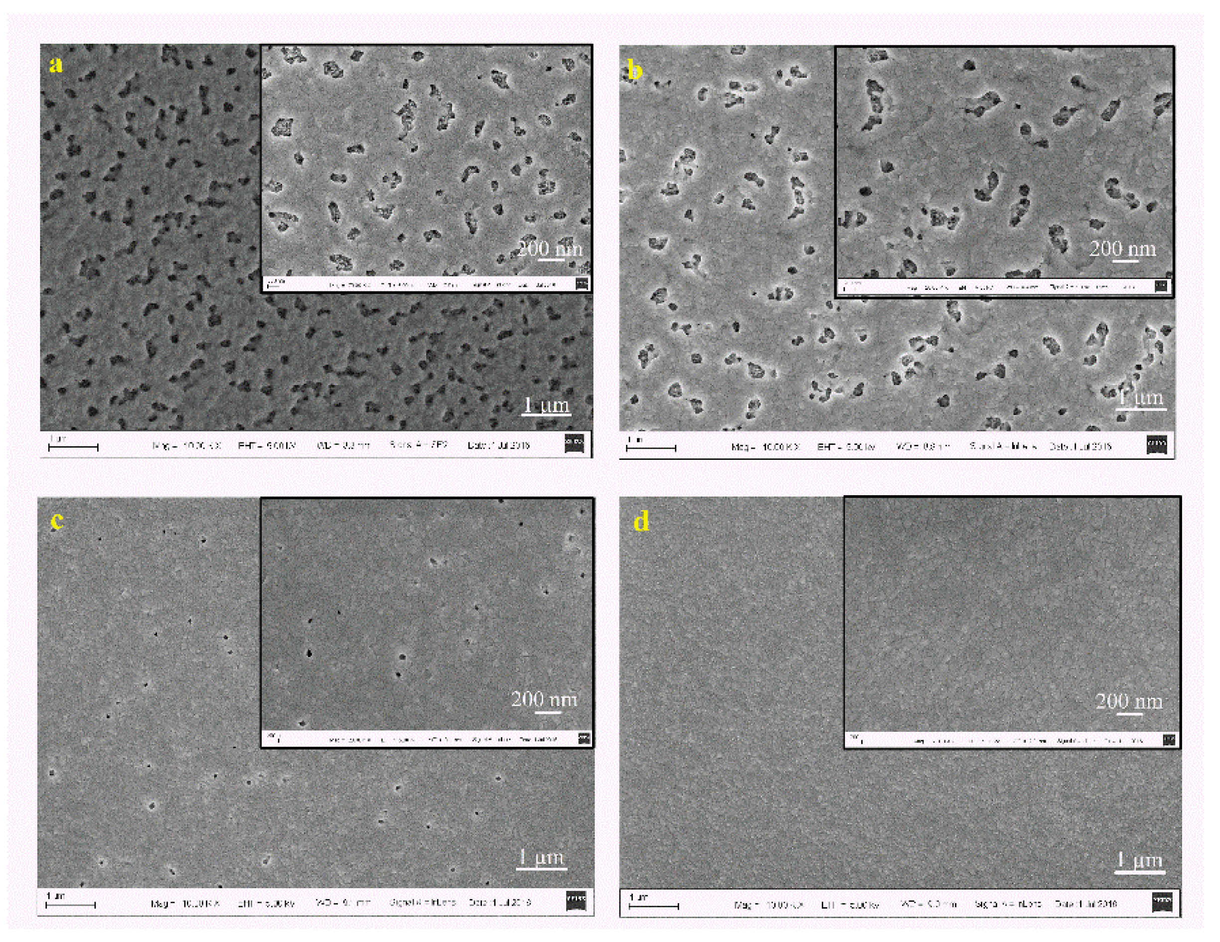
Figure 8.
Photoluminescence (PL) spectra of the MAPbI3 perovskite films deposited atop the m-TiO2 layers. (a) The best SVPT sample spun at 5000 rpm, and the pristine sample spun at 4000 rpm, and (b) samples spun at 4000 rpm with and without the SVPT.
Figure 8.
Photoluminescence (PL) spectra of the MAPbI3 perovskite films deposited atop the m-TiO2 layers. (a) The best SVPT sample spun at 5000 rpm, and the pristine sample spun at 4000 rpm, and (b) samples spun at 4000 rpm with and without the SVPT.

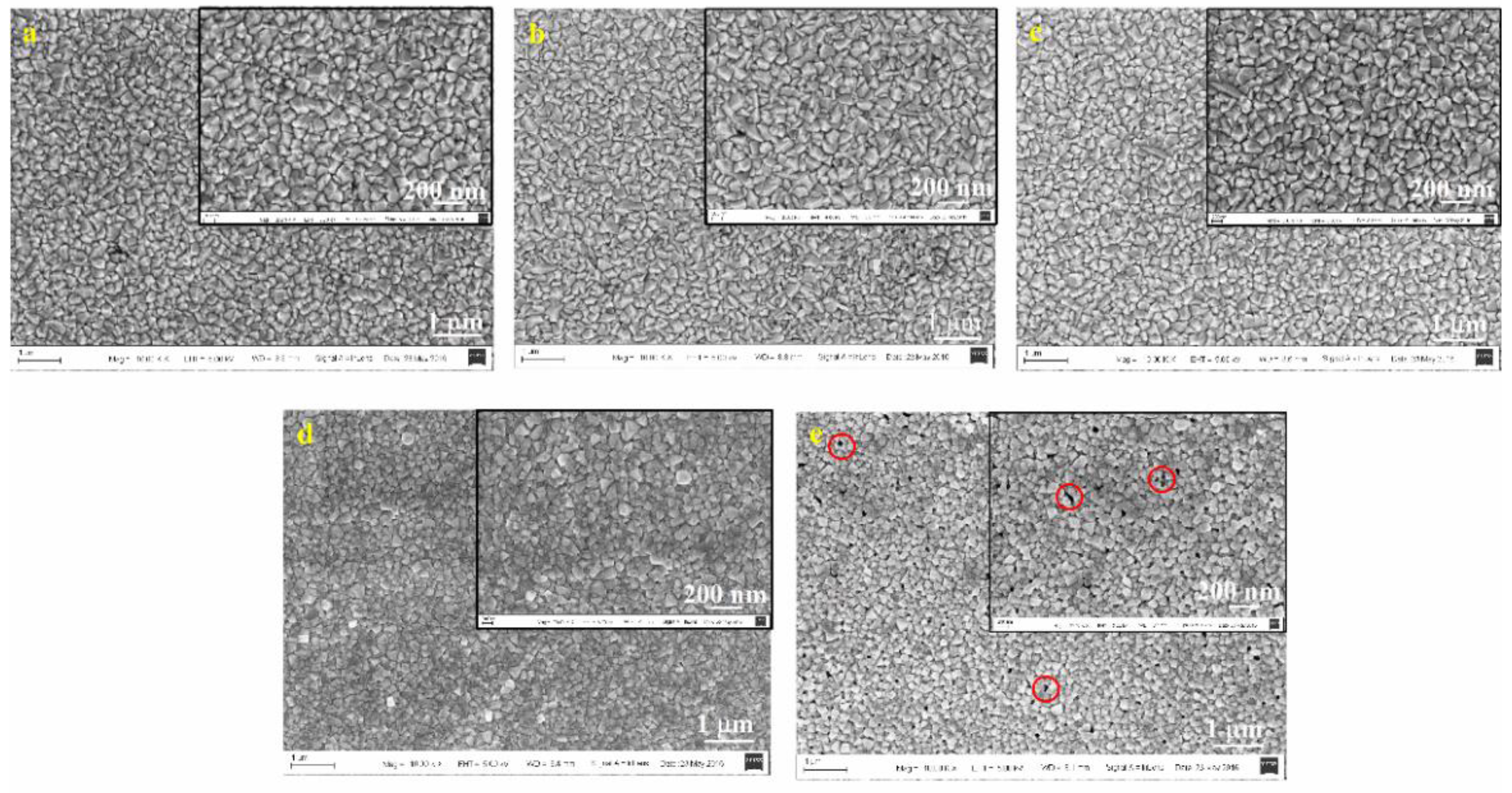
Figure 9.
SEM images of the MAPbI3 perovskite films spun at 4000 rpm. (a) Pristine sample, and the samples subjected to the SVPT for (b) 60 s, (c) 120 s, (d) 180 s, and (e) 240 s. In (e), the voids are circled.
Figure 9.
SEM images of the MAPbI3 perovskite films spun at 4000 rpm. (a) Pristine sample, and the samples subjected to the SVPT for (b) 60 s, (c) 120 s, (d) 180 s, and (e) 240 s. In (e), the voids are circled.

Figure 10.
Absorbance of the MAPbI3 perovskite films spun atop the m-TiO2 layers at 5000 rpm for several time durations of the SVPT.
Figure 10.
Absorbance of the MAPbI3 perovskite films spun atop the m-TiO2 layers at 5000 rpm for several time durations of the SVPT.

Figure 11.
XRD peaks of the mixed halide perovskites MAPbI3−xClx fabricated atop the m-TiO2 layers, at 5000 rpm. The “*” denotes the perovskite peaks and “#” denotes the FTO peaks.
Figure 11.
XRD peaks of the mixed halide perovskites MAPbI3−xClx fabricated atop the m-TiO2 layers, at 5000 rpm. The “*” denotes the perovskite peaks and “#” denotes the FTO peaks.

Figure 12.
SEM images of the mixed halide perovskite (MAPbI3−xClx) films spun at 5000 rpm. (a) Pristine sample (PbCl2 = 30 mg), (b) the sample subjected to the SVPT for 180 s (PbCl2 = 30 mg), (c) pristine sample (PbCl2 = 60 mg), and (d) the sample subjected to the SVPT for 180 s (PbCl2 = 60 mg).
Figure 12.
SEM images of the mixed halide perovskite (MAPbI3−xClx) films spun at 5000 rpm. (a) Pristine sample (PbCl2 = 30 mg), (b) the sample subjected to the SVPT for 180 s (PbCl2 = 30 mg), (c) pristine sample (PbCl2 = 60 mg), and (d) the sample subjected to the SVPT for 180 s (PbCl2 = 60 mg).

Figure 13.
(a) JV curves of the MAPbI3 and MAPbI3−xClx PSCs spun at 5000 rpm with and without the SVPT. The significant positive effect of the SVPT is demonstrated. (b) Histograms of the PCE of 50 MAPbI3 devices, fabricated without and with 180 s of the SVPT.
Figure 13.
(a) JV curves of the MAPbI3 and MAPbI3−xClx PSCs spun at 5000 rpm with and without the SVPT. The significant positive effect of the SVPT is demonstrated. (b) Histograms of the PCE of 50 MAPbI3 devices, fabricated without and with 180 s of the SVPT.

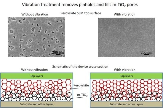
Figure 14.
Schematic diagram showing that the SVPT imposed on the wet perovskite layer improves the penetration of the perovskite solution into the pores of the m-TiO2 thin film. This results in the formation of smaller crystals and improvement in the contact between the perovskite and TiO2 nanoparticles. (a) Control device, and (b) the device subjected to the SVPT.


Table 1.
Effect of the vibration time for two spinning speeds on the characteristics of MAPbI3 layers.
Table 1.
Effect of the vibration time for two spinning speeds on the characteristics of MAPbI3 layers.
| Spin Speed (rpm) | Vibration Time (s) | PL Intensity (a.u) | Film Thickness (nm) | FWHM at 14° (degree) |
|---|---|---|---|---|
| 4000 | 0 | 0.44 | 450 | 0.12 |
| 4000 | 60 | 0.36 | 400 | 0.19 |
| 4000 | 120 | 0.34 | 400 | 0.20 |
| 4000 | 180 | 0.33 | 390 | 0.22 |
| 4000 | 240 | 0.27 | 388 | 0.26 |
| 5000 | 0 | 1.6 | 410 | 0.13 |
| 5000 | 60 | 0.73 | 310 | 0.14 |
| 5000 | 120 | 0.48 | 280 | 0.18 |
| 5000 | 180 | 0.46 | 245 | 0.20 |
Table 2.
Photovoltaic performance of the single and mixed halide Perovskite solar cells (PSCs). All of the devices were fabricated under identical conditions except for the ultrasonic substrate vibration post treatment (SVPT).
Table 2.
Photovoltaic performance of the single and mixed halide Perovskite solar cells (PSCs). All of the devices were fabricated under identical conditions except for the ultrasonic substrate vibration post treatment (SVPT).
| Sample | SVPT Time | RShunt (Ω·cm2) | RSeries (Ω·cm2) | Jsc (mA·cm−2) | Voc (V) | FF | PCE (%) |
|---|---|---|---|---|---|---|---|
| MAPbI3 | 180 s | 347 | 36.0 | 22.5 | 1.02 | 0.54 | 12.51 |
| MAPbI3 | Pristine | 74.0 | 41.0 | 14.5 | 0.98 | 0.42 | 6.00 |
| MAPbI3−xClx 1 | 180 s | 200 | 45.9 | 20.83 | 0.94 | 0.43 | 8.31 |
| MAPbI3−xClx 2 | 180 s | 127 | 21.6 | 21.77 | 0.89 | 0.36 | 6.97 |
1 PbCl2 = 30 mg; 2 PbCl2 = 60 mg.
© 2018 by the authors. Licensee MDPI, Basel, Switzerland. This article is an open access article distributed under the terms and conditions of the Creative Commons Attribution (CC BY) license (http://creativecommons.org/licenses/by/4.0/).
Share and Cite
MDPI and ACS Style
Ahmadian-Yazdi, M.-R.; Habibi, M.; Eslamian, M. Excitation of Wet Perovskite Films by Ultrasonic Vibration Improves the Device Performance. Appl. Sci. 2018, 8, 308. https://doi.org/10.3390/app8020308
AMA Style
Ahmadian-Yazdi M-R, Habibi M, Eslamian M. Excitation of Wet Perovskite Films by Ultrasonic Vibration Improves the Device Performance. Applied Sciences. 2018; 8(2):308. https://doi.org/10.3390/app8020308
Chicago/Turabian StyleAhmadian-Yazdi, Mohammad-Reza, Mehran Habibi, and Morteza Eslamian. 2018. "Excitation of Wet Perovskite Films by Ultrasonic Vibration Improves the Device Performance" Applied Sciences 8, no. 2: 308. https://doi.org/10.3390/app8020308
Note that from the first issue of 2016, this journal uses article numbers instead of page numbers. See further details here.