Bloch-Surface-Polariton-Based Hybrid Nanowire Structure for Subwavelength, Low-Loss Waveguiding


1
School of Electronic Engineering, Tianjin University of Technology and Education, 1310 Dagu South Rd., Tianjin 300222, China
2
School of Electronic and Information Engineering, Beihang University, 37 Xueyuan Rd, Beijing 100191, China
3
National Key Laboratory for Electronic Measurement Technology, North University of China, 3 Xueyuan Rd., Shanxi, Taiyuan 030051, China
4
Collaborative Innovation Center of Geospatial Technology, 129 Luoyu Road, Wuhan 430079, China
*
Author to whom correspondence should be addressed.
Appl. Sci. 2018, 8(3), 358; https://doi.org/10.3390/app8030358
Submission received: 1 December 2017
/
Revised: 17 January 2018
/
Accepted: 26 February 2018
/
Published: 1 March 2018
(This article belongs to the Special Issue Surface Waves on Planar Photonic Crystals)
Abstract
:Surface plasmon polaritons (SPPs) have been thoroughly studied in the past decades for not only sensing but also waveguiding applications. Various plasmonic device structures have been explored due to their ability to confine their optical mode to the subwavelength level. However, with the existence of metal, the large ohmic loss limits the propagation distance of the SPP and thus the scalability of such devices. Therefore, different hybrid waveguides have been proposed to overcome this shortcoming. Through fine tuning of the coupling between the SPP and a conventional waveguide mode, a hybrid mode could be excited with decent mode confinement and extended propagation distance. As an effective alternative of SPP, Bloch surface waves have been re-investigated more recently for their unique advantages. As is supported in all-dielectric structures, the optical loss for the Bloch surface wave is much lower, which stands for a much longer propagating distance. Yet, the confinement of the Bloch surface wave due to the reflections and refractions in the multilayer structure is not as tight as that of the SPP. In this work, by integrating a periodic multilayer structure that supports the Bloch surface wave with a metallic nanowire structure, a hybrid Bloch surface wave polariton could be excited. With the proposed hybrid nanowire structure, a hybrid mode is demonstrated with the deep subwavelength mode confinement and a propagation distance of tens of microns.
1. Introduction
Plasmonic devices possessing the capability to confine light far beyond the fundamental diffraction limit have attracted considerable attention in recent years [1]. By exciting surface plasmon polaritons (SPPs) at the interface between metal and dielectrics, a versatile array of waveguides and nanophotonic devices have been reported and employed as building blocks for high-density photonic integrated circuits [2,3,4,5,6,7,8,9]. Among the many reported SPP guiding configurations, metal nanowire structures that can support strongly confined SPPs have received ever-increasing attention in recent years [4,5,10,11]. The nanowire plasmonic waveguides can localize the optical mode size far beyond the diffraction limit, especially when the geometric size of the nanowire is in the sub-wavelength order. This advantage has been explored to enable numerous high-performance compact nanophotonic devices. Many intriguing applications in all-optical logic gates [12], nanolasers [13], and resonators [11] have been intensively investigated. However, despite their admirable feature of the tight confinement of guided modes, the propagation loss induced by the ohmic loss in metal is still a major limitation to overcome for long-range light transmission. To address this issue, a number of modified nanowire plasmonic structures, with special attention paid to promote light transmission distance, have been proposed to improve the guiding performance of the preceding tight mode confinement counterparts in recent years [14,15,16,17]. Representative examples are schemes based on the dielectric mediated guiding of nanowire plasmonic mode, such as single-dielectric-layer-mediated plasmonic waveguides and similar configurations incorporating additional dielectric interlayers [18,19,20]. Nonetheless, despite increasing the propagation distance to a certain extent, the guiding mechanism of all these waveguides still abides by the coupling between the dielectric mode and SPP mode, which restricts the effective balance between the propagation loss and mode confinement.
On the other hand, a Bloch surface wave (BSW) excited in a truncated periodic multilayer dielectric stack such as a one-dimensional photonic crystal (1D PC) is another kind surface electromagnetic mode [21,22]. The excited BSW exists in the photonic band gap of the truncated periodic multilayer and propagates along the interface between the multilayer dielectric and the adjacent dielectric medium [23,24]. The electric field bounded at the interface will be enhanced significantly and confined dramatically, similar to the SPP [25,26]. In contrast, unlike the SPP, which can only be excited by p-polarization, the BSW can be excited by either p- or s-polarized incident light with a much wider optical wavelength under appropriate designed multilayer structures. In particular, due to the absence of metal, the light transmitting in the all-dielectric structure enables a much lower propagation loss compared to that of SPP, resulting in long-range optical surface polaritons. For a typical 1D PC multilayer structure, the supported BSW exhibits rather low propagation loss with a millimeter-range propagation constant. This feature has been utilized in many applications, including waveguides [27,28,29], optical sensing [30,31,32,33,34,35,36,37], optical switch [38], Raman scattering, and fluorescence enhancement [39,40,41,42,43]. A drawback associated with such a low propagation loss mode is the relatively weak mode confinement, which results in a very large mode area. Despite significant efforts devoted to modified guiding structures, including dielectric-ridge-loaded 1D PCs with small propagation loss [28], the optical performance of this waveguide is still restricted by the weak mode confinement owing to the distribution of the electric field in the multilayer region in the all-dielectric structure. This represents a great challenge limiting the implementation of this waveguide in high-performance photonic integrated devices.
To overcome the limitations of the all-dielectric 1D PC guiding structures, hybrid configurations that integrate a thin metal film with the 1D PC structure have been proposed and demonstrated in recent years [39,44]. In these guiding structures, long-range Bloch surface plasmon polaritons can be supported, showing orders of magnitude longer propagation length than the traditional SPPs. Here in this paper, inspired by these reported schemes and the potential applications in various photonic devices, we explore another type of hybrid Bloch surface plasmon polariton (HBSPP) structure by integrating metallic nanowires with dielectric-ridge-loaded 1D PC multilayer dielectrics. By adding a sandwiched buffer layer, the proposed structure is investigated through the coupling between the Bloch surface polariton (BSP) mode excited in the 1D PC multilayer structure and the SPP mode excited on the curved metallic surface introduced by the metal nanowire. Moreover, the guiding properties of such a hybrid coupling mode are comprehensively studied and compared with the conventional BSP mode as well as the hybrid SPP mode at telecommunication wavelengths. Owing to the strong interaction between the BSP and the SPP modes, a deep subwavelength mode confinement with a much lower propagation loss can be supported in such structures. Our study could be expected to lay a promising foundation for further potential applications in integrated photonic devices.
2. Geometry of the Proposed Hybrid Waveguide
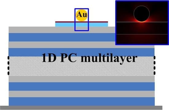
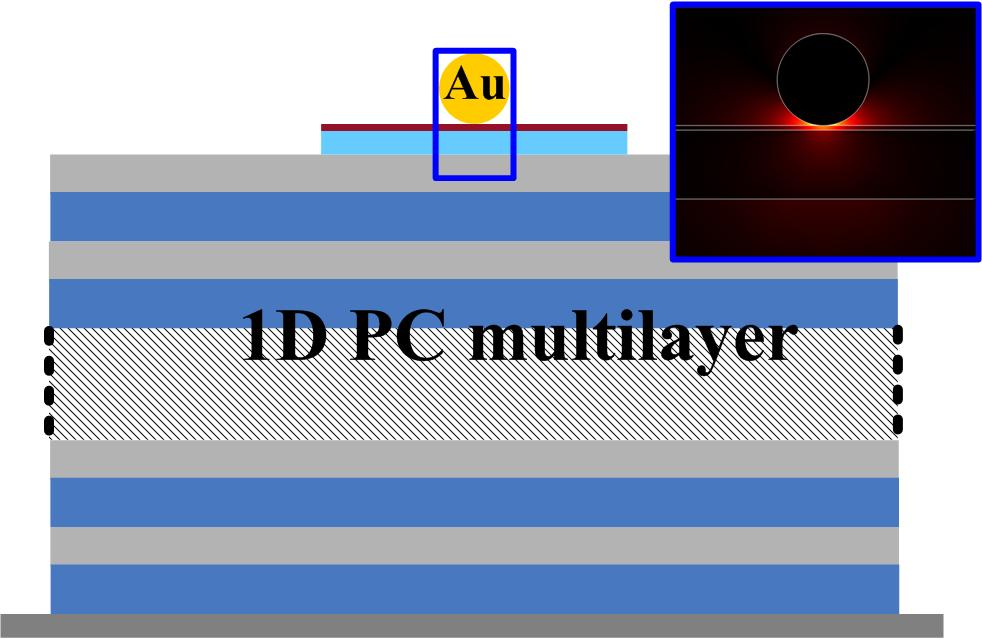
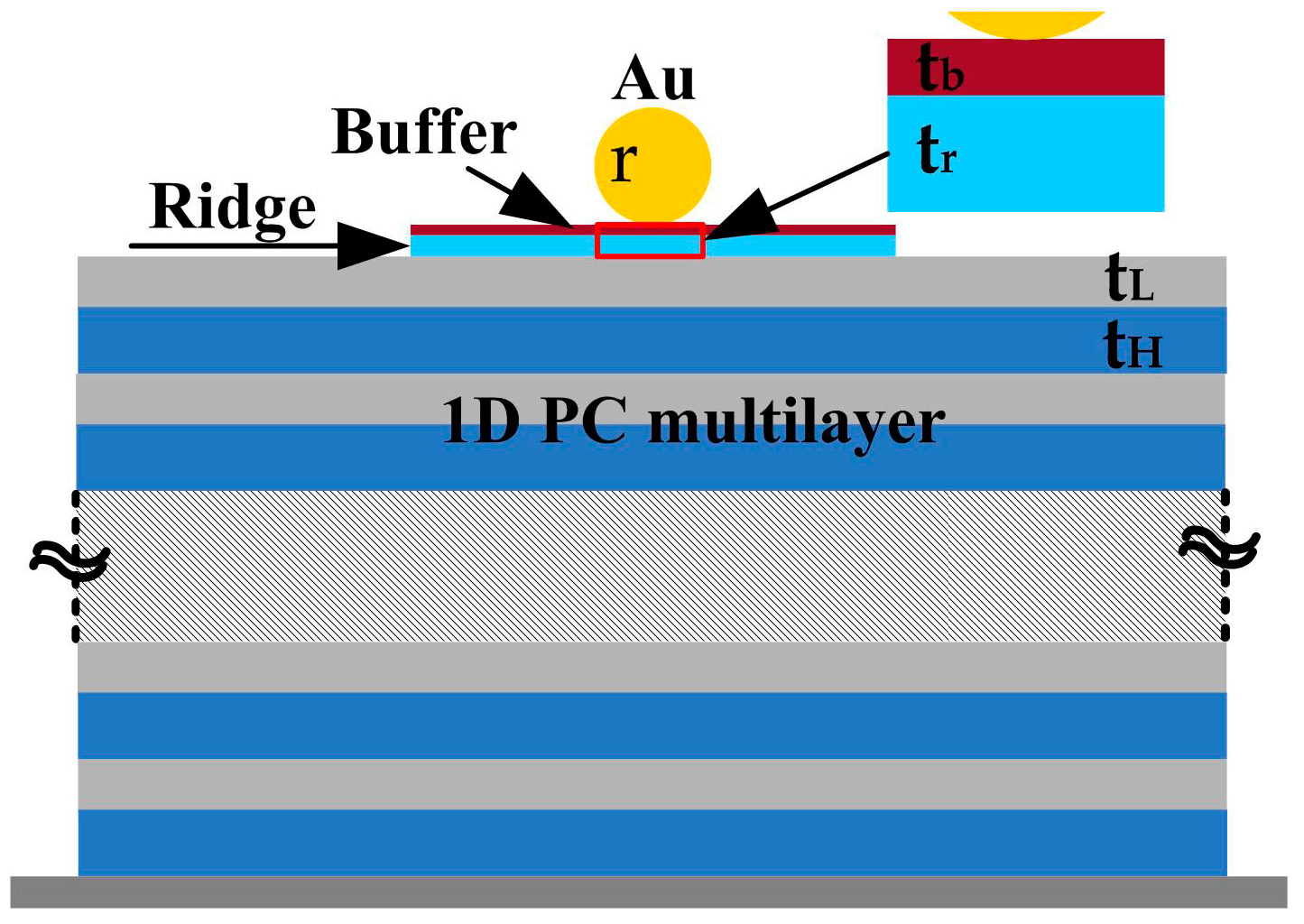
The structure of interest is schematically shown in Figure 1, which consists of a metallic nanowire placed near the up side of a high-index, dielectric-ridge-loaded 1D PC multilayer structure, with a low-index, nanoscale buffer layer sandwiched between them. The metallic nanowire is buried in air cladding, supporting the subwavelength tightly confined plasmonic mode over a wide wavelength range at the surface. With appropriate design, the BSW mode can be excited in the 1D PC multilayer structures for p-polarized incident light for the considered wavelength. The sandwiched buffer layer helps to squeeze the hybrid optical mode within the nanoscale gap region with low modal loss. The hybridization between the BSP and SPP modes is conducted by tuning the structural parameters of the waveguide.
In our study, the operating wavelength is set at the telecommunication wavelength λ of 1550 nm. The 1D PC multilayer structure consists of 20 alternating TiO2 (H, high-index) and SiO2 (L, low-index) layers, with the thicknesses of tH = 385 nm and tL = 350 nm, respectively. The material of the high-index dielectric ridge is selected as TiO2, the thickness of which is defined as tr and the width of which is 3 μm. The parameters and materials listed above are designed to be able to excite the BSW mode in the truncated 1D PC multilayer structure according to the formula in Reference [21]. The metal nanowire is chosen as gold for its good optical properties and chemical stability with the radius of r. The material of the buffer layer is selected as SiO2, the thickness of which is denoted as tb and the width of which is the same as the dielectric ridge. The refractive indices of TiO2, SiO2, Au, and air at the operating wavelength are nh = 2.438, nl = 1.444, nau = 0.55 + 11.5i and nc = 1, respectively. In the following, the characteristics of the hybrid waveguide are investigated by solving the Helmholtz equation with the finite-element method (FEM) method based on COMSOLTM, the mode analysis is carried out in the frequency domain which belongs to an RF (Radio Frequency) module, and a first-order scattering boundary condition is used in the eigenmode solver.
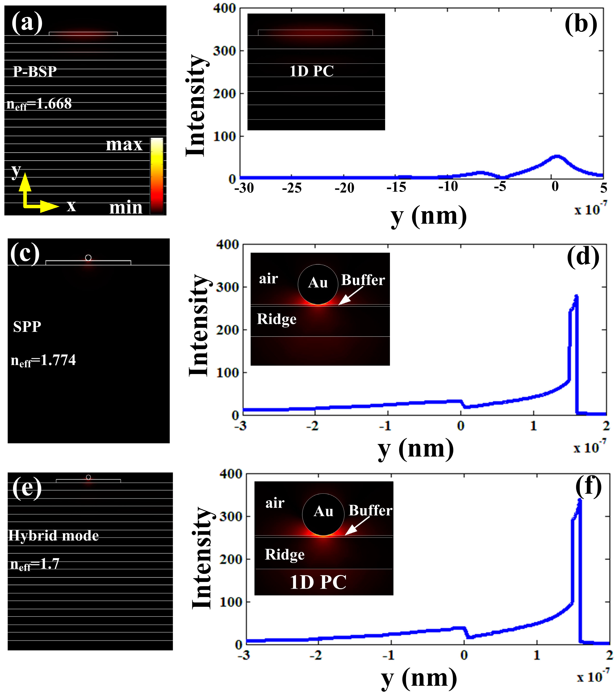
In order to illustrate the local field enhancement of the proposed HBSPP waveguide structure and the hybrid mode, we obtained the result of the coupling between the SPP mode and the BSP mode. The E field distributions are plotted with the same scale and the corresponding effective refractive indices of the SPP that excited with the metal nanowire only, the BSP that excited within the 1D PC only, and the hybrid mode proposed in our paper are respectively marked. The structural parameters of the waveguides are chosen as: tr = 150 nm, tb = 10 nm, and r = 100 nm, respectively. It can be seen in Figure 2 that, for the 1D PC, the enhanced electric field is mostly distributed in the dielectric-ridge layer and the underneath multilayer structure, and the maximum E field enhancement factor is ~50; for the metal nanowire, the E field enhancement factor is ~280. For the hybrid mode, the E field is strongly confined within the gap between the buffer layer and the metal nanowire with a greatly enhanced factor of ~350, which is larger than that of both the SPP mode and BSP mode, and the effective refractive index of the mode is between that of the SPP mode and that of the BSP mode. As far as is observed, the BSP mode and the SPP mode couple with each other and the resulting hybrid mode shows similar characteristics to the SPP mode with a further increased E field enhancement.
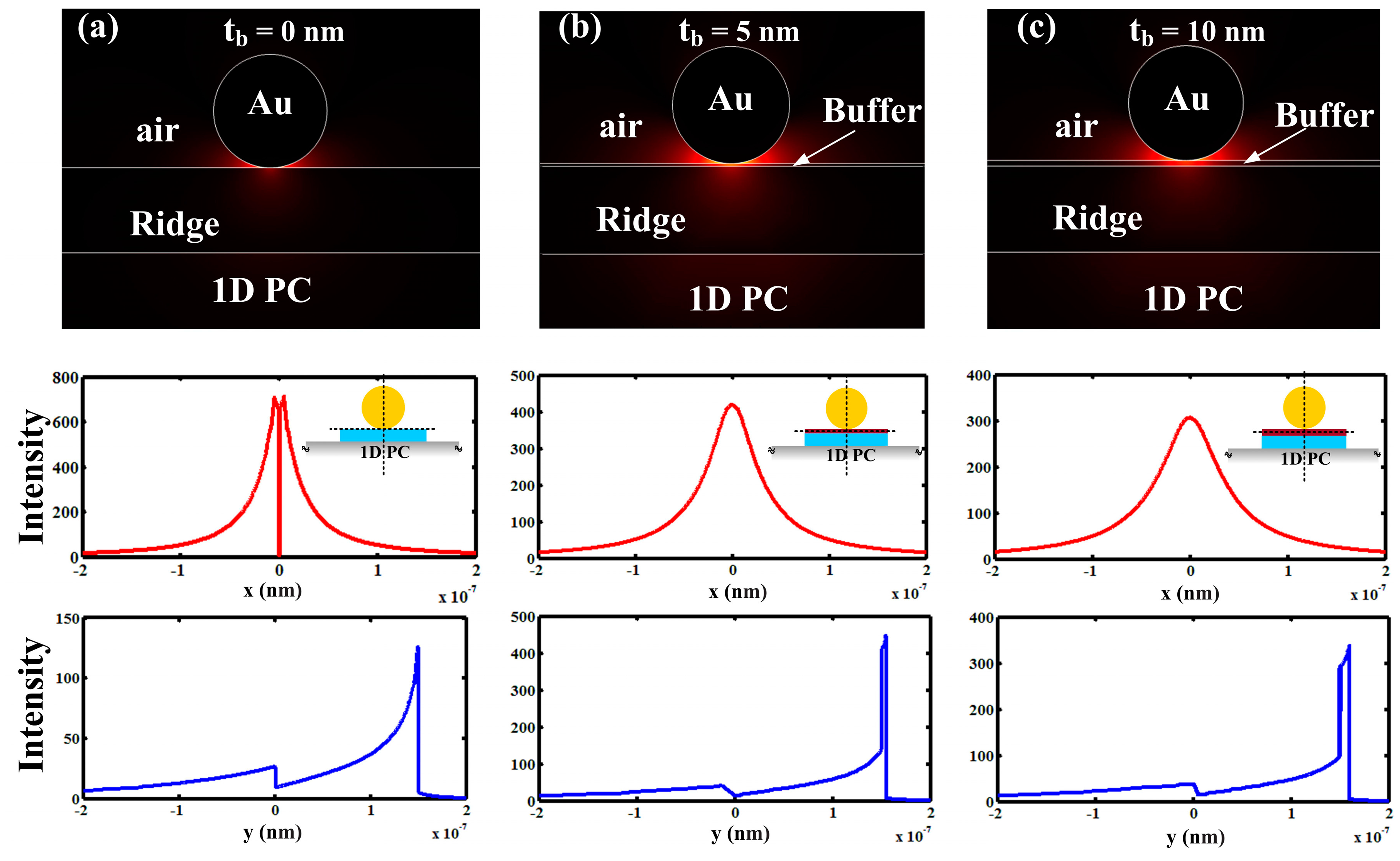
As a simple demonstration, the electric field distributions of the coupling mode supported by the HBSPP waveguide with different buffer layer thicknesses are investigated. The key structural parameters of the hybrid waveguide were chosen as tr = 150 nm, r = 100 nm, respectively. The extreme case corresponding to tb = 0 nm is shown in Figure 3a, where the metal nanowire is put directly on the high-index dielectric ridge. It can be noticed that the electric field is tightly confined at the bottom of the metal nanowire, resulting in an ultra-small mode area. Introducing a low-index buffer layer between the metal nanowire and the dielectric ridge could lead to significant field enhancement and tight optical confinement in the thin buffer layer, as can be seen in Figure 3b,c. Although the squeeze of the field inside the thin buffer layer becomes less significant for the larger thickness, the modal attenuation declines correspondingly, bringing the increment of propagation distance. The simple investigation of the modal properties for the HBSPP waveguide demonstrates that by tuning the gap size, the proposed structure offers possibilities for achieving a large propagation distance in conjunction with tight field localization simultaneously.
3. Optical Properties and Modal Analysis of the Proposed Hybrid Waveguide
In order to quantitatively investigate the proposed HBSPP waveguide′s potential in low-loss light propagation at the subwavelength scale, the dependence of the hybrid modal properties on the thickness of the buffer layer are studied by varying tb. The considered key parameters of the guided optical hybrid mode usually include the modal effective refractive index (neff), the propagation length (L), the normalized mode area (Aeff/A0), and the confinement factor (Γ). The propagation length is obtained by L = λ/[4πIm(neff)], which is determined by the effective propagation loss of the mode. The effective mode area Aeff is calculated using [45]:
where, in order to exactly evaluate the energy in the metallic region, the electromagnetic energy density is defined as:
where E(r) and H(r) are the electric and magnetic fields, respectively. ε(r) is the electric permittivity and µ0 is the vacuum magnetic permeability. A0 is the diffraction-limited mode area, defined as λ2/4. Thus, the mode confinement factor is defined as the ratio of the power confined in the considered gap region to the total power of the hybrid waveguide.
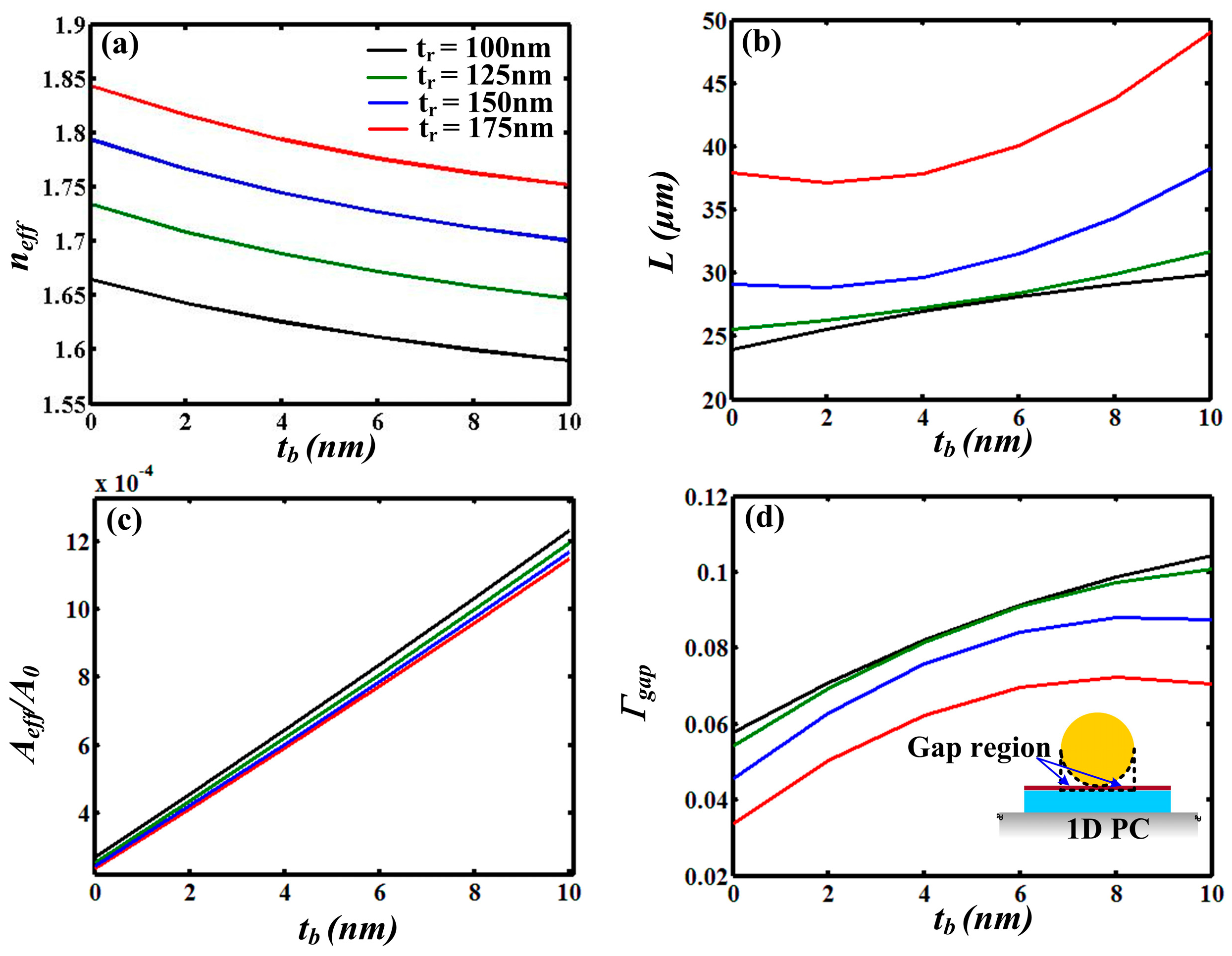
Figure 4 illustrates the variations of the above key characteristics for different thicknesses of the buffer layer when tb varies within the range of 0–10 nm, where the radius of the Au nanowire is fixed at 100 nm for better optical confinement. To control the modal performance, the thickness of the dielectric ridge is set as 100 nm, 125 nm, 150 nm, and 175 nm, respectively. This illustrates the trends of effective refractive index, propagation length, mode area, and confinement factor with the gradual thickening of the buffer layer. It is shown that the strengthened coupling between the metal nanowire and the dielectric-ridge results in deep-subwavelength mode confinement with orders of magnitude enhancement (Aeff/A0 lower than 10−3) (see Figure 4c), while a tens of microns propagation distance can simultaneously be reached within the range of the considered structural parameters. It is worth noting that in spite of the buffer layer being very thin, the optical power confined in the gap region—shown in Figure 4d—is reasonable and could grow larger as the buffer layer thickens further.
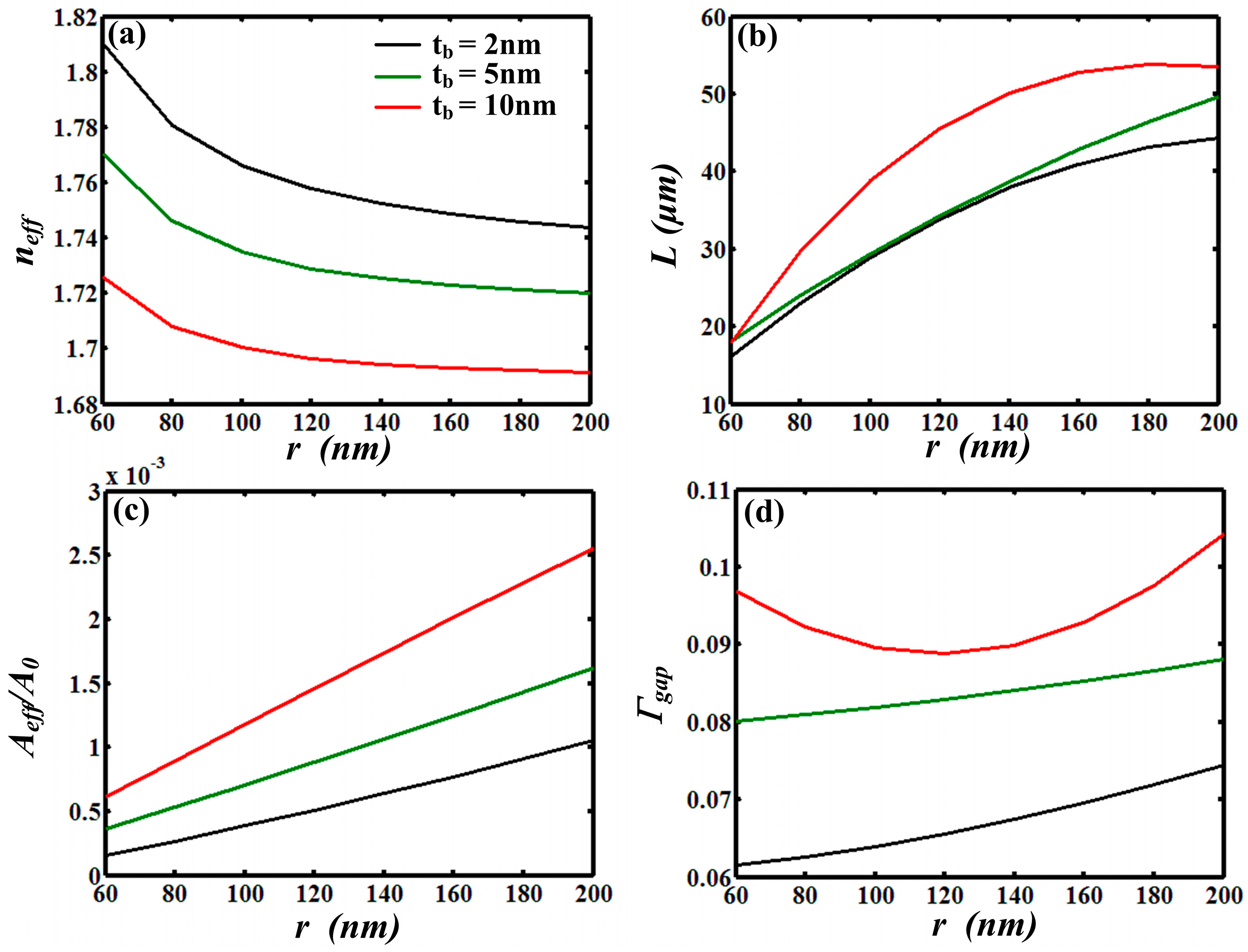
We further investigate the feasibility of controlling the mode properties when the radius of the Au nanowire varies, whereas the thickness of the dielectric ridge is fixed at 150 nm to ensure relatively strong interaction between the BSP mode and SPP mode with low propagation loss and subwavelength mode confinement. Figure 5 shows the calculated results for different buffer thicknesses when the radius of the metallic nanowire varies from 60 nm to 200 nm. It can be observed that with the increment of the radius of the metallic nanowire (r), the propagation length (see Figure 5b) can reach up to tens of micrometers and can be further increased under different buffer thicknesses (tb). Although the mode confinement decreases as the nanowire grows larger, the calculated effective mode area—shown in Figure 5c—can still maintain a deep-subwavelength scale with Aeff/A0 lower than 10−3. The calculations further reveal that the power confined in the considered region is reasonable and relatively stable with the change of the metallic nanowire radius.
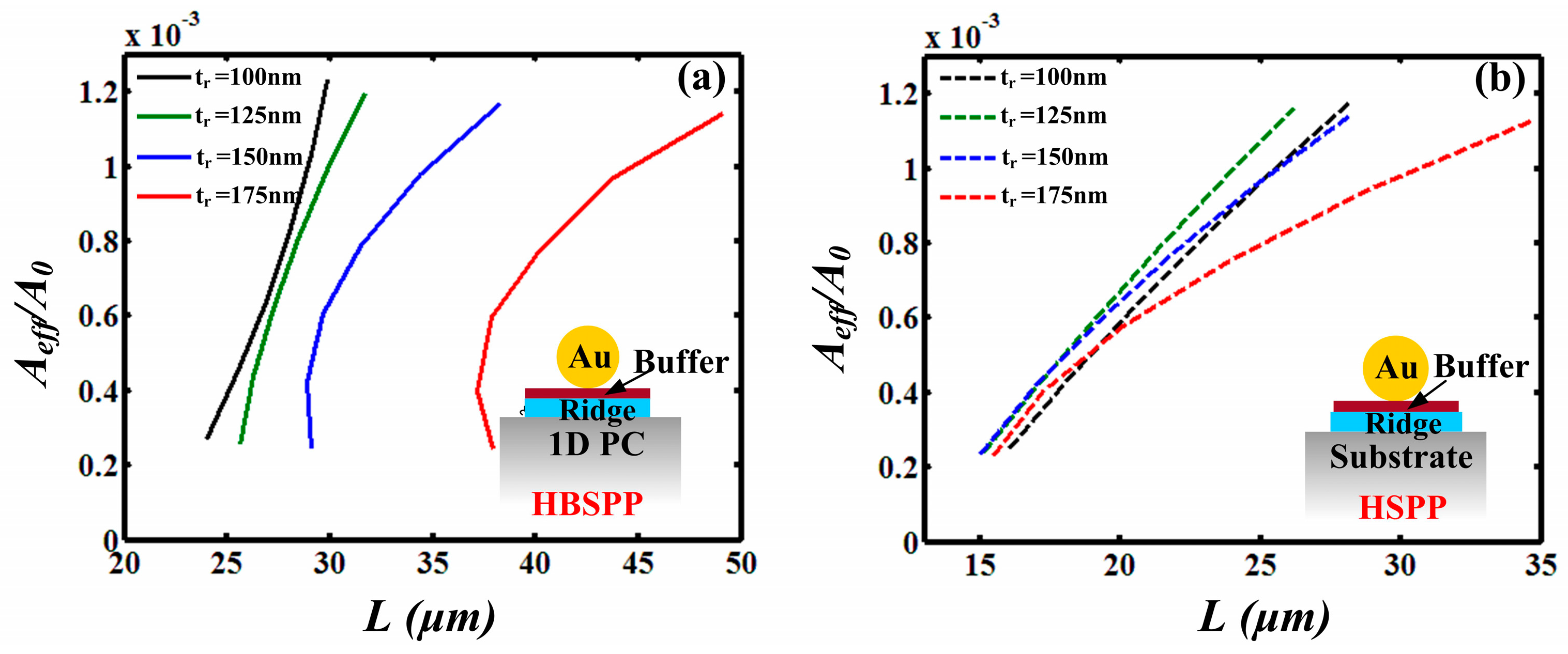
To further benchmark the properties of the proposed hybrid waveguide structure, the quantitative comparison of key parameters such as propagation length and effective mode area between the proposed HBSPP waveguide and a typical hybrid surface plasmon polariton (HSPP) waveguide structure is carried out simultaneously. As is known, the excitation of the BSP mode is based on the internal reflection and refraction of the 1D PC multilayer structures, resulting in a weak confinement of the optical mode. Meanwhile, owing to the absence of metal, the excited low-loss BSP mode in the all-dielectric structure improves the propagation distance dramatically. Therefore, the hybridization of the BSP mode with the SPP mode effectively provides a good propagation distance with strong mode confinement. For fair comparison, the HSPP waveguide structure consists of a nanowire topped on the high-index dielectric ridge with the low-index buffer layer sandwiched between them, as shown in the inset of Figure 6b. The structural parameters and materials of the HSPP waveguide are the same as the proposed HBSPP waveguide, with the absence of the periodical 1D PC. During the comparison, the thickness of the buffer layer is changed to calculate the propagation length (L) and the normalized mode area (Aeff/A0). For intuitive comparison of the modal properties, the 2D plots of the HBSPP waveguide and the HSPP waveguide are depicted in Figure 6a,b, respectively. The results of the HSPP waveguide are calculated using the same method as the proposed HBSPP waveguide shown above. As clearly illustrated in Figure 6, for the proposed hybrid waveguide, a ~2 times larger propagation length of the proposed HBSPP waveguide can be achieved compared to that of the HSPP waveguide, although the effective mode area of the HBSPP waveguide increases slightly compared to the corresponding HSPP counterparts. The results indicate that the hybridization of the BSP mode with the SPP mode could help to reduce the propagation loss with a certain sacrifice in the mode confinement.
4. Conclusions
In summary, we have proposed a Bloch-surface-polariton-based hybrid nanowire structure where a metallic nanowire lies upon a truncated periodic multilayer substrate. By introducing a thin buffer layer with low refractive index, hybridization between the SPP in the metallic nanowire and the BSP in the all-dielectric multilayer structure is observed. With the effect of the metallic nanowire, the hybrid mode is confined more tightly compared to the BSP. As the hybrid mode is still mostly confined in the dielectric, the optical loss is much lower than both the conventional SPP mode and the hybrid SPP mode. Here, a subwavelength mode confinement is presented with a much lower propagation loss, which results in a ~2 times longer propagation distance compared to a typical hybrid SPP mode. These results could pave the way for the design and realization of BSW-based highly integrated photonic devices.
Acknowledgments
This work has been supported by the National Natural Science Foundation of China (NSFC) (61775009/61505145/61521091/61205078).
Author Contributions
Weijing Kong, Yuhang Wan, and Zheng Zheng conceived and designed the hybrid waveguide structure; Weijing Kong performed the simulation; Wenhui Zhao analyzed the data; Shuna Li contributed analysis tools; Weijing Kong and Yuhang Wan wrote the paper.
Conflicts of Interest
The authors declare no conflict of interest.
References
- Han, Z.; Bozhevolnyi, S. Waveguiding with Surface Plasmon Polaritons. Rep. Prog. Phys. 2014, 76, 016402. [Google Scholar] [CrossRef] [PubMed]
- Gosciniak, J.; Volkov, V.; Bozhevolnyi, S.; Markey, L.; Massenot, S.; Dereux, A. Fiber-coupled dielectric-loaded plasmonic waveguides. Opt. Express 2010, 18, 5314–5319. [Google Scholar] [CrossRef] [PubMed]
- Rukhlenko, I.D.; Premaratne, M.; Agrawal, G.P. Guided plasmonic modes of anisotropic slot waveguides. Nanotechnology 2012, 23, 444006. [Google Scholar] [CrossRef] [PubMed]
- Takahara, J.; Yamagishi, S.; Taki, H.; Morimoto, A.; Kobayashi, T. Guiding of a one-dimensional optical beam with nanometer diameter. Opt. Lett. 1997, 22, 475–477. [Google Scholar] [CrossRef] [PubMed]
- Wei, H.; Zhang, S.; Tian, X.; Xu, H. Highly tunable propagating surface plasmons on supported silver nanowires. Proc. Natl. Acad. Sci. USA 2013, 110, 4494–4499. [Google Scholar] [CrossRef] [PubMed]
- Maier, S.; Kik, P.; Atwater, H.; Meltzer, S.; Harel, E.; Koel, B.; Requicha, A.A.G. Local detection of electromagnetic energy transport below the diffraction limit in metal nanoparticle plasmon waveguides. Nat. Mater. 2003, 2, 229–232. [Google Scholar] [CrossRef] [PubMed]
- Berini, P. Long-range surface plasmon polaritons. Adv. Opt. Photonics 2009, 1, 484–588. [Google Scholar] [CrossRef]
- Krasavin, A.V.; Zayats, A.V. Passive photonic elements based on dielectric-loaded surface plasmon polariton waveguides. Appl. Phys. Lett. 2007, 90, 211101. [Google Scholar] [CrossRef]
- Dionne, J.A.; Sweatlock, L.A.; Atwater, H.A. Plasmon slot waveguides: Towards chip-scale propagation with subwavelength-scale localization. Phys. Rev. B 2006, 73, 035407. [Google Scholar] [CrossRef]
- Guo, X.; Qiu, M.; Bao, J.; Wiley, B.J.; Yang, Q.; Zhang, X. Direct coupling of plasmonic and photonic nanowires for hybrid nanophotonic components and circuits. Nano Lett. 2009, 9, 4515. [Google Scholar] [CrossRef] [PubMed]
- Ditlbacher, H.; Hohenau, A.; Wagner, D.; Kreibig, U.; Rogers, M.; Hofer, F.; Aussenegg, F.R.; Krenn, J.R. Silver nanowires as surface plasmon resonators. Phys. Rev. Lett. 2005, 95, 257403. [Google Scholar] [CrossRef] [PubMed]
- Wei, H.; Wang, Z.; Tian, X.; Käll, M.; Xu, H. Cascaded logic gates in nanophotonic plasmon networks. Nat. Commun. 2011, 2, 387. [Google Scholar] [CrossRef] [PubMed]
- Wu, X.; Xiao, Y.; Meng, C.; Zhang, X.; Yu, S.; Wang, Y.; Yang, C.; Guo, X.; Ning, C.Z.; Tong, L. Hybrid photon-plasmon nanowire lasers. Nano Lett. 2013, 13, 5654–5659. [Google Scholar] [CrossRef] [PubMed]
- Zou, C.L.; Sun, F.W.; Xiao, Y.F.; Dong, C.H.; Chen, X.D.; Cui, J.M. Plasmon modes of silver nanowire on a silica substrate. Appl. Phys. Lett. 2010, 97, 189. [Google Scholar] [CrossRef]
- Li, Z.P.; Bao, K.; Fang, Y.R.; Guan, Z.Q.; Halas, N.J.; Nordlander, P. Effect of a proximal substrate on plasmon propagation in silver nanowires. Phys. Rev. B 2010, 82, 2762–2768. [Google Scholar] [CrossRef]
- Wang, Y.; Ma, Y.; Guo, X.; Tong, L. Single-mode plasmonic waveguiding properties of metal nanowires with dielectric substrates. Opt. Express 2012, 20, 19006–19015. [Google Scholar] [CrossRef] [PubMed]
- Wei, W.; Zhang, X.; Yu, H.; Huang, Y.; Ren, X. Plasmonic waveguiding properties of the gap plasmon mode with a dielectric substrate. Photonics Nanostruct. 2013, 11, 279–287. [Google Scholar] [CrossRef]
- Zhang, S.; Xu, H. Optimizing substrate-mediated plasmon coupling toward high-performance plasmonic nanowire waveguides. ACS Nano 2012, 6, 8128–8135. [Google Scholar] [CrossRef] [PubMed]
- Bian, Y.; Zheng, Z.; Zhao, X.; Liu, L.; Liu, J.; Zhu, J. Nanowire based hybrid plasmonic structures for low-threshold lasing at the subwavelength scale. Opt. Commun. 2013, 287, 245–249. [Google Scholar] [CrossRef]
- Bian, Y.; Gong, Q. Metallic-nanowire-loaded silicon-on-insulator structures: A route to low-loss plasmon waveguiding on the nanoscale. Nanoscale 2015, 7, 4415–4422. [Google Scholar] [CrossRef] [PubMed]
- Yariv, A.; Hong, C.S.; Yeh, P. Electromagnetic propagation in periodic stratified media. I. General theory*. Opt. Soc. Am. 1977, 67, 423–438. [Google Scholar] [CrossRef]
- Yeh, P.; Yariv, A.; Cho, A.Y. Optical surface waves in periodic layered media. Appl. Phys. Lett. 1978, 32, 104–105. [Google Scholar] [CrossRef]
- Meade, R.D.; Brommer, K.D.; Rappe, A.M.; Joannopoulos, J.D. Electromagnetic bloch waves at the surface of a photonic crystal. Phys. Rev. B Condensed Matter 1991, 44, 10961–10964. [Google Scholar] [CrossRef]
- Robertson, W.M. Experimental measurement of the effect of termination on surface electromagnetic waves in one-dimensional photonic bandgap arrays. J. Lightwave Technol. 1999, 17, 2013–2017. [Google Scholar] [CrossRef]
- Shinn, M.; Robertson, W.M. Surface plasmon-like sensor based on surface electromagnetic waves in a photonic band-gap material. Sens. Actuators B Chem. 2005, 105, 360–364. [Google Scholar] [CrossRef]
- Sinibaldi, A.; Danz, N.; Descrovi, E.; Munzert, P.; Schulz, U.; Sonntag, F. Direct comparison of the performance of bloch surface wave and surface plasmon polariton sensors. Sens. Actuators B Chem. 2012, 174, 292–298. [Google Scholar] [CrossRef]
- Hsu, Y.C.; Chen, L.W. Bloch surface wave excitation based on coupling from photonic crystal waveguide. J. Opt. 2010, 12, 095709. [Google Scholar] [CrossRef]
- Descrovi, E.; Sfez, T.; Quaglio, M.; Brunazzo, D.; Dominici, L.; Michelotti, F. Guided bloch surface waves on ultrathin polymeric ridges. Nano Lett. 2010, 10, 2087–2091. [Google Scholar] [CrossRef] [PubMed]
- Sfez, T.; Descrovi, E.; Yu, L.; Brunazzo, D.; Quaglio, M.; Dominici, L.; Nakagawa, W.; Michelotti, F.; Giorgis, F.; Martin, O.J.F.; et al. Bloch surface waves in ultrathin waveguides: Near-field investigation of mode polarization and propagation. J. Opt. Soc. Am. B 2010, 27, 1617–1625. [Google Scholar] [CrossRef]
- Giorgis, F.; Descrovi, E.; Summonte, C.; Dominici, L.; Michelotti, F. Experimental determination of the sensitivity of bloch surface waves based sensors. Opt. Express 2010, 18, 8087–8093. [Google Scholar] [CrossRef] [PubMed]
- Paeder, V.; Musi, V.; Hvozdara, L.; Herminjard, S.; Herzig, H.P. Detection of protein aggregation with a bloch surface wave based sensor. Sens. Actuators B Chem. 2011, 157, 260–264. [Google Scholar] [CrossRef]
- Konopsky, V.N.; Alieva, E.V. A biosensor based on photonic crystal surface waves with an independent registration of the liquid refractive index. Biosens. Bioeletron. 2010, 25, 1212–1216. [Google Scholar] [CrossRef] [PubMed]
- Sinibaldi, A.; Rizzo, R.; Figliozzi, G.; Descrovi, E.; Danz, N.; Munzert, P. A full ellipsometric approach to optical sensing with bloch surface waves on photonic crystals. Opt. Express 2013, 21, 23331–23344. [Google Scholar] [CrossRef] [PubMed]
- Baryshev, A.V.; Merzlikin, A.M. Approach to visualization of and optical sensing by Bloch surface waves in noble or base metal-based plasmonic photonic crystal slabs. Appl. Opt. 2014, 53, 3142–3146. [Google Scholar] [CrossRef] [PubMed]
- Kong, W.; Wan, Y.; Zheng, Z.; Zhao, X.; Liu, Y.; Bian, Y. High-sensitivity sensing based on intensity-interrogated bloch surface wave sensors. Sens. Actuators B Chem. 2014, 193, 467–471. [Google Scholar] [CrossRef]
- Descrovi, E.; Frascella, F.; Sciacca, B.; Geobaldo, F.; Dominici, L.; Michelotti, F. Coupling of surface waves in highly defined one-dimensional porous silicon photonic crystals for gas sensing applications. Appl. Phys. Lett. 2007, 91, 1987. [Google Scholar] [CrossRef]
- Kong, W.; Wan, Y.; Ni, X.; Zhao, W.; Li, S.; Zheng, Z. Optimizing loss of the dielectric stack for Bloch-surface-wave sensors under different interrogation schemes. J. Mod. Opt. 2017, 64, 407–412. [Google Scholar] [CrossRef]
- Wan, Y.H.; Zheng, Z.; Kong, W.J.; Zhao, X.; Liu, J.S. Fiber-to-fiber optical switching based on gigantic bloch-surface-wave-induced goos–hanchen shifts. IEEE Photonics J. 2013, 5, 7200107. [Google Scholar] [CrossRef]
- Olivieri, A.; Lisickaskrzek, E.; Northfield, H.; Liscidini, M.; Menotti, M.; Tait, N.; Fong, N.; Berini, P. Bloch long-range surface plasmon polaritons in metallic stripe waveguides. CLEO Sci. Innov. 2017. [Google Scholar] [CrossRef]
- Fornasari, L.; Floris, F.; Patrini, M.; Canazza, G.; Guizzetti, G.; Comoretto, D. Fluorescence excitation enhancement by bloch surface wave in all-polymer one-dimensional photonic structure. Appl. Phys. Lett. 2014, 105, 117_1–117_500. [Google Scholar] [CrossRef]
- Toma, K.; Descrovi, E.; Toma, M.; Ballarini, M.; Mandracci, P.; Giorgis, F. Bloch surface wave-enhanced fluorescence biosensor. Biosens. Bioeletron. 2013, 43, 108–114. [Google Scholar] [CrossRef] [PubMed]
- Ballarini, M.; Frascella, F.; Michelotti, F.; Digregorio, G.; Rivolo, P.; Paeder, V.; Musi, V.; Giorgis, F.; Descrovi, E. Bloch surface waves-controlled emission of organic dyes grafted on a one-dimensional photonic crystal. Appl. Phys. Lett. 2011, 99, 144. [Google Scholar] [CrossRef]
- Fornasari, L.; Floris, F.; Patrini, M.; Comoretto, D.; Marabelli, F. Demonstration of fluorescence enhancement via bloch surface waves in all-polymer multilayer structures. Phys. Chem. Chem. Phys. 2016, 18, 14086–14093. [Google Scholar] [CrossRef] [PubMed]
- Wan, Y.H.; Zheng, Z.; Shi, X.G.; Bian, Y.S.; Liu, J.S. Hybrid plasmon waveguide leveraging Bloch surface polaritons for sub-wavelength confinement. Sci. China Technol. Sci. 2013, 56, 567–572. [Google Scholar] [CrossRef]
- Bartal, G.; Oulton, R.F.; Sorger, V.J.; Zhang, X. A Hybrid Plasmonic Waveguide for Subwavelength Confinement and Long Range Propagation. Nat. Photonics 2008, 2, 496. [Google Scholar] [CrossRef]
Figure 1.
Schematic diagram of the proposed hybrid waveguide.

Figure 2.
The comparison between the Bloch surface polariton (BSP) mode, the surface plasmon polariton (SPP) mode, and the hybrid mode for p-polarization. Two-dimensional (2D) electric field distributions (a,c,e) and the corresponding one-dimensional (1D) E plot (b,d,f) for the BSP mode, the SPP mode, and the hybrid mode. The structural parameters of the waveguides are chosen as: tr = 150 nm, tb = 10 nm, r = 100 nm.

Figure 3.
(a–c) 2D electric field distributions and the corresponding 1D electric field plots of the excited hybrid modes guided by the hybrid Bloch surface plasmon polariton (HBSPP) waveguide with different buffer layer thicknesses. (a) tb = 0 nm; (b) tb = 5 nm; (c) tb = 10 nm. Other geometric parameters of all these waveguides are chosen as: tr = 150 nm, r = 100 nm. The field profiles are taken at the bottom corner of the Au nanowire for tb = 0 nm, and at the center of the buffer layer for tb = 5 nm and 10 nm.

Figure 4.
Dependence of the proposed modal properties on the buffer layer for different dielectric ridges (r = 100 nm): (a) modal effective index (neff); (b) propagation length (L); (c) normalized mode area (Aeff/A0); (d) confinement factor in the considered gap region (Γgap), which is schematically shown in the inset in (d).

Figure 5.
Dependence of the proposed modal properties on the radius of the metallic nanowire for different buffer layer (tr = 150 nm): (a) modal effective index (neff); (b) propagation length (L); (c) normalized mode area (Aeff/A0); (d) confinement factor in the considered gap region (Γgap) which is schematically shown in the inset in Figure 4d.

Figure 6.
Parametric plots of the normalized mode area (Aeff/A0) versus the propagation length (L) for HBSPP waveguide (a) and a typical hybrid surface plasmon polariton (HSPP) waveguide (b) for both structures, the radius of the Au nanowire is 100 nm, and the thickness of the dielectric ridge is set as 100 nm, 125 nm, 150 nm, and 175 nm, respectively. For a particular dielectric ridge, the thickness of the buffer layer is varied from 0 nm to 10 nm.

© 2018 by the authors. Licensee MDPI, Basel, Switzerland. This article is an open access article distributed under the terms and conditions of the Creative Commons Attribution (CC BY) license (http://creativecommons.org/licenses/by/4.0/).
Share and Cite
MDPI and ACS Style
Kong, W.; Wan, Y.; Zhao, W.; Li, S.; Zheng, Z. Bloch-Surface-Polariton-Based Hybrid Nanowire Structure for Subwavelength, Low-Loss Waveguiding. Appl. Sci. 2018, 8, 358. https://doi.org/10.3390/app8030358
AMA Style
Kong W, Wan Y, Zhao W, Li S, Zheng Z. Bloch-Surface-Polariton-Based Hybrid Nanowire Structure for Subwavelength, Low-Loss Waveguiding. Applied Sciences. 2018; 8(3):358. https://doi.org/10.3390/app8030358
Chicago/Turabian StyleKong, Weijing, Yuhang Wan, Wenhui Zhao, Shuna Li, and Zheng Zheng. 2018. "Bloch-Surface-Polariton-Based Hybrid Nanowire Structure for Subwavelength, Low-Loss Waveguiding" Applied Sciences 8, no. 3: 358. https://doi.org/10.3390/app8030358
Note that from the first issue of 2016, this journal uses article numbers instead of page numbers. See further details here.