Nanometric Plasmonic Rulers Based on Orthogonal Plasmonic Gap Modes in Metal Nanoblocks


Department of Physics, Chung-Ang University, Seoul 06974, Korea
*
Author to whom correspondence should be addressed.
Appl. Sci. 2018, 8(3), 386; https://doi.org/10.3390/app8030386
Submission received: 22 January 2018
/
Revised: 21 February 2018
/
Accepted: 28 February 2018
/
Published: 6 March 2018
(This article belongs to the Special Issue Photonic Metamaterials)
Abstract
:We theoretically propose a three-dimensional (3D) plasmonic ruler based on orthogonal plasmonic gap modes which have different wavelengths. The ruler consists of three silver nanoblocks with two ten-nanometer air gaps. First, in a two-block structure, the lateral displacement of one block can be determined by the absorption spectrum, in which two orthogonal modes are observed with different wavelengths. Secondly, in a three-block structure, due to the distinctive wavelength dependencies on the x- or y-directional movement of the two orthogonal modes and the strong dependencies on the air gap size, the 3D positioning of one nanoblock relative to a reference nanoblock can be measured with a 2.5 nm resolution using the spectral positions of the absorption spectrum.
1. Introduction
Localized surface plasmon resonances of noble metal nanoparticles (e.g., gold and silver) depend on the shape and size of the particles at the visible and infrared wavelength regions [1,2,3,4,5,6,7,8,9,10,11,12,13]. Specifically, because of strong plasmonic coupling at the small air gap between the metal particles, a resonant wavelength of the gap plasmon increases when metal particles are placed close together [1,2,3,4,5].
Plasmonic rulers that have ultrafine sensitivity to the position of the target particle are useful for investigating molecular dynamic processes, such as DNA hybridization, enzyme cleavage, and protein–protein interaction in the real-time monitoring of spectral shifts [6,7,8,9]. Because of the strong gap dependences, most available plasmonic rulers are used to measure a change in distance in one dimension along the gap direction. However, plasmonic rulers have recently been able to achieve three-dimensional (3D) nanometer-scale position monitoring using five gold nanorods and their dipole–quadrupole interactions [10,11]. This advancement provides the opportunity to study 3D molecular dynamics. To take advantage of 3D rulers for biosensors, plasmonic rulers which have a simpler geometry are needed.
In this paper, we propose a 3D plasmonic ruler that achieves a 2.5 nm resolution, which is limited by the numerical precision of the calculation. The resolution can be improved by using a smaller spatial grid in the simulations. The proposed structure consists of three rectangular silver nanoblocks, separated by 10 nm air gaps. In the air gaps, two orthogonal higher-order dipole modes with different wavelengths can be excited by injecting lights with vertical, linear polarization. The proposed 3D plasmonic ruler enables accurate measurements of a nanometer distance change by a single measurement of an absorption spectrum.
2. Two-Dimensional Positioning of a Nanoblock
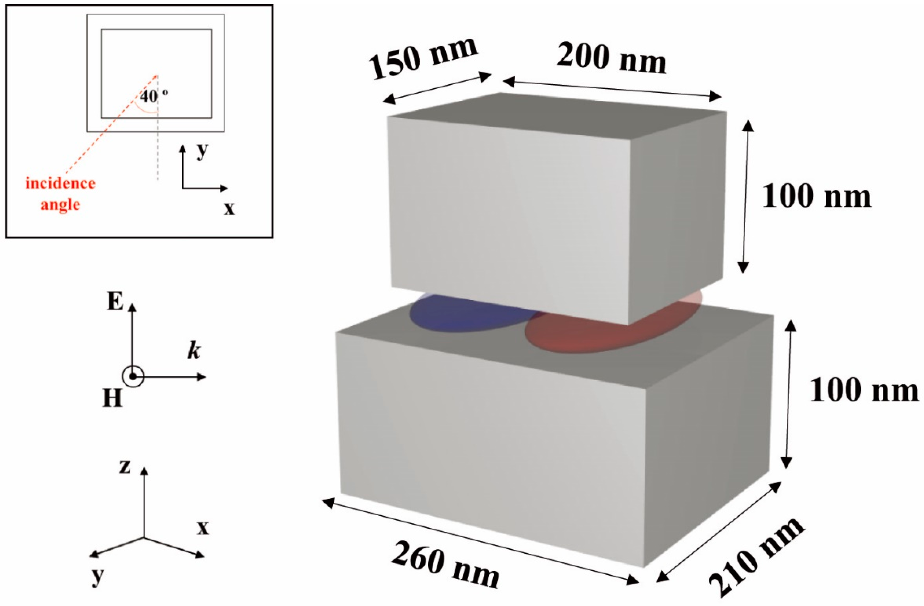
The proposed 3D plasmonic ruler is composed of three silver nanoblocks. In order to readily illustrate the plasmonic interactions between the three blocks, we first investigated the optical properties of simpler structures that consist of two silver nanoblocks, called a 2D plasmonic ruler. After the determination of the lateral movement of two blocks, we extend the concept of the ruler to three silver nanoblocks. Figure 1 shows a schematic diagram of a 2D plasmonic ruler that consists of a large silver nanoblock and a small nanoblock, where the blocks are spaced with an air gap of 10 nm. The upper small nanoblock and the lower large nanoblock have dimensions of 200 nm × 150 nm × 100 nm and 260 nm × 210 nm × 100 nm, respectively. In this structure, the lateral movement along the x–y plane of the upper block is estimated by observing the absorption spectra, and the lower block with a fixed position is declared as the reference block. Silver is an optimal material because of its lower absorption losses in noble metals for the spectral range of interest. The center block size was chosen to locate the spectral positions of plasmon resonant mode 1 (M1) and mode 2 (M2) near 1000 nm. The peak wavelengths are insensitive to the upper and lower block sizes. The given differences in x and y dimensions of the center block were determined for two peaks, M1 and M2, which were placed with enough spectral spacing to be larger than linewidths of the peaks.
In this paper, we calculate higher-order plasmonic resonant modes and their absorption cross-sections using a 3D finite-difference time-domain (FDTD) method. Silver was modeled by the Drude model, which is represented as follows:
The background dielectric constant (), plasma frequency (ωp), and collision frequency (γ) were set to 3.14, 9.13, and 0.021 eV, respectively, by fitting experimentally-determined dielectric functions of silver [14]. The spatial grid along the x, y and z axes were 2.5, 2.5, and 1 nm, respectively.
When an incident light, linearly polarized along the z-axis (Ez), is injected into the proposed structure, a strongly confined surface plasmon cavity mode can be excited in the air gaps between nanoblocks. In this case, there are two orthogonal, higher-order plasmon resonant modes with one intensity node along the x- or y-axis. Moreover, compared with a fundamental gap cavity mode, the proposed cavity modes have one intensity node that suppresses radiation loss along the node direction [15,16]. Suppression of radiation loss provides a narrow linewidth, which can enhance the sensitivity of the gap size sensors [15,16]. Depending on the direction of the incident light, one of two modes can be selected by mode matching with an incident plane wave.
When the linearly polarized light is injected into the proposed structure along the y-axis or x-axis, a plasmon resonant mode 1 (M1) with an intensity node along the x-axis or a mode 2 (M2) with a node along the y-axis can be excited in the air gap between the two nanoblocks, as shown in Figure 2a,b. To estimate the lateral movement (Δx and Δy) of the upper block, we need to exploit the optical properties of the two plasmonic modes, M1 and M2, simultaneously. In order to excite M1 and M2 at the same time, the incident angle of light was set to 40° from the y-axis (see inset of Figure 1). Our modes M1 and M2 have strong electric field in the air gap, not around sharp block edges. Additionally, as shown in the mode profiles of Figure 2, significant enhancements at the edges are not observed. In fact, the resonant wavelengths of M1 and M2 are maintained, except for slight blue-shift due to the decrease of the effective cavity size when the corner of the blocks are rounded. In other words, the proposed plasmonic ruler is robust to the rounding of edges in the realistic experimental nanoparticles.
In spite of the similarity in the mode profiles of M1 and M2, the resonant wavelengths of the two modes are different because of the different x- and y-directional sizes of the rectangular cavity: 200 and 150 nm. Figure 2a,b present a top-view of the dominant electric field (Ez) mode profiles of M1 and M2 when the upper block is placed just above the center of the lower large block, where the profiles are obtained at the center of the air gap. The resonant wavelengths of M1 and M2 are 882.2 and 1081.3 nm, respectively. M2, with an intensity node along the y-axis, primarily oscillates along the x-axis (the longer axis) and has a longer wavelength than that of M1.
Next, we investigate changes in the properties of each mode for a lateral movement of the upper block when the air gap between the upper and lower blocks is fixed. As shown in Figure 2c,d, when the upper block moves on the x- and y-axes by amounts of Δx = 30 nm and Δy = 30 nm from the original position, the position of the strongly confined field also changes with respect to the upper block position. Therefore, an effective cavity size that determines a resonant wavelength of a cavity mode can be changed because the electric field of the cavity mode partially experiences the placement of the air region out of the lower block. In this regard, M1 and M2 experience distinct resonant wavelength shifts depending on the direction and size of the lateral displacements, Δx or Δy, of the upper block. If the changes of the resonant wavelengths of M1 and M2 are measured, the direction and size of the lateral movement of the upper block are also obtained. As a result, the proposed structure can operate as a plasmonic ruler, which enables measurement of the horizontal relative position of the upper block to the lower block.
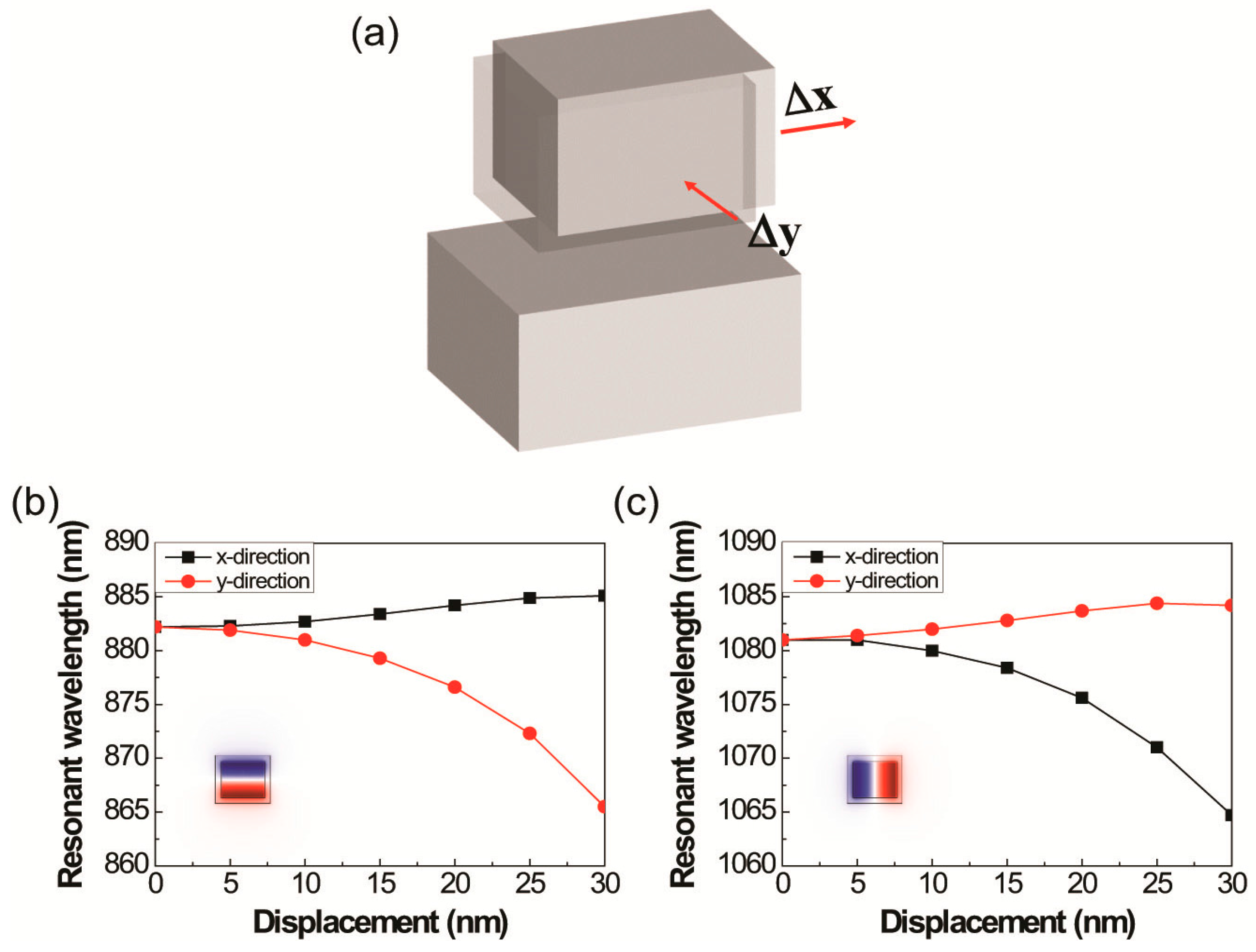
In order to quantify the change in the resonant wavelength of each mode for the lateral movement of the upper block, we calculated the resonant wavelengths of M1 and M2 as functions of the movement of the block along the x- or y-direction from 0 to 30 nm at 5 nm increments. Figure 3a shows a schematic diagram of the upper block movement in the x- and y-directions. In this case, the air gap thickness between the upper and lower blocks was fixed to 10 nm. First, in the case of M1, as shown in Figure 3b, distinctive resonant wavelength shifts are observed depending on the moving direction, x- (black) or y- (red). When the block moves along the x-direction from 0 to 30 nm, the resonant wavelength of the M1 slightly increases from 882.2 to 885.1 nm. In contrast, when the block moves along the y-direction from 0 to 30 nm, the resonant wavelength of M1 largely decreases from 882.2 to 865.1 nm. Hence, the wavelength of M1, with an intensity node along the x-axis, has a larger wavelength shift for the movement of the upper block along the y-axis.
On the other hand, the resonant wavelength of M2 shows opposite dependences on the movement of the block. As demonstrated in Figure 3c, when the upper block moves along the x-direction from 0 nm to 30 nm (black), the resonant wavelength largely blue-shifts from 1081.3 to 1064.7 nm; when the upper block moves along the y-direction (red), the wavelength slightly red-shifts from 1081.3 to 1084.2 nm. The wavelength of M2 with a node along the y-axis has a larger wavelength shift for the movement of the block along the x-axis. That is to say, when the upper block is moved in the node direction, the resonant wavelength is slightly red-shifted; when it is moved perpendicular to the node direction, the resonant wavelength is largely blue-shifted. Based on these different dependences of the changes in wavelengths of the two modes, M1 and M2, we expect that the lateral position of the upper block can be estimated by observing the resonant wavelengths of M1 and M2 simultaneously.
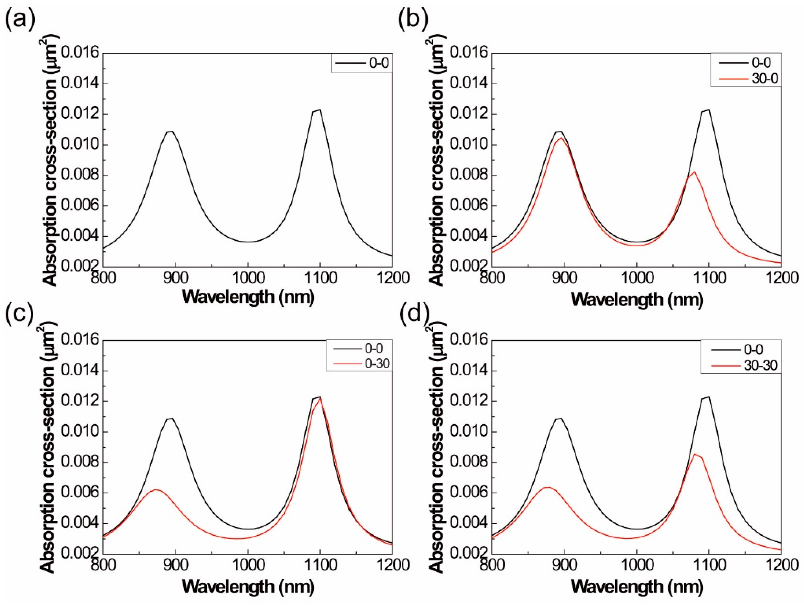
The absorption cross-sections of the cavity structure are strongly enhanced at the resonant wavelength of the plasmonic cavity mode. In order to exploit the absorption cross-section spectra to obtain the resonant wavelength shifts of M1 and M2 for the lateral movement of the upper block, a monochromatic plane wave source with vertical polarization (Ez) was injected into the proposed structure to excite the plasmonic modes M1 and M2 simultaneously. As shown in the inset of Figure 1, the incidence angle of the plane wave was set to 40° and the absorption cross-section was calculated in the spectral range from 800 to 1250 nm, which includes the resonant wavelengths of M1 and M2. Figure 4a shows the absorption cross-section spectrum for the original position of the upper block, indicated by (0-0) meaning (Δx = 0 nm and Δy = 0 nm). In this absorption cross-section spectrum, each peak position corresponds to the resonant wavelengths of M1 and M2 (882.2 and 1081.3 nm, respectively). Similarly, Figure 4b–d show the absorption cross-section spectra for the lateral movement of the upper block: (30-0), (0-30), and (30-30), respectively. Black curves represent the absorption cross-section spectrum at the reference position, as shown in Figure 4a, and red curves represent the absorption spectra with respect to the corresponding position of the upper block.
In the case of the movement of the block only along the x-axis by 30 nm (denoted (30-0) in Figure 4b), the corresponding absorption peaks in the red curve are 885.1 and 1064.7 nm, respectively, which correspond to M1 and M2. The shorter wavelength mode, M1, has a small red-shift of 2.9 nm and the longer wavelength mode, M2, has a large blue shift of 16.6 nm. In contrast, for the movement only along the y-axis by 30 nm—(0-30) in Figure 4c—M1 has a large blue-shift of 17.1 nm and M2 has a small red-shift of 2.9 nm. In the case of movement of Δx = 30 nm and Δy = 30 nm, (30-30), the two modes have large blue-shifts of 16.9 and 16.3 nm. Compared to the initial wavelengths, the shifted absorption resonant wavelengths have similar tendencies with the resonant wavelength shifts characteristic of M1 and M2, as depicted in Figure 3b,c. A large wavelength shift of M1 (M2) along the y- (x-)axis exploits the resonant wavelength of M1 (M2) as a ruler for the y- (x-)directional position of the upper block.
The intensity of the mode which has a large wavelength shift for a given movement of the block changes considerably. For example, in Figure 4b, the peak intensity of M2 which shows large wavelength shift decreases from 0.012 to 0.08 in contrast to the no significant change of M1 intensity because light coupling into each mode changes depending on the block positions. In order to calculate the absorption spectra, the absorbed energy in the block is calculated by subtracting the flux of the scattered light from the integrated flux of the incident light at each wavelength.
When the angle of incidence changes, the peak positions and linewidths of M1 and M2 are maintained, while the peak intensities change. For example, in the case of the incidence angle of 0°, along the y-axis, only M1 can be observed and M2 disappears. In contrast, for the incidence angle of 90°, along the x-axis, only M2 is observable. Therefore, in changing the incidence angle, one can excite M1 or M2 separately in the experimental measurement, which allows measurement of the spectral position of each peak more accurately by removing the overlap of peaks, resulting in higher sensitivity. In the experiment, a thin oxide layer could be observed on the surfaces of the silver metal blocks. The layer in the air gap induced a slight red-shift of the wavelength due to an increase of the effective optical path length in the gap; however, the operation mechanism of the 3D plasmonic ruler was maintained, except for the shift.
In order to determine the lateral position of the upper block more precisely via the two absorption peaks M1 and M2, we need to calculate the absorption cross-section peak wavelengths of M1 and M2 for 2D movement of the upper block using 2D color mapping of the wavelengths, as shown in Figure 5a,b. In these 2D maps, the absorption peak wavelengths are displayed as different colors for Δx and Δy, ranging from 0 to 30 nm. In the wavelength map of M1 (Figure 5a), the color of the corresponding wavelength is almost maintained along the x-axis, Δx. However, the color changes dramatically along the y-axis, y-directional movement, Δy, which is demonstrated in Figure 3b and Figure 4. In the case of M2 in Figure 5b, the dependencies are opposite, as shown in Figure 3c and Figure 4. Based on two-color mapping of M1 and M2 for the lateral movement of the upper block, it is simple to determine the position of the block if measuring the absorption cross-section spectrum of the incident light with an incidence angle of 40° and with vertical polarization. The method is as follows:
- Determine the wavelengths of two peaks—M1 and M2—of an absorption cross-section spectrum.
- Draw lines corresponding to the two wavelengths, shorter and longer wavelengths, on the 2D color mapping spaces of M1 and M2 (Figure 5a,b, respectively).
- Determine the corresponding movement of Δx (nm) and Δy (nm) from a point of intersection of the two lines.
For example, in the case of Δx = 0 nm and Δy = 0 nm, the absorption peak wavelengths of M1 and M2 are 882.2 and 1081.3 nm, respectively. The wavelengths are depicted as cyan lines on Figure 5a,b, M1 and M2 mapping. A point of intersection of the two lines is represented as a cyan circle that is almost at Δx = 0 nm and Δy = 0 nm. Similarly, in the case of Δx = 30 nm and Δy = 0 nm, the absorption cross-section peak wavelengths of M1 and M2—885.1 and 1064.7 nm—are drawn as black lines in Figure 5a,b. The intersection, represented by a black circle, is Δx = 29.3 nm and Δy = 0.7 nm, which is the estimated lateral displacement of the upper block. Therefore, the lateral position of the block is precisely determined except for a small discrepancy that results from the finite grid size and the discrete scan step in 2D mapping. Consequently, from a single spectral measurement of two absorption peaks, one can determine the relative lateral displacement of the upper block relative to the reference lower block.
3. Three-Dimensional Positioning of a Nanoblock
Until now, we assumed the air gap thickness to be fixed at 10 nm. However, due to the strong plasmonic coupling in close proximity to metal nanoparticles, the resonant wavelength of the proposed structure has strong gap dependence [1,2,3,4,5,15,16]. For the same structure as is in Figure 3, we calculated the resonant wavelengths of M1 and M2 by varying the vertical position of the upper block along the z-direction, as shown in Figure 6a. The resonant wavelengths of M1 (black) and M2 (red) are plotted as functions of the gap thickness in Figure 6b, with a thickness range from 2 to 20 nm. The wavelengths increase as the gap decreases, and the wavelengths dramatically increase at small gap size. For example, the resonance of M1 red-shifts from 882.2 to 949.2 nm with a change of 66.8 nm; for a decrease of the gap from 10 to 8 nm, there is a change of 2 nm. In contrast, for the same 2 nm change of the gap from 4 to 2 nm, a large red-shift of 359.8 nm is observed from 1164 to 1523.8 nm. This nonlinear dependence of the wavelength on the gap is widely observed in the gap plasmon resonances [1,2,3,4,5]. The wavelength of the two modes, M1 and M2, have similar dependences on gap thickness.
As shown in Figure 5, the lateral displacement of the upper block can be measured precisely using a two-nanoblock structure. However, because of the degrees of freedom in the 3D positioning of a nanoblock relative to the reference block, a combination of lateral and vertical movement cannot be estimated simultaneously in the two-block scheme. Thus, we introduce an extended nanoblock structure that can measure the position of a block three-dimensionally using the same mechanism: the measurement of the absorption peaks of orthogonal plasmonic modes in two silver nanoblocks.
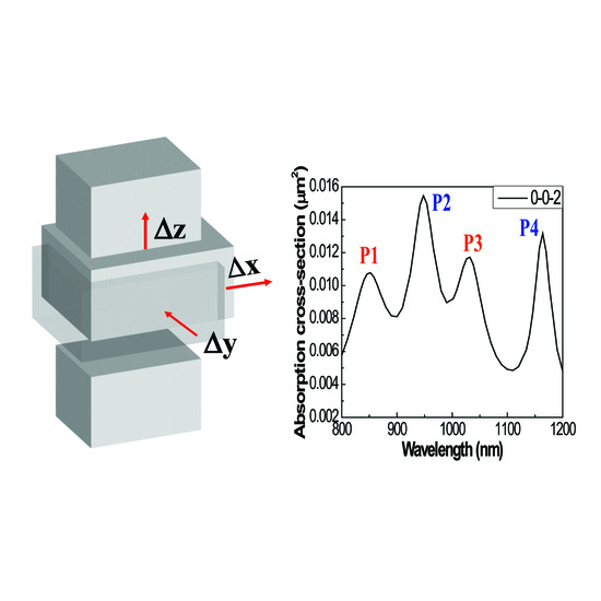
Figure 7a shows the extended nanoblock structure, which consists of three silver nanoblocks. In this structure, we added a small silver nanoblock to the larger block of the two-block structure with the same air gap thickness of 10 nm. Top and bottom small blocks have a size of 200 nm × 150 nm × 100 nm, and the center large block has a size of 260 nm × 210 nm × 100 nm. Contrary to the two-block structure with one air gap, the extended structure consists of two air gaps: between the top small and the center large block, and between the center large and the bottom small blocks. Here, the top and bottom blocks are reference blocks and are assumed to have fixed positions. A center large block is moved three-dimensionally with values of Δx (nm), Δy (nm), and Δz (nm), which is measured by the absorption peaks due to the plasmonic modes in the two air gaps.
First, we calculate the absorption spectrum when the center block is placed at the origin with no movement, Δx = 0 nm, Δy = 0 nm, and Δz = 0 nm, denoted by (0-0-0), as shown in Figure 7b. Because the thicknesses of the two air gaps are the same and both gaps are 10 nm, the absorption cross-section spectrum of the structure shows the same absorption peak wavelengths as those of the two-block structure in Figure 4a: 882.2 and 1081.3 nm, the wavelengths of M1 and M2. However, when the center block moves along the z-axis to 2 nm from the origin, the upper and lower air gaps become 8 and 12 nm, respectively. Due to the strong gap thickness dependence of the resonant wavelengths in the gap plasmonic cavity, as shown in Figure 6b, there are large resonant wavelength differences between the plasmonic modes in the upper and lower air gaps. Figure 7c shows the absorption spectrum of the center block with Δx = 0 nm, Δy = 0 nm, and Δz = 2 nm (the 0-0-2 position). In this figure, there are four absorption peaks at 849.0, 949.2, 1032.3, and 1163.2 nm, which are marked P1, P2, P3, and P4, respectively, from shortest to longest wavelength. P1 (849.0 nm) and P3 (1032.2 nm) indicate the absorption peaks of M1 and M2 excited in the air gap with a thickness of 12 nm, whilst P2 (949.2 nm) and P4 (1163.2 nm) indicate those in the gap with a thickness of 8 nm. The resonant wavelengths can also be confirmed by the curves of the gap dependences of M1 and M2 in Figure 6b.
Next, we investigate the absorption spectrum when the lateral displacement of the center block has a vertical movement of 2 nm. Figure 7d shows the absorption spectrum (red) corresponding to the position of the center block, Δx = 30 nm, Δy = 0 nm, and Δz = 2 nm, denoted by (30-0-2). In comparison with the absorption spectrum of Δx = 0 nm, Δy = 0 nm, and Δz = 2 nm, (0-0-2) (black), P1 and P2 corresponding to the M1 peaks of the air gap of 12 and 8 nm, respectively, are slightly red-shifted, and P3 and P4 corresponding to the M2 peaks of the air gap of 12 and 8 nm are largely blue-shifted. Wavelength shifts in M1 and M2 in the x-directional movement of 30 nm are identical to the wavelength dependences of M1 and M2 in the two-block structure, as shown in Figure 4b. Therefore, we can precisely estimate the position of the center block three-dimensionally using the single absorption spectrum of the three-block structure. On the other hand, four peaks—M1 and M2 modes for upper and lower air gaps—exist independently without any hybridization of each mode. Because M1 and M2 in the same air gap are orthogonal, the two M1 or M2 modes excited in different air gaps cannot couple each other due to large the block height of 100 nm.
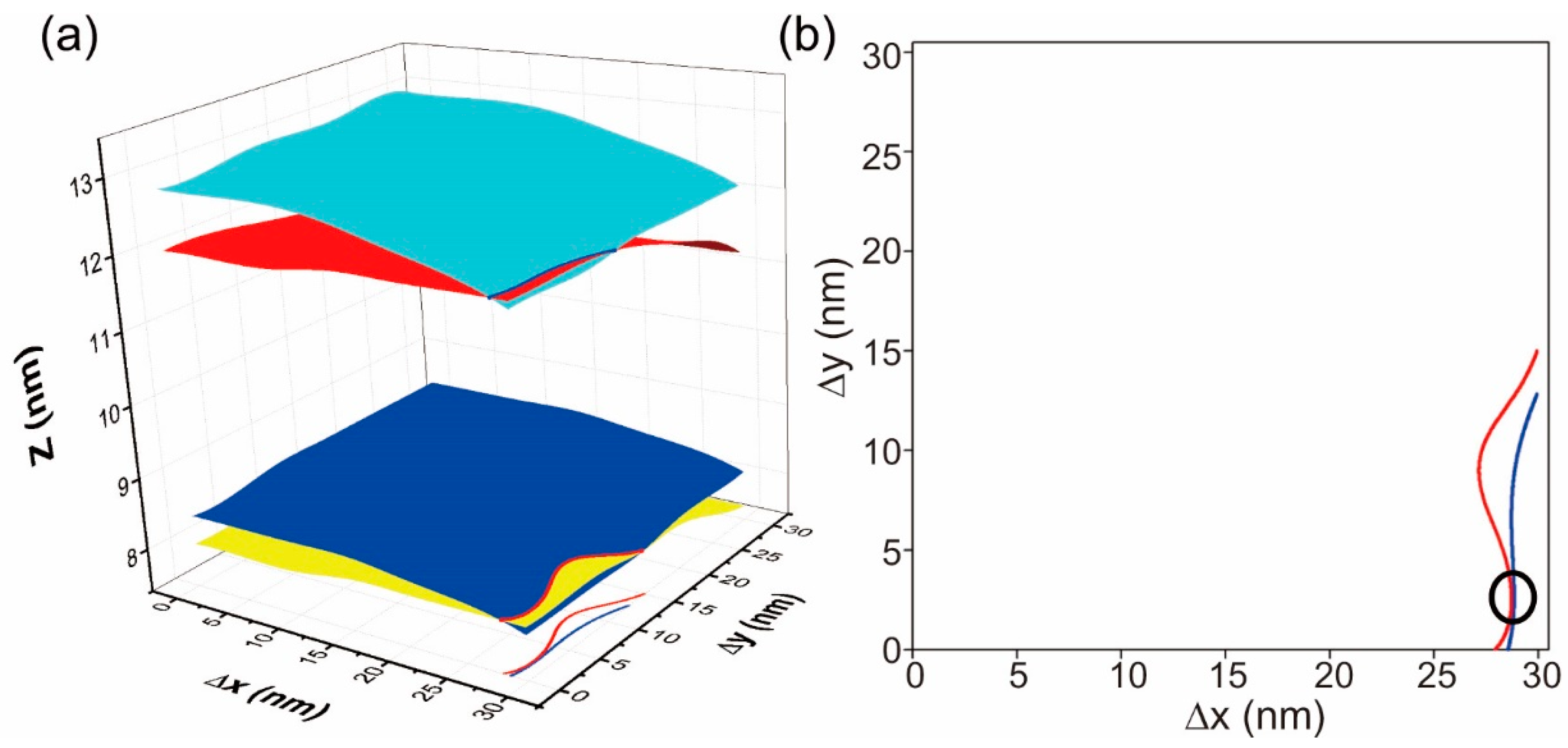
The method of estimating the position of the center block from the absorption spectrum of the three-block structure is analogous to that of the two-block structure. From the absorption spectra (e.g., those in Figure 7c,d), the wavelengths of the four peaks are determined as P1, P2, P3, and P4. Similar to the 2D color map of the wavelengths of M1 and M2 in Figure 5, the absorption peak wavelengths of M1 and M2 in an air gap can be calculated for all of the 3D space of Δx and Δy and for Δz (the air gap thickness). For 3D mapping of the absorption peak wavelengths, the wavelength surfaces for P1 and P2 are plotted in the M1 mapping. In addition, the wavelength surfaces for P3 and P4 are plotted in the M2 mapping.
For example, in the absorption spectrum for the position of the center block, Δx = 30 nm, Δy = 0 nm, and Δz = 2 nm (30-0-2), P1 (852.1 nm), P2 (953.3 nm), P3 (1017.5 nm), and P4 (1148.3 nm) are observed. In Figure 8a, the wavelength surfaces of P1 (red) and P2 (yellow) are plotted on the M1 mapping, and the surfaces of P3 (cyan) and P4 (blue) are plotted on the M2 mapping. Once the surfaces of P1 and P3 are obtained for the same air gap, a blue line—the line of the intersection of P1 and P3 surfaces—can be displayed, which is on the plane of z = 12 nm. Additionally, a red line—the intersection of the surfaces P2 and P4—can be drawn in the plane of z = 8 nm. Based on the planes of the red and blue lines, one can conclude that the vertical position of the center block is moved 2 nm from the original position.
Next, these lines are projected onto the x–y plane and the point of intersection of the two lines indicates the lateral position of the center block. Figure 8 represents an orthographic projection of the blue and red lines onto the x–y plane. In this figure, the intersection of the two lines is indicated by a black circle and is at Δx = 28.7 nm and Δy = 2.2 nm. Finally, the position of the center block is estimated to be (Δx = 28.7 nm, Δy = 2.2 nm, Δz = 2 nm). As a result, the position of the center block can be estimated three-dimensionally using the spectral positions of the four peaks in the absorption spectrum and the calculated 3D mappings of the resonant wavelengths of M1 and M2 in the proposed structure. As mentioned previously, the small discrepancy results from the finite grid size and the discrete scan step in 3D mappings.
The method to determine 3D position of the block is as follows:
- One prepares two 3D wavelength maps of M1 and M2 in 3D spaces of Δx, Δy, and Δz by calculating the wavelengths of M1 and M2 for all positions of the center blocks. The wavelengths of M1 and M2 are 882.2 and 1081.3 nm at origin, Δx = 0 nm, Δy = 0 nm, and z = 10 nm. One wavelength of M1 or M2 is plotted as an equi-wavelength surface in 3D space, such as the equi-wavelength lines of Figure 5. For a certain wavelength of a mode, only one equi-wavelength surface exists in a M1 or M2 3D map. At each z position, the cross-sectional maps in the x–y plane correspond similarly to the 2D color mapping of the wavelengths shown in Figure 5.
- By measuring the absorption spectrum, the spectral positions of four peaks that are two short wavelength peaks are obtained: M1 modes of upper and lower gaps and two long wavelength peaks, and M2 modes of upper and lower gaps. Based on the four wavelengths and the two M1 and M2 wavelength maps in step 1, two M1 equi-wavelength surfaces are plotted on the M1 3D surfaces, and two M2 surfaces are plotted on the M2 3D surfaces similar to the two wavelength lines in the 2D color maps of Figure 5.
- One overlaps four equi-wavelength surfaces on a 3D space and obtains two lines from two intersections of M1 and M2 equi-wavelength surfaces. One set of M1 and M2 surfaces can make only a single intersection line, as shown in the red and blue lines in Figure 8a.
- Determine Δx and Δy of the center block by finding the intersection of two lines in 2D space of Δx and Δy. Based on the determined values of Δx and Δy and the four equi-wavelength surfaces in 3D spaces obtained in step 3, the vertical position, z, of the center block can be determined.
4. Conclusions
We propose a simple 3D plasmonic ruler consisting of three silver nanoblocks: two small blocks (200 nm × 150 nm × 100 nm) and one large block (260 nm × 210 nm × 100 nm), placed with 10 nm-thick air gaps. Because of the different size of the x- and y-directions of the block, two orthogonal plasmonic modes are excited in the air gaps. By measuring the wavelengths of the absorption peaks corresponding to the modes, one can determine the lateral displacement and the vertical movement of the center large block relative to the two small reference blocks due to the distinctive dependences of the two orthogonal modes on x- and y-direction displacement and the strong dependences on air gap size. The proposed structure can be fabricated by direct self-assembly methods [17,18], or high-precision electron beam lithography and layer-by-layer stacking techniques [10,11]. In comparison with previous complex structures [10], this structure can be a blueprint for innovative plasmonic rulers that are easily fabricated and ultrasensitive to small distance changes on the nanometer-scale in 3D space.
In order to apply this plasmonic ruler to biological particles, two small upper and lower reference blocks are attached at the pre-fabricated frame structure so that total gap size from the upper and lower air gaps are maintained as constant, like in the proposed structure. Between the reference blocks, one biological particle is fixed by chemical treatments and the center block is attached at a certain position of the biological particle where one wants to observe the dynamic interactions of the biological particle. In this wavelength range, the Drude–Lorentz model can give a more realistic model of silver. However, the operation of the proposed 3D plasmonic ruler is maintained regardless of the material models, except for the larger loss in the Drude–Lorentz model. Higher losses of the structure decrease the sensitivity due to the large linewidth of the resonant peaks. In addition, in terms of chemical stability in biological applications, gold may be a more appropriate plasmonic material.
In principle, the theoretically calculated wavelength 2D and 3D maps can be directly applied to an experimental system. However, some fabrication differences between the theoretical and experimental systems (i.e., the rounded block edges and thin oxide layers on the surfaces of silver) should be calibrated. The calibration can be accomplished by observing the absorption peaks of several fabricated samples and comparing with the theoretically expected wavelengths. Such calibrations can be performed in 2D plasmonic rulers and applied into 3D wavelength maps.
Acknowledgments
This work was supported in part by the National Research Foundation of Korea through the Korean Government under Grants NRF-2016R1C1B2007007, and NRF-2013M3C1A3065051.
Author Contributions
Tae-Woo Lee performed simulations and wrote the manuscript. Young Jin Lee and Eunso Shin analyzed the simulation results. Soon-Hong Kwon supervised all simulations and revised the manuscript.
Conflicts of Interest
The authors declare no conflict of interest.
References
- Su, K.-H.; Wei, Q.-H.; Zhang, X.; Mock, J.J.; Smith, D.R.; Schultz, S. Interparticle coupling effects on plasmon resonances of nanogold particles. Nano Lett. 2003, 3, 1087–1090. [Google Scholar] [CrossRef]
- Fromm, D.P.; Sundaramurthy, A.; Schuck, P.J.; Kino, G.; Moerner, W.E. Gap-Dependent Optical Coupling of Single “Bowtie” Nanoantennas resonant in the visible. Nano Lett. 2004, 4, 957–961. [Google Scholar] [CrossRef]
- Nordlander, P.; Oubre, C.; Prodan, E.; Li, K.; Stockman, M.I. Plasmon hybridization in nanoparticle dimers. Nano Lett. 2004, 4, 899–903. [Google Scholar] [CrossRef]
- Härtling, T.; Alaverdyan, Y.; Hille, A.; Wenzel, M.T.; Käll, M.; Eng, L.M. Optically controlled interparticle distance tuning and welding of single gold nanoparticle pairs by photochemical metal deposition. Opt. Express 2008, 16, 12362–12371. [Google Scholar] [CrossRef] [PubMed]
- Tabor, C.; Murali, R.; Mahmoud, M.; El-Sayed, M.A. On the use of plasmonic nanoparticle pairs as a plasmon ruler: the dependence of the near-field dipole plasmon coupling on nanoparticle size and shape. J. Phys. Chem. A 2009, 113, 1946–1953. [Google Scholar] [CrossRef] [PubMed]
- Sönnichsen, C.; Reinhard, B.M.; Liphardt, J.; Alivisatos, A.P. A molecular ruler based on plasmon coupling of single gold and silver nanoparticles. Nat. Biotechnol. 2005, 23, 741–745. [Google Scholar] [CrossRef] [PubMed]
- Reinhard, B.M.; Siu, M.; Agarwal, H.; Alivisatos, A.P.; Liphardt, J. Calibration of dynamic molecular rulers based on plasmon coupling between gold nanoparticles. Nano Lett. 2005, 5, 2246–2252. [Google Scholar] [CrossRef] [PubMed]
- Jain, P.K.; Huang, W.; El-Sayed, M.A. On the universal scaling behavior of the distance decay of plasmon coupling in metal nanoparticle pairs: a plasmon ruler equation. Nano Lett. 2007, 7, 2080–2088. [Google Scholar] [CrossRef]
- Reinhard, B.M.; Sheikholeslami, S.; Mastroianni, A.; Alivisatos, A.P.; Liphardt, J. Use of plasmon coupling to reveal the dynamics of DNA bending and cleavage by single EcoRV restriction enzymes. Proc. Natl. Acad. Sci. USA 2007, 104, 2667–2672. [Google Scholar] [CrossRef] [PubMed]
- Liu, N.; Hentschel, M.; Weiss, T.; Alivisatos, A.P.; Giessen, H. Three-dimensional plasmon rulers. Science 2011, 332, 1407–1410. [Google Scholar] [CrossRef] [PubMed]
- Gallinet, B.; Siegfried, T.; Sigg, H.; Nordlander, P.; Martin, O.J.F. Plasmonic radiance: probing structure at the Ångström scale with visible light. Nano Lett. 2013, 13, 497–503. [Google Scholar] [CrossRef] [PubMed]
- Hill, R.T.; Mock, J.J.; Hucknall, A.; Wolter, S.D.; Jokerst, N.M.; Smith, D.R.; Chilkoti, A. Plasmon Ruler with Angstrom Length Resolution. ACS Nano 2012, 6, 9237–9246. [Google Scholar] [CrossRef] [PubMed]
- Zhang, W.; Li, Q.; Qiu, M. A plasmon ruler based on nanoscale photothermal effect. Opt. Express 2013, 21, 172–181. [Google Scholar] [CrossRef] [PubMed]
- Johnson, P.B.; Christy, R.W. Optical constants of the noble metals. Phys. Rev. B 1972, 6, 4370. [Google Scholar] [CrossRef]
- Kwon, S.-H. Plasmonic ruler with angstrom distance resolution based on double metal blocks. IEEE Photon. Technol. Lett. 2013, 25, 1619–1622. [Google Scholar] [CrossRef]
- Lee, T.-W.; Lee, D.E.; Kwon, S.-H. Sensitive hydrogen sensors based on gold-palladium double nanoblock. IEEE Photonics Technol. Lett. 2014, 26, 2232–2235. [Google Scholar]
- Wang, S.T.; Yan, J.C.; Chen, L. Formation of gold nanoparticles and self-assembly into dimer and trimer aggregates. Mater. Lett. 2005, 59, 1383–1386. [Google Scholar] [CrossRef]
- Thacker, V.V.; Herrmann, L.O.; Sigle, D.O.; Zhang, T.; Liedl, T.; Baumberg, J.J.; Keyser, U.F. DNA origami based assembly of gold nanoparticle dimers for surface-enhanced Raman scattering. Nat. Commun. 2014, 5, 3448. [Google Scholar] [CrossRef] [PubMed]
Figure 1.
A schematic diagram of a 2D plasmonic ruler. The proposed ruler is made of two silver nanoblocks, a small upper block (200 nm × 150 nm × 100 nm) and a larger lower block (260 nm × 210 nm × 100 nm). Incident light with Ez linear polarization is on the x–y plane and has an incident angle of 40° from the y-axis.

Figure 2.
The dominant electric field (Ez) mode profiles of (a) mode 1 (M1) and (b) mode 2 (M2) in the cavity with an upper block placed at the center. The mode profiles (c) M1 and (d) M2 in the cavity with a lateral movement (Δx = 30 nm and Δy = 30 nm) of the upper block. Each mode profile is obtained from the center of the air gap.
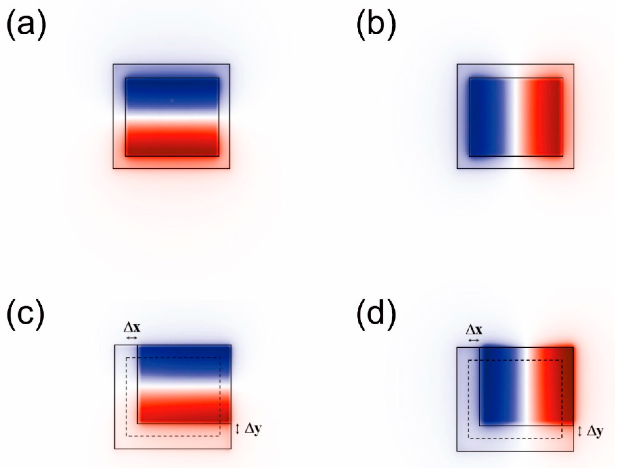
Figure 3.
(a) Lateral movement of a small upper nanoblock, indicated by Δx and Δy. A transparent grey box represents an original upper block with no movement. The resonant wavelengths of the (b) M1 and (c) M2 as functions of x- (black) and y- (red) displacements of the cavity with a fixed air gap size of 10 nm. Insets show the mode profiles of M1 and M2 in the cavity with no movement.

Figure 4.
(a) Absorption cross-section spectrum of the 2D plasmonic ruler without upper nanoblock movement, (Δx = 0 nm and Δy = 0 nm), denoted by (0-0). Two absorption peaks are observed at 882.2 nm (M1) and 1081.3 nm (M2). Absorption cross-section spectra with respect to Δx (nm) and Δy (nm) values of (b) 30 nm, 0 nm (30-0), (c) 0 nm, 30 nm (0-30), and (d) 30 nm, 30 nm (30-30). The black line indicates a reference absorption spectrum (0-0) and the red line indicates the absorption spectrum of the cavity with a moved upper block.

Figure 5.
2D color mapping of the absorption cross-section peak wavelengths of (a) mode 1 (M1) and (b) mode 2 (M2) as functions of Δx (nm) and Δy (nm). Cyan lines in (a) M1 and (b) M2 indicate resonant wavelengths—882.2 and 1081.3 nm—for the movement of Δx = 0 nm, Δy = 0 nm. Black lines indicate 885.1 and 1064.7 nm for the movement of Δx = 30 nm and Δy = 0 nm, respectively. The color bar at the right represents the absorption cross-section peak wavelengths.
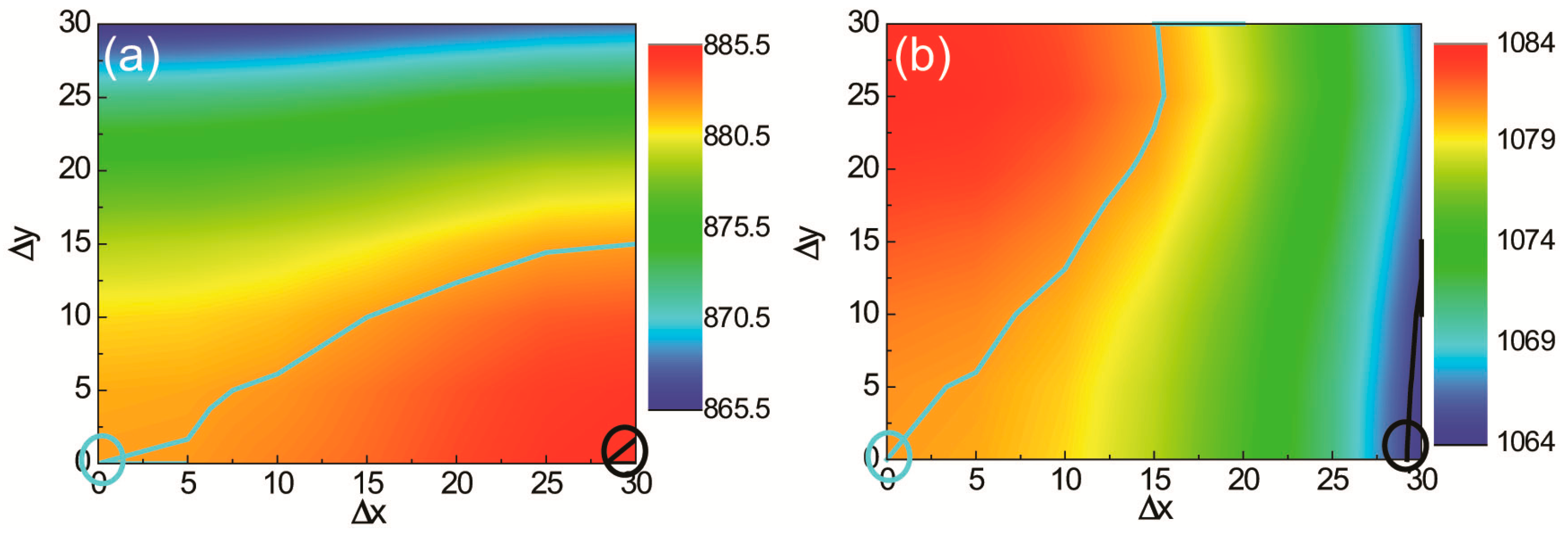
Figure 6.
(a) A schematic diagram of the vertical movement of the small upper block with a shift of Δz without a lateral movement. (b) Resonant wavelengths of mode 1 (M1) (black) and mode 2 (M2) (red) as functions of gap thickness.
Figure 6.
(a) A schematic diagram of the vertical movement of the small upper block with a shift of Δz without a lateral movement. (b) Resonant wavelengths of mode 1 (M1) (black) and mode 2 (M2) (red) as functions of gap thickness.
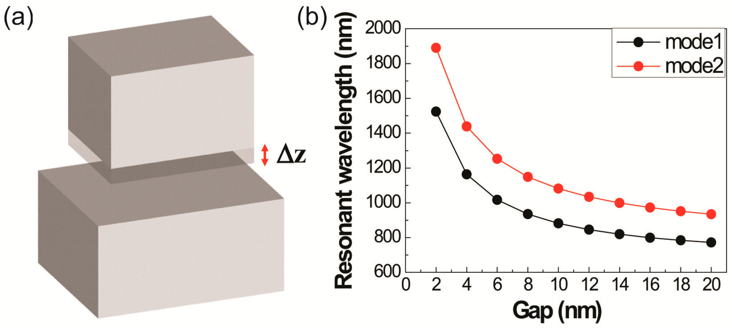
Figure 7.
(a) A schematic diagram of a 3D plasmonic ruler. A central larger block moves freely in 3D space with a movement of Δx (nm), Δy (nm), and Δz (nm). Upper and lower blocks have dimensions of 200 nm × 150 nm × 100 nm, and the central block has dimensions of 260 nm × 210 nm × 100 nm. Absorption cross-section spectra as functions of wavelength (b) without a movement of the central block, denoted by (0-0-0), and with a movement of the central block (c) only 2 nm along the z-direction (0-0-2) and (d) 30 and 2 nm along the x- and z-directions (30-0-2), respectively. P1 and P3 indicate the absorption peaks of mode 1 and mode 2, respectively, excited at the lower gap of 12 nm and P2 and P4 indicate the peaks of mode 1 and mode 2 at the upper gap of 8 nm.
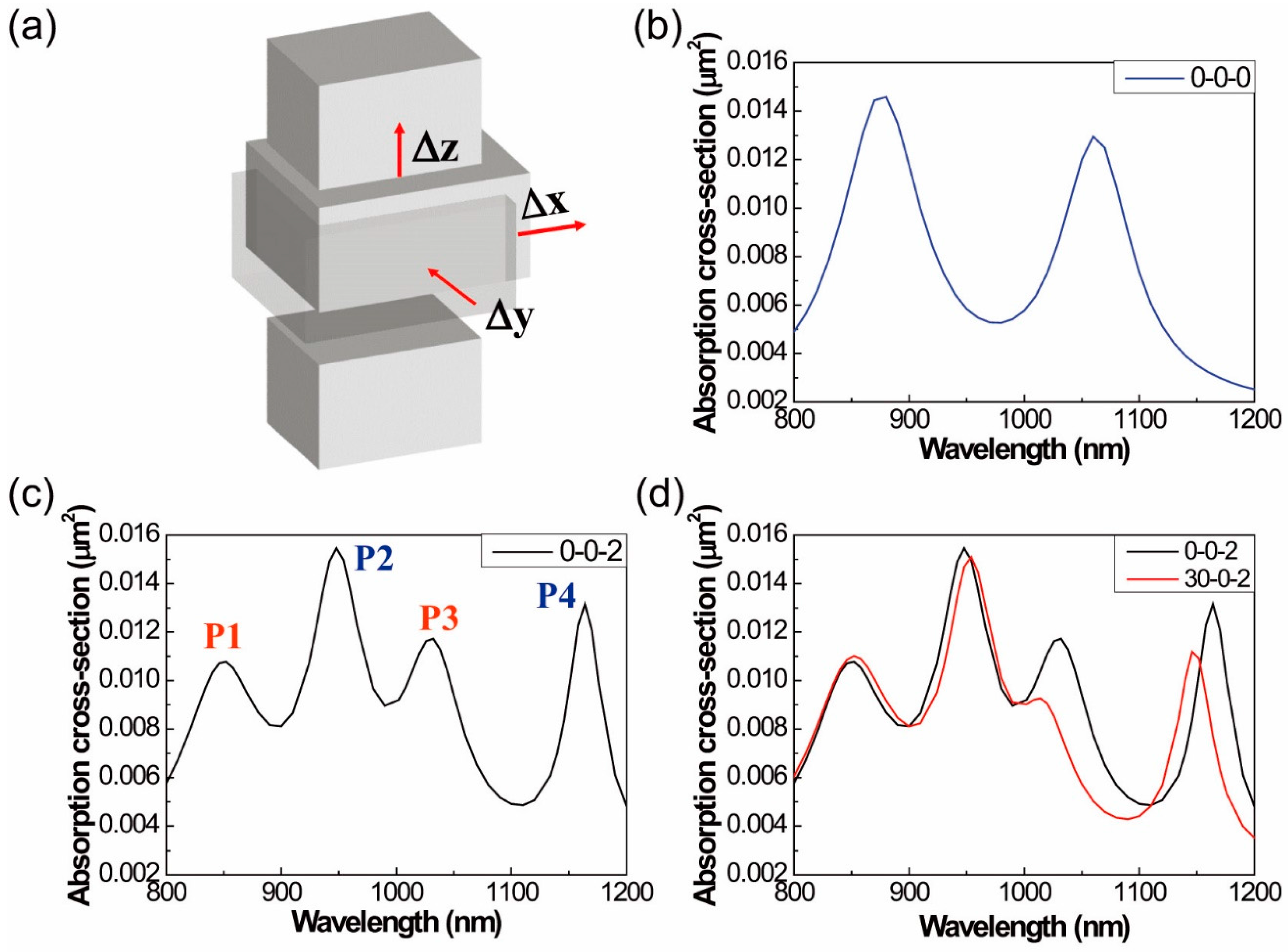
Figure 8.
(a) 3D surface mapping of absorption cross-section peak wavelengths of mode 1 and mode 2 for the upper air gap and the lower air gap for the movement of the central block, Δx = 30 nm, Δy = 0 nm, and Δz = 2 nm. The surfaces indicate the positions of the center block, where the absorption wavelength is maintained as constant. Mode 1 (P1, 852.1 nm) and mode 2 (P3, 1017.5 nm) for the lower gap of 12 nm are represented by red and cyan, respectively. Mode 1 (P2, 953.3 nm) and mode 2 (P4, 1148.3 nm) for the upper gap of 8 nm are indicated by yellow and blue, respectively. Red and blue lines represent the line of the intersection of the two surfaces, P2 and P4, P1 and P3, respectively, which are projected on an x–y plane. (b) The projection of the two red and blue lines on the x–y plane. The black circle indicates the cross-sectional point.
© 2018 by the authors. Licensee MDPI, Basel, Switzerland. This article is an open access article distributed under the terms and conditions of the Creative Commons Attribution (CC BY) license (http://creativecommons.org/licenses/by/4.0/).
Share and Cite
MDPI and ACS Style
Lee, T.-W.; Lee, Y.J.; Shin, E.; Kwon, S.-H. Nanometric Plasmonic Rulers Based on Orthogonal Plasmonic Gap Modes in Metal Nanoblocks. Appl. Sci. 2018, 8, 386. https://doi.org/10.3390/app8030386
AMA Style
Lee T-W, Lee YJ, Shin E, Kwon S-H. Nanometric Plasmonic Rulers Based on Orthogonal Plasmonic Gap Modes in Metal Nanoblocks. Applied Sciences. 2018; 8(3):386. https://doi.org/10.3390/app8030386
Chicago/Turabian StyleLee, Tae-Woo, Young Jin Lee, Eunso Shin, and Soon-Hong Kwon. 2018. "Nanometric Plasmonic Rulers Based on Orthogonal Plasmonic Gap Modes in Metal Nanoblocks" Applied Sciences 8, no. 3: 386. https://doi.org/10.3390/app8030386
Note that from the first issue of 2016, this journal uses article numbers instead of page numbers. See further details here.