Bloch Surface Waves Using Graphene Layers: An Approach toward In-Plane Photodetectors
by
 , , ,
, , ,
Richa Dubey
1,* ,
,
Miriam Marchena
2,
Babak Vosoughi Lahijani
1,
Myun-Sik Kim
1,
Valerio Pruneri
2,3 and
Hans Peter Herzig
1 1
Optics & Photonics Technology Laboratory (OPT), École Polytechnique Fédérale de Lausanne (EPFL), Rue de la Maladière 71b, 2002 Neuchâtel, Switzerland
2
Institut de Ciències Fotòniques (ICFO), The Barcelona Institute of Science and Technology, 08860 Castelldefels, Spain
3
Institució Catalana de Recerca i Estudis Avançats (ICREA), 08010 Barcelona, Spain
*
Author to whom correspondence should be addressed.
Appl. Sci. 2018, 8(3), 390; https://doi.org/10.3390/app8030390
Submission received: 9 February 2018
/
Revised: 2 March 2018
/
Accepted: 5 March 2018
/
Published: 7 March 2018
(This article belongs to the Special Issue Surface Waves on Planar Photonic Crystals)
Abstract
:A dielectric multilayer platform was investigated as a foundation for two-dimensional optics. In this paper, we present, to the best of our knowledge, the first experimental demonstration of absorption of Bloch surface waves in the presence of graphene layers. Graphene is initially grown on a Cu foil via Chemical Vapor Deposition and transferred layer by layer by a wet-transfer method using poly(methyl methacrylate), (PMMA). We exploit total internal reflection configuration and multi-heterodyne scanning near-field optical microscopy as a far-field coupling method and near-field characterization tool, respectively. The absorption is quantified in terms of propagation lengths of Bloch surface waves. A significant drop in the propagation length of the BSWs is observed in the presence of graphene layers. The propagation length of BSWs in bare multilayer is reduced to 17 times shorter in presence of graphene monolayer, and 23 times shorter for graphene bilayer.
1. Introduction
The electromagnetic surface waves propagating at the interface between dielectric multilayer platform and external medium are called Bloch Surface Waves (BSWs) [1,2]. A dielectric multilayer platform, sustaining BSWs, has been studied extensively for many applications, such as sensing and in-plane optics [3,4,5]. The modes propagating on the multilayer interface decay exponentially inside the multilayers due to the presence of the photonics band gap [1]. At the same time, modes are not allowed to propagate in the external medium, which is air in this study, because of total internal reflection. This salient propagation mechanism keeps the modes bound close to the multilayer surface. Absorption into the material, surface scattering, and leakage into the multilayer due to prism coupling are the main sources of the decay of the surface mode amplitude along the propagation direction [5,6,7]. The present design of the multilayer, whose details are provided in the ‘Materials and Methods’ section, is based on the optimized design for longer propagation lengths [8]. The BSW platform provides the possibility of ample choice of constituent material, provided that the material is transparent at the operating wavelengths. In addition, the maximum field amplitude of the BSW mode can be tuned at the surface of the dielectric multilayer [9,10]. This ability to tune the local field confinement is attractive for sensing applications [11,12].
The aforementioned advantages and features make the BSW platform an interesting candidate for the development of 2D optical systems [13,14,15]. To this end, several 2D optical components based on BSWs have been studied theoretically and experimentally. They include waveguides [16,17], lenses [5,18], disk resonators [19,20], BSW reflectors [21], Bessel-like beams [22,23,24,25], subwavelength focusers [26], phase-shifted Bragg gratings [27] and grating couplers [28,29]. Moreover, tunable planar optical components on BSW platforms have been demonstrated [30,31]. However, to envision BSW-based 2D integrated optical systems, detectors and light sources are inevitable elements to be studied. In this paper, we focus on in-plane detectors for BSW-based multilayer platforms, whereby the absorption mechanism of the surface waves is an important subject of study. To this end, we exploit the absorption properties of the graphene layer deposited on the top of the multilayer platform.
Graphene is a two-dimensional single layer of carbon atoms with sp2 hybridization forming a hexagonal lattice. Graphene exhibits exceptional electrical and optical properties. Thanks to its zero band gap semiconductor structure providing unique electronic properties, graphene has attracted much attention from researchers. Several high-speed electronic devices have already been proposed, thanks to the ultrafast response of the graphene [32]. Similarly to the electronic properties of graphene, its optical properties show an equal interest due to the strong interaction of graphene with light over a broadband range of wavelengths. The optical conductivity of graphene (from visible to infrared wavelengths) leads to an absorption of 2.3% of light in the case of a monolayer [33]. Indeed, graphene has become an attractive photonic material for a wide range of applications, such as photovoltaic devices, optical modulators and photodetectors, etc. [34]. Another significant advantage of graphene is the possibility of tuning its optical properties by applying external fields (electrical doping) or nonlinear optical effects [35]. With the advantage of tunable optical absorption and ultrafast response, graphene has become a promising candidate for on-chip integrated silicon photonics. For example, graphene-based photodetectors integrated on Si waveguides have been studied by S. Schuler et al. [34]. The spatial confinement and the propagation length of surface waves in the graphene layer has also been studied [36].
In this paper, the absorption of BSWs has been demonstrated experimentally for one and two layers of grapheme—monolayer and bilayer graphene, respectively—which act as absorption layers on top of the multilayer platform. Theoretically, the existence of BSWs on graphene-based multilayer platforms has been studied previously [33]. The thicknesses of monolayer and bilayer graphene are about 3 angstroms and 6 angstroms, respectively. The transference of the graphene layers from the initial Cu foil to the BSW platform is demonstrated in the subsequent section. A glass prism-based BSW excitation configuration is used to couple light to the graphene layers. Additionally, near-field measurements are performed using scanning near-field microscopy, which records evanescent fields of the surface waves to map the field distribution over graphene layers. Our study will pave the way to exploiting the electro-optic properties of graphene for detectors and other active components on BSW platforms.
2. Materials and Methods
The dielectric multilayer platform presented in this study consists of six periods of alternating high and low index layers. The low index and high index material layers are silicon dioxide (SiO2) and silicon nitride (SiNx) with refractive indexes of 1.45 and 1.79, respectively, around the wavelength λ = 1550 nm. The thicknesses of the SiNx and SiO2 layers are 283 nm and 472 nm, respectively. To terminate the precocity of the multilayers, a 50-nm-thick layer of SiNx is deposited on the top. This top layer is addressed as a defect layer. The complete stack (periodic multilayers + defect layer) is called the bare multilayer (BML) platform. The BML structure is deposited on a glass wafer, as shown in Figure 1. In the present study, multilayers are designed to support transverse electric (TE) polarization of incident light at telecommunication wavelengths. The multilayer platform is fabricated using the Plasma-Enhanced Chemical Vapor Deposition (PECVD, PlasmaLab 80+ by Oxford Instruments, Abingdon-on-Thames, UK) technique.
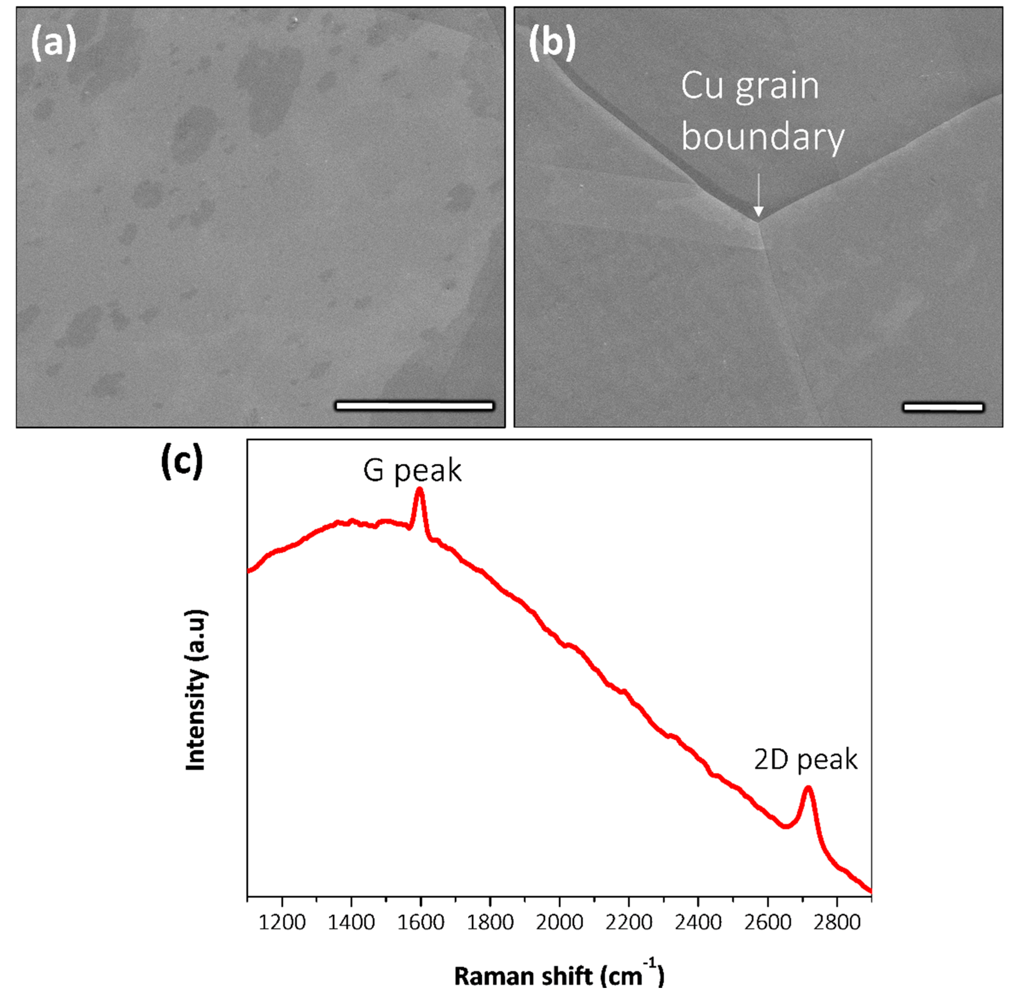
For graphene growth, we used a Cu foil of 25 µm thickness (Sigma Aldrich, Saint Louis, MO, USA) as a catalytic substrate on which monolayer graphene is deposited by Chemical Vapor Deposition (CVD, Black Magic 4-inch, AIXTRON, Herzogenrath, Germany) under the following conditions: CH4:H2 (1:4), 25 mbar and 10 min. Prior to the graphene growth, the cleaning and thermal treatment of the Cu foil is crucial for obtaining high quality graphene. The foil was cleaned by rinsing it in organic solvents and DI water (acetone:isopropyl alcohol:H2O, 2 min each), and finally in 0.1 M aqueous acetic acid (CH3COOH) for 2 min to remove the oxides formed on the Cu surface. After that, the Cu foil was immediately placed inside the CVD chamber to prevent oxidation, and it was heated at 50 °C min−1—from room temperature to 900 °C under an Ar/H2 flow for 15 min—performing an annealing step to improve the foil quality (grain size and crystallinity). Finally, the temperature was increased to 1000 °C, and the gases were fed into the chamber for graphene deposition. After cooling down the system, the graphene on the Cu foil is characterized by SEM, as shown in Figure 2a,b. In both images, a very clean and homogeneous graphene can be observed, whereby the presence of large Cu grain boundaries is highlighted in Figure 2b. Raman spectroscopy in Figure 2c has also been performed on the graphene on Cu foil, which detected the two typical peaks of graphene; G and 2D peaks, at 1580 cm−1 and 2680 cm−1, respectively. The absence of the D peak at 1350 cm−1—which is related to structural defects—confirms the growth of a high-quality graphene monolayer.
After growth, the graphene is transferred from the Cu foil to the BML platform. The procedure used is a wet-transfer method where poly (methyl methacrylate), (PMMA) is spin-coated on graphene/Cu at 4000 rpm. After drying it in air for 30 min, the whole structure is placed floating on a Cu etchant solution (0.05 g/mL, ammonium persulfate) for 4 h. The PMMA avoids the graphene collapse during the Cu etching. To avoid etchant residues, PMMA/graphene is rinsed three times in deionized (DI) water and placed on the BML platform. After drying the structure and storing it overnight in vacuum to remove H2O residues between graphene and the substrate, PMMA is removed by dipping the samples in acetone and isopropyl alcohol (15 min at each solvent). In order to build bilayer graphene structures on top of the BML platform, the PMMA transfer was repeated twice [37].
To couple incident light with the surface waves, we use the Kretschmann configuration [38]. The schematic of the experimental setup is shown in Figure 1, where a glass prism is required to fulfill the phase-matching condition to excite the BSWs. We illuminate the sample with a focused Gaussian beam to couple light with the BSW. At an incident angle ‘θ’, which is higher than the critical angle, the incident light is coupled with the BSW at a specific wavelength. We keep the BSW coupling zone approximately 30 µm away from the graphene layer. The phenomenon of BSW coupling can be seen as a reflection dip of the angular reflectance plot in the far-field (FF). We use CCD IR camera to collect the reflected light in the far-field on the other side of prism, see Figure 1. More details can be found in reference [8]. For BML, the BSWs can be coupled at an incident angle θ = 50.15°, at the corresponding wavelength λ = 1558 nm. The m-line pattern can be observed in the prism coupling configuration. These lines are defined as the order of the modes that can be excited in thin films at a specific angle [39]. The light of these propagating modes leaks out of the multilayer due to the presence of the prism. The interference of these leaky modes and total internally reflected incident light produces a specific fringe pattern, which can be observed in the far-field, see Figure 3a. The fringe pattern can also be understood as an interaction of total internally reflected incident beam and leaky propagating surface wave [40]. The reflected beam is a divergent Gaussian beam, while the leaky surface wave is more flat. The intersection of two wave-fronts having different curvatures produces the interference pattern. The absence of either of the two will cause the fringes to cease to exist. For example, fringes will not appear either in the case of non-diverging (flat waveforms) reflected light, or when there is no leaky propagating surface wave. In the present study, the latter is imposed by the absorption in the presence of the graphene layer.
In the case of BML+ graphene layers, the optimum condition of BSW coupling is found at the same angle of incidence as BML at the wavelength λ = 1558 nm. The thicknesses of the graphene layers (<1 nm) might be the reason behind the same coupling angle [33]. However, in the presence of graphene layers, only a broad dark band can be observed, as shown in Figure 3b. The dark band represents the significant absorption of propagating BSWs in the presence of graphene. The absorption reduces the propagation, and hence the leakage, of propagated BSWs. In consequence, we do not observe an interference fringe pattern in the far-field (see Figure 3b).
To perform the near-field measurements, we work with a multi-heterodyne scanning near-field optical microscope (MH-SNOM) in collection mode, which collects the evanescent electric field with a subwavelength aperture fiber probe. Because BSWs propagate at the interface of multilayers, near-field microscopy is an optimum tool for performing the spatial field distribution mapping locally. Further details about MH-SNOM can be found elsewhere [10].
3. Results and Discussion
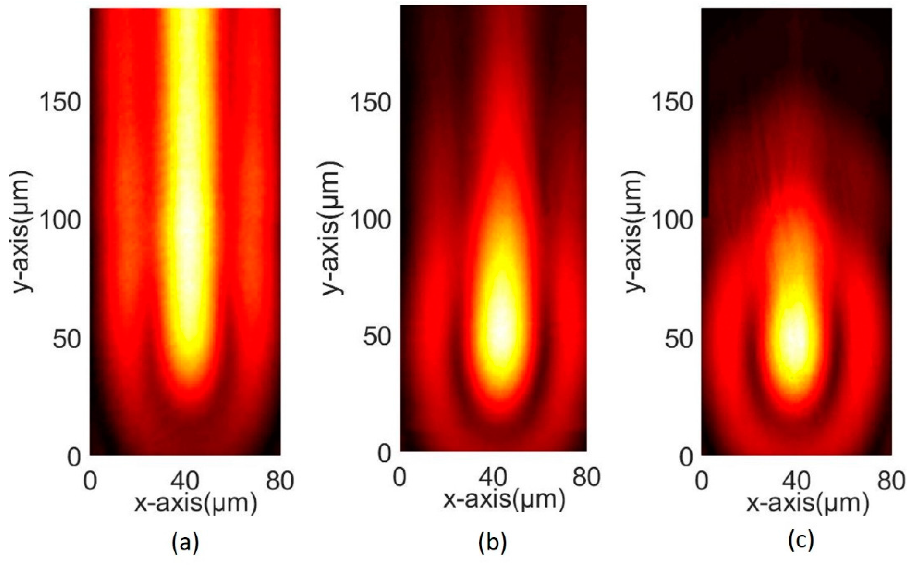
The light is coupled evanescently to the graphene layer using a Kretschmann configuration. Further, with the aid of MH-SNOM, propagation lengths of BSWs (LBSW) for BML, monolayer graphene and bilayer graphene are measured in the near-field, as shown in Figure 4. For the comparison of absorption of the propagating field, we show here the propagation of BSW without any graphene layer/bare multilayer (Figure 4a), with monolayer graphene (Figure 4b) and with bilayer graphene (Figure 4c).
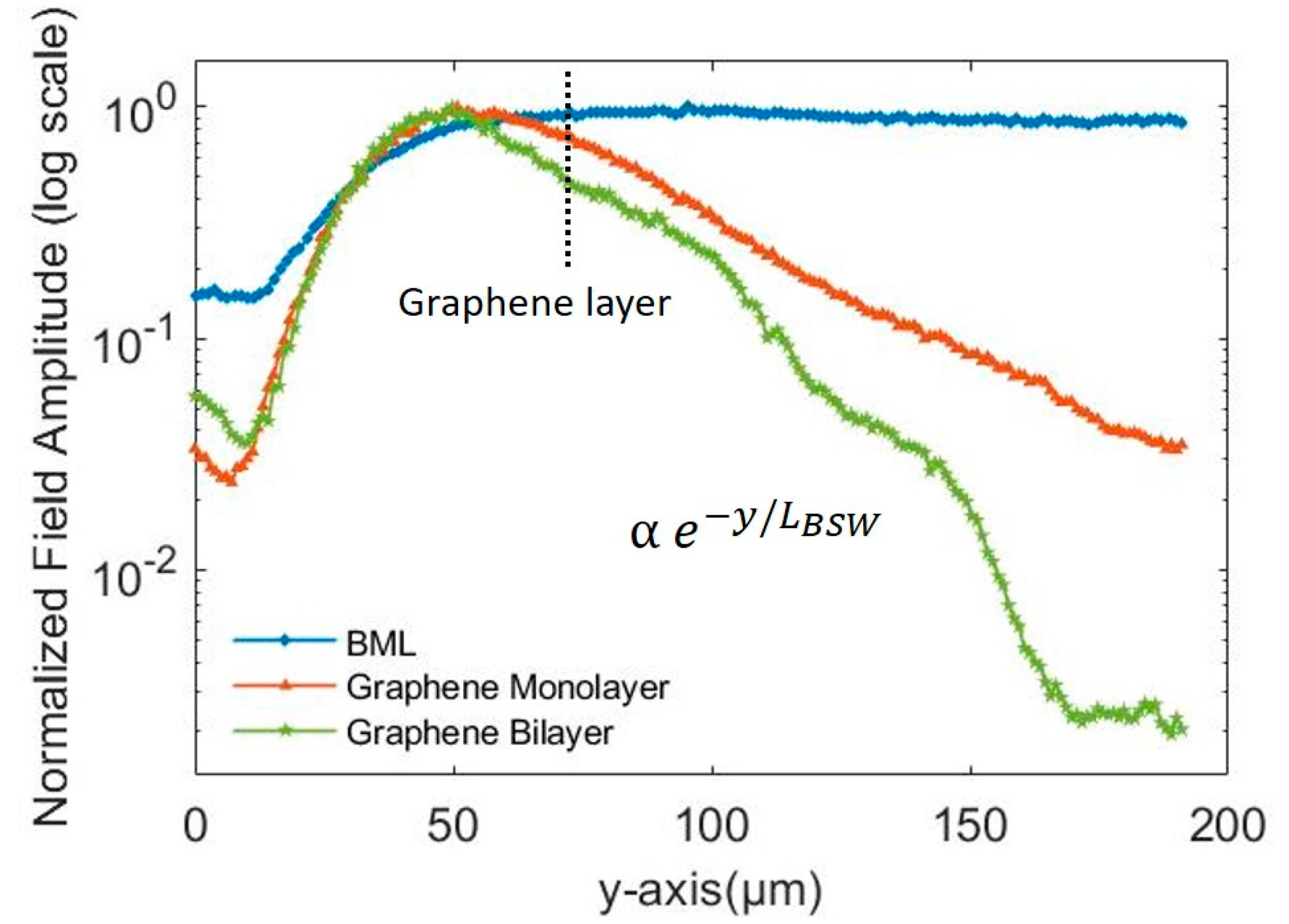
The propagation lengths are defined as the distance at which the amplitude of the propagating field drops to 1/e of its maximum value. The LBSWS are deduced by exponentially fitting the decay of the measured field amplitude of the surface wave along the propagation direction [10]. Figure 5 shows the logarithmic scale of the cross-section of the exponentially decaying field amplitude profiles of the BML, monolayer and bilayer graphene, respectively. The measured LBSW for BML when using monolayer and bilayer graphene are approximately 1300 µm [8], 75 µm and 55 µm, respectively. From the measurement results, we observe that the propagation lengths in graphene layers are reduced drastically in comparison to BML; roughly 17 times shorter for the monolayer and 23 times shorter for the bilayer of graphene. This is due to strong absorption resulting from the presence of graphene layers along the direction of propagation. The reason behind the smaller influence of the graphene bilayer on absorption than the monolayer is the difference in the level of doping between both cases. The intrinsic absorption properties of graphene depend on the level of doping. In the case of monolayer, the graphene is sitting on the substrate and has air on the other side. The first layer of the bilayer graphene has graphene on the other side, unlike the monolayer. While the second layer of the bilayer graphene has graphene on one side and air on other side. These boundary conditions can justify a different doping [41].
The propagation length of leaky modes in a prism coupling system can also be deduced from the angular width of reflection anomaly in far-field [8]. The propagation lengths vary in a fashion inversely proportional to the width of the reflection spectrum. More details of the method can be found in ref. [8].
Thanks to the atomic layer thicknesses of graphene layers (3 angstroms and 6 angstrom for the monolayer and bilayer, respectively), graphene does not require an additional propagation constant other than the bare multilayer, and hence the coupling condition. Therefore, surface waves are directly absorbed by graphene layers without the necessity of external coupling devices, unlike silicon photonics. In a study of integrated GaInAsSb photodiode on silicon waveguide, the diffraction gratings are employed as an external coupling device to interface the silicon waveguide with the photodiode [42]. The poor coupling efficiency of the grating coupler is stated as the main reason behind the degraded performance of the detector [42].
In addition, the CVD graphene growth and its transfer to the multilayer platform by the wet-transfer method using PMMA provides an easier fabrication (integration) process in comparison to conventional silicon photonics integration processes.
4. Conclusions
The absorption properties of monolayer and bilayer graphene on a BSW platform have been studied using near-field optical microscopy technique. To the best of our knowledge, this is the first experimental demonstration of graphene-induced absorption of BSW propagation. The propagation lengths of BSWs for BML and BML+ graphene layers have been compared. The results show that propagation length in the presence of monolayer and bilayer graphene is decreased significantly (approximately 17 times and 23 times shorter, respectively) than the bare multilayer. This is due to the strong absorption of the graphene layer. This study provides an advancement in the direction of the development of BSW-based 2D integrated optical systems, in particular in-plane photodetectors.
Acknowledgments
We acknowledge funding from Swiss National Science Foundation (SNSF) (200020_135455), from the Spanish Ministry of Economy and Competitiveness through the “Severo Ochoa” Programme for Centres of Excellence in R&D (SEV-2015-0522) and OPTO-SCREEN (TEC2016-75080-R), from the European Union H2020 Programme under grant agreement No. 696656 “Graphene Flagship”, from Fundació Privada Cellex, and from Generalitat de Catalunya through the CERCA program.
Author Contributions
R.D. performed near-field experiments, far-field experiments, data analysis and wrote the manuscript. M.M. performed the deposition of graphene layers on the top of multilayer platform and wrote the fabrication details. B.V.L. contributed to the interpretation of results and preparation of the manuscript. M.-S.K. supported the scientific discussions of the results. V.P. supervised the work at Barcelona Institute of Science and Technology. H.P.H. supervised and guided the work at École Polytechnique Fédérale de Lausanne. The final manuscript is the result of common contributions and discussions. All the authors read and approved the final manuscript.
Conflicts of Interest
The authors declare that they have no competing interests.
References
- Yeh, P.; Yariv, A.; Cho, A.Y. Optical surface waves in periodic layered media. Appl. Phys. Lett. 1978, 32, 104–105. [Google Scholar] [CrossRef]
- Liscidini, M.; Sipe, J.E. Enhancement of diffraction for biosensing applications via Bloch surface waves. Appl. Phys. Lett. 2007, 91, 253125. [Google Scholar] [CrossRef]
- Descrovi, E.; Frascella, F.; Sciacca, B.; Geobaldo, F.; Dominici, L.; Michelotti, F. Coupling of surface waves in highly defined one-dimensional porous silicon photonic crystals for gas sensing applications. Appl. Phys. Lett. 2007, 91, 241109. [Google Scholar] [CrossRef]
- Giorgis, F.; Descrovi, E.; Summonte, C.; Dominici, L.; Michelotti, F. Experimental determination of the sensitivity of Bloch surface waves based sensors. Opt. Express 2010, 18, 8087–8093. [Google Scholar] [CrossRef] [PubMed]
- Yu, L.; Barakat, E.; Sfez, T.; Hvozdara, L.; Di Francesco, J.; Herzig, H.P. Manipulating Bloch surface waves in 2D: A platform concept-based flat lens. Light Sci. Appl. 2014, 3, 124. [Google Scholar] [CrossRef]
- Soboleva, I.V.; Descrovi, E.; Summonte, C.; Fedyanin, A.A.; Giorgis, F. Fluorescence emission enhanced by surface electromagnetic waves on one-dimensional photonic crystals. Appl. Phys. Lett. 2009, 94, 231122. [Google Scholar] [CrossRef]
- Ulrich, R. Theory of the prism-film coupler by plane-wave analysis. J. Opt. Soc. Am. 1970, 60, 1337–1350. [Google Scholar] [CrossRef]
- Dubey, R.; Barakat, E.; Häyrinen, M.; Roussey, M.; Honkanen, S.; Kuittinen, M.; Herzig, H.P. Experimental investigation of the propagation properties of Bloch surface waves on dielectric multilayer platform. J. Eur. Opt. Soc. 2017, 13, 1–9. [Google Scholar] [CrossRef]
- Khan, M.U.; Corbett, B. Bloch surface wave structures for high sensitivity detection and compact waveguiding. Sci. Technol. Adv. Mater. 2016, 17, 398–409. [Google Scholar] [CrossRef] [PubMed]
- Dubey, R. Near-Field Characterization of Bloch Surface Waves Based 2D Optical Components. Ph.D. Thesis, École Polytechnique Fédérale de Lausanne, Lausanne, Switzerland, 2017. [Google Scholar]
- Konopsky, V.N.; Alieva, E.V. Photonic crystal surface waves for optical biosensors. Anal. Chem. 2007, 79, 4729–4735. [Google Scholar] [CrossRef] [PubMed]
- Robertson, W.M. Experimental measurement of the effect of termination on surface electromagnetic waves in one-dimensional photonic bandgap arrays. J. Light. Technol. 1999, 17, 2013–2017. [Google Scholar] [CrossRef]
- Herzig, H.P.; Barakat, E.; Dubey, R.; Kim, M.-S. Optics in 2D Bloch surface wave phenomena and applications. In Proceedings of the 15th Workshop on Information Optics (WIO), Barcelona, Spain, 11–15 July 2016. [Google Scholar] [CrossRef]
- Dubey, R.; Barakat, E.; Herzig, H.P. Bloch surface waves based platform for integrated optics. In Proceedings of the IEEE Photonics Conference, Reston, VA, USA, 4–8 October 2015. [Google Scholar] [CrossRef]
- Herzig, H.P.; Barakat, E.; Yu, L.; Dubey, R. Bloch surface waves, a 2D platform for planar optical integration. In Proceedings of the 13th Workshop on Information Optics (WIO), Neuchatel, Switzerland, 7–11 July 2014. [Google Scholar] [CrossRef]
- Sfez, T.; Descrovi, E.; Yu, L.; Quaglio, M.; Dominici, L.; Nakagawa, W.; Michelotti, F.; Giorgis, F.; Herzig, H.P. Two-dimensional optics on silicon nitride multilayer: Refraction of Bloch surface waves. Appl. Phys. Lett. 2010, 96, 151101. [Google Scholar] [CrossRef]
- Sfez, T.; Descrovi, E.; Yu, L.; Brunazzo, D.; Quaglio, M.; Dominici, L.; Herzig, H.P. Bloch surface waves in ultrathin waveguides: Near-field investigation of mode polarization and propagation. J. Opt. Soc. Am. A 2010, 27, 1617–1625. [Google Scholar] [CrossRef]
- Angelini, A.; Lamberti, A.; Ricciardi, S.; Frascella, F.; Munzert, P.; Leo, N.D.; Descrovi, E. In-plane 2D focusing of surface waves by ultrathin refractive structures. Opt. Lett. 2014, 39, 6391–6394. [Google Scholar] [CrossRef] [PubMed]
- Dubey, R.; Lahijani, B.V.; Barakat, E.; Häyrinen, M.; Roussey, M.; Kuittinen, M.; Herzig, H.P. Near-field characterization of a Bloch-surfacewave-based 2D disk Resonator. Opt. Lett. 2016, 41, 4867–4870. [Google Scholar] [CrossRef] [PubMed]
- Lahijani, B.V.; Ghavifekr, H.B.; Dubey, R.; Kim, M.-S.; Vartiainen, I.; Roussey, M.; Herzig, H.P. Experimental demonstration of critical coupling of whispering gallery mode cavities on Bloch surface wave platform. Opt. Lett. 2017, 42, 5137–5140. [Google Scholar] [CrossRef] [PubMed]
- Dubey, R.; Lahijani, B.V.; Häyrinen, M.; Roussey, M.; Kuittinen, M.; Herzig, H.P. Ultra-thin Bloch surface waves based reflector at telecommunication wavelength. Photonics Res. 2017, 5, 494–499. [Google Scholar] [CrossRef]
- Kim, M.-S.; Dubey, R.; Barakat, E.; Herzig, H.P. Nano-thin 2D axicon generating nondiffracting surface waves. In Proceedings of the Optical MEMS and Nanophotonics (OMN), Singapore, 31 July–4 August 2016. [Google Scholar] [CrossRef]
- Kim, M.-S.; Barakat, E.; Dubey, R.; Scharf, T.; Herzig, H.P. Nondiffracting Bloch surface wave: 2D quasi-Bessel-Gauss beam. In Proceedings of the OSA CLEO Pacific Rim Conference, Busan, Korea, 24–28 August 2015. [Google Scholar] [CrossRef]
- Dubey, R.; Lahijani, B.V.; Kim, M.-S.; Barakat, E.; Häyrinen, M.; Roussey, M.; Kuittinen, M.; Herzig, H.P. Near-field investigation of Bloch surface wave based 2D optical components. In Proceedings of the SPIE Photonics West 10106, San Francisco, CA, USA, 16 February 2017. [Google Scholar] [CrossRef]
- Wang, R.; Wang, Y.; Zhang, D.; Si, G.; Zhu, L.; Du, L.; Kou, S.; Badugu, R.; Rosenfeld, M.; Lin, J.; et al. Diffraction-Free Bloch Surface Waves. ACS Nano 2017, 11, 5383–5390. [Google Scholar] [CrossRef] [PubMed]
- Kim, M.-S.; Lahijani, B.V.; Descharmes, N.; Straubel, J.; Negredo, F.; Rockstuhl, C.; Häyrinen, M.; Roussey, M.; Kuittinen, M.; Herzig, H.P. Subwavelength focusing of Bloch surface waves. ACS Photonics 2017, 4, 1477–1483. [Google Scholar] [CrossRef]
- Doskolovich, L.L.; Bezus, E.A.; Bykov, D.A.; Soifer, V.A. Spatial differentiation of Bloch surface wave beams using an on-chip phase-shifted Bragg grating. J. Opt. 2016, 18, 115006. [Google Scholar] [CrossRef]
- Kovalevich, T.; Boyer, P.; Suarez, M.; Salut, R.; Kim, M.S.; Herzig, H.P.; Bernal, M.P.; Grosjean, T. Polarization controlled directional propagation of Bloch surface wave. Opt. Express 2017, 25, 5710–5715. [Google Scholar] [CrossRef] [PubMed]
- Angelini, A.; Barakat, E.; Munzert, P.; Boarino, L.; De Leo, N.; Enrico, E.; Giorgis, F.; Herzig, H.P.; Pirri, C.F.; Descrovi, E. Focusing and extraction of light mediated by Bloch surface waves. Sci. Rep. 2014, 4, 5428. [Google Scholar] [CrossRef] [PubMed]
- Kovalevich, T.; Ndao, A.; Suarez, M.; Tumenas, S.; Balevicius, Z.; Ramanavicius, A.; Baleviciute, I.; Häyrinen, M.; Roussey, M.; Kuittinen, M.; et al. Tunable Bloch surface waves in anisotropic photonic crystals based on lithium niobate thin films. Opt. Lett. 2016, 41, 5616–5619. [Google Scholar] [CrossRef] [PubMed]
- Kovalevich, T.; Kim, M.S.; Belharet, D.; Robert, L.; Herzig, H.P.; Grosjean, T.; Bernal, M.P. Experimental evidence of Bloch surface waves on photonic crystals with thin film LiNbO3 as a top layer. Photonics Res. 2017, 5, 649–653. [Google Scholar] [CrossRef]
- Liang, G.; Neophytou, N.; Nikonov, D.E.; Lundstrom, M.S. Performance projections for ballistic graphene nanoribbon field-effect transistors. IEEE Trans. Electron. Devices 2007, 54, 677–682. [Google Scholar] [CrossRef]
- Sreekanth, K.V.; Zeng, S.; Shang, J.; Yong, K.-T.; Yu, T. Excitation of surface electromagnetic waves in a graphene-based Bragg grating. Sci. Rep. 2012, 2, 737. [Google Scholar] [CrossRef] [PubMed]
- Schuler, S.; Schall, D.; Neumaier, D.; Dobusch, L.; Bethge, O.; Schwarz, B.; Krall, M.; Mueller, T. Controlled Generation of a p-n Junction in a Waveguide Integrated Graphene Photodetector. Nano Lett. 2016, 16, 7107–7112. [Google Scholar] [CrossRef] [PubMed]
- Zhou, Y.; Wang, C.; Xu, D.-H.; Fan, R.-H.; Zhang, K.; Peng, R.-W.; Hu, Q.; Wang, M. Tuning the dispersion relation of a plasmonic waveguide via graphene contact. Europhys. Lett. 2014, 107, 34007. [Google Scholar] [CrossRef]
- Merano, M. Transverse electric surface mode in atomically thin Boron–Nitride. Opt. Lett. 2016, 41, 2668–2671. [Google Scholar] [CrossRef] [PubMed]
- Marchena, M.; Janner, D.; Chen, T.L.; Finazzi, V.; Pruneri, V. Low temperature direct growth of graphene patterns on flexible glass substrates catalysed by a sacrificial ultrathin Ni film. Opt. Mater. Express 2016, 6, 2487–2507. [Google Scholar] [CrossRef]
- Kretschmann, E.; Raether, H. Radiative decay of nonradiative surface plasmons excited by light. Z. Naturforsch. 1968, 23, 2135–2136. [Google Scholar] [CrossRef]
- Tien, P.K.; Ulrich, R.; Martin, R.J. Modes of propagating light waves in thin deposited semiconductor films. Appl. Phys. Lett. 1969, 14, 291–294. [Google Scholar] [CrossRef]
- Konopsky, V.N.; Alieva, E.V. Observation of fine interference structures at total internal reflection of focused light beams. Phys. Rev. A 2012, 86, 063807. [Google Scholar] [CrossRef]
- Rodrigo, D.; Tittl, A.; Limaj, O.; de Abajo, F.J.G.; Pruneri, V.; Altug, H. Double-layer graphene for enhanced tunable infrared plasmonics. Light Sci. Appl. 2017, 6, 16277. [Google Scholar] [CrossRef]
- Gassenq, A.; Hattasan, N.; Cerutti, L.; Rodriguez, J.B.; Tournié, E.; Roelkens, G. Study of evanescently-coupled and grating assisted GaInAsSb photodiodes integrated on a silicon photonic chip. Opt. Express 2012, 20, 11665–11672. [Google Scholar] [CrossRef] [PubMed]
Figure 1.
Illustration of the Kretschmann configuration setup for BSW coupling with dielectric multilayers deposited on a glass wafer. The SNOM probe collects the evanescent field on top of the 2D structures. On the other side of the prism, there is a CCD camera to collect the light reflected in the far-field.

Figure 2.
(a,b) SEM characterization of continuous and clean graphene grown on a Cu foil. The arrows in (b) indicate the presence of the Cu grain boundaries; (c) Raman spectroscopy performed on graphene on Cu foil, showing the two typical peaks of graphene; G and 2D at 1580 and 2680 cm−1, respectively. The absence of the defect-related D peak at 1350 cm−1 confirms the growth of high-quality graphene. Scale bar: 5 µm.

Figure 3.
M-line pattern observed in the far-field image of the reflected light captured with a CCD camera in Kretschmann coupling configuration for (a) Bare multilayer; (b) Monolayer graphene.
Figure 3.
M-line pattern observed in the far-field image of the reflected light captured with a CCD camera in Kretschmann coupling configuration for (a) Bare multilayer; (b) Monolayer graphene.

Figure 4.
Near-field amplitude distribution acquired by MH-SNOM demonstrating BSW propagation for (a) Bare multilayer; (b) Monolayer graphene; and (c) Bilayer graphene.
Figure 4.
Near-field amplitude distribution acquired by MH-SNOM demonstrating BSW propagation for (a) Bare multilayer; (b) Monolayer graphene; and (c) Bilayer graphene.

Figure 5.
The normalized field amplitude cross section (in logarithmic scale) along the direction of propagation of BML, monolayer and bilayer of graphene.
Figure 5.
The normalized field amplitude cross section (in logarithmic scale) along the direction of propagation of BML, monolayer and bilayer of graphene.
© 2018 by the authors. Licensee MDPI, Basel, Switzerland. This article is an open access article distributed under the terms and conditions of the Creative Commons Attribution (CC BY) license (http://creativecommons.org/licenses/by/4.0/).
Share and Cite
MDPI and ACS Style
Dubey, R.; Marchena, M.; Vosoughi Lahijani, B.; Kim, M.-S.; Pruneri, V.; Herzig, H.P. Bloch Surface Waves Using Graphene Layers: An Approach toward In-Plane Photodetectors. Appl. Sci. 2018, 8, 390. https://doi.org/10.3390/app8030390
AMA Style
Dubey R, Marchena M, Vosoughi Lahijani B, Kim M-S, Pruneri V, Herzig HP. Bloch Surface Waves Using Graphene Layers: An Approach toward In-Plane Photodetectors. Applied Sciences. 2018; 8(3):390. https://doi.org/10.3390/app8030390
Chicago/Turabian StyleDubey, Richa, Miriam Marchena, Babak Vosoughi Lahijani, Myun-Sik Kim, Valerio Pruneri, and Hans Peter Herzig. 2018. "Bloch Surface Waves Using Graphene Layers: An Approach toward In-Plane Photodetectors" Applied Sciences 8, no. 3: 390. https://doi.org/10.3390/app8030390
Note that from the first issue of 2016, this journal uses article numbers instead of page numbers. See further details here.