Capacitive Power Transfer System with Reduced Voltage Stress and Sensitivity


1
ASEM, Interdisciplinary Graduate School of Engineering Sciences, Kyushu University, Fukuoka 816-8580, Japan
2
Department of Electrical and Computer Engineering, The University of Auckland, Auckland 1023, New Zealand
*
Author to whom correspondence should be addressed.
Appl. Sci. 2018, 8(7), 1131; https://doi.org/10.3390/app8071131
Submission received: 13 June 2018
/
Revised: 30 June 2018
/
Accepted: 9 July 2018
/
Published: 12 July 2018
(This article belongs to the Special Issue Wireless Power Transfer for Smart Industrial, Biomedical and Home Applications)
Abstract
:Featured Application
In this paper, we introduce a wireless power transfer system based on electric field coupling (capacitive coupling) with less voltage across the coupling interface and circuit quality factor by using a DC–DC converter, which resulted in a safer and less sensitive system while maintaining sufficient delivered power and high efficiency. The introduced system has a wide application range with different power needs and transmission distances, such as charging mobile devices including mobile phones, pads, laptops, drones, cameras, and wireless sensors. The system use can also be extended to supplying power to robots, smart walls, screens, lighting, indicative signs, and oil and gas applications.
Abstract
This paper introduces a DC–DC buck converter on the secondary side of the capacitive power transfer system to reduce the voltage and electric field across the interface, and to reduce the circuit Q, and thus the system sensitivity. The system is mathematically analyzed to study the improvement in sensitivity and voltage stress. The leakage electric field emissions around the plates are investigated by simulation. The analytical and simulation results show that by reducing the duty cycle of the buck converter at a constant output power, the voltage across the plates can be significantly reduced and the circuit becomes less sensitive to the variations in parameters. Experimental results demonstrated that Q and the voltage stress over the capacitive interface are reduced by changing the duty cycle of the buck converter. For delivering 10 W of power, the maximum voltage stress across one pair of the coupling plates is reduced from 211 V in the conventional system without using a DC–DC converter, to 65 V and 44 V at duty cycles of 30% and 20%, respectively. The system achieves an end-to-end power efficiency of 80% at an output power of 10 W and a duty cycle of 30%.
1. Introduction
Since the 1890s, efforts have focused on the wireless transfer of power [1], and the most successful approach has been inductive power transfer (IPT), which is based on magnetic field coupling. Inductive power transfer has been widely used for powering industrial machines [2,3], charging mobile devices [2,4] and electric vehicles [5,6], and powering biomedical implants [7]. However, IPT has clear limitations with regard to high eddy current losses to the surroundings especially with metals, high standing losses, and complicated design, requiring bulky and expensive magnetic materials and electromagnetic interference (EMI) shielding [8,9]. Also, given its nature, IPT is unable to transfer power across metal barriers. Capacitive power transfer (CPT), a technology that uses a varying electric field to transfer power, has been introduced as a good alternative to IPT for near field power transfer due to its unique features, such as design flexibility of coupling structure, ability to transfer power across electrically isolated metal barriers, low standing losses and EMI, and low cost and weight [10,11,12,13,14]. Capacitive power transfer can be used in various applications, such as integrated circuits (IC) [15], biomedical devices [16], consumer electronics [11,12,17,18,19], and electric vehicles (EVs) [20].
The conventional CPT system is illustrated in Figure 1, where the capacitive interface is typically in the range of hundreds of picofarads (pF) when the plates are almost touching with an insulation layer in between and 1–2 mm air gap, and few tens of picofarads when there is a wide air gap, e.g., 150 mm to 300 mm air gap is usually considered for EV charging applications [21]. This results in a high-quality factor and voltage stress across the capacitive interface. For example, if the operating frequency f is 1 MHz, the load resistance RL is 12.3 Ω, the capacitive interface Cc1 = Cc2 = 2Cc = 1 nF and the tuning inductor L is 50.7 μH, which provides the quality factor [22] Qconv of 8/π2RL (sqrt(L/Cc)) ≅ 32 and provides the maximum voltage stress across the single pair of the capacitive interface Vc_conv of 320 V for an AC input voltage Vin_conv of just 20 V. Consequently, practically attaining tuning is challenging, and the system is highly sensitive to coupling variation and load change. The high voltage stress across the coupling interface increases the probability of dielectric breakdown and sparks occurrence. In addition, system safety becomes an issue as the related leakage electric field emissions around the plates increase beyond the safety margins as will be detailed in Section 4. These matters result in lower efficiency, decreased ability to deliver power, and increased difficulty in offering commercially accepted systems.
Previous studies introduced a partial solution for the previously mentioned issues [10,21,23,24,25]; however, no comprehensive design overcomes both issues simultaneously. For instance, one pulse switching active capacitor (OPSAC) was proposed to overcome the sensitivity issue [24]; however, the system is complicated and the voltage stress across the coupling interface is high. Tuning the operating frequency [25] is an effective method to mitigate the sensitivity issue and even with a high-quality factor, the system can still transfer the power with high efficiency, but by changing the frequency, following the regulations becomes challenging and the design is complex, costly, and cannot avoid the high voltage stress.
In this paper, a CPT system with a DC–DC buck converter on the secondary side is introduced to simultaneously reduce the system sensitivity and the voltage stress across the capacitive interface. The proposed system can also keep the leakage electric field low, which improves the safety of CPT systems.
The rest of the paper is arranged as follows. Section 2 describes the structure of the proposed CPT system. The mathematical model and analysis are covered in Section 3. In Section 4, the leakage electric field simulation is outlined. A prototype is implemented for evaluation in Section 5. The conclusions are drawn in Section 6.
2. Proposed System Structure
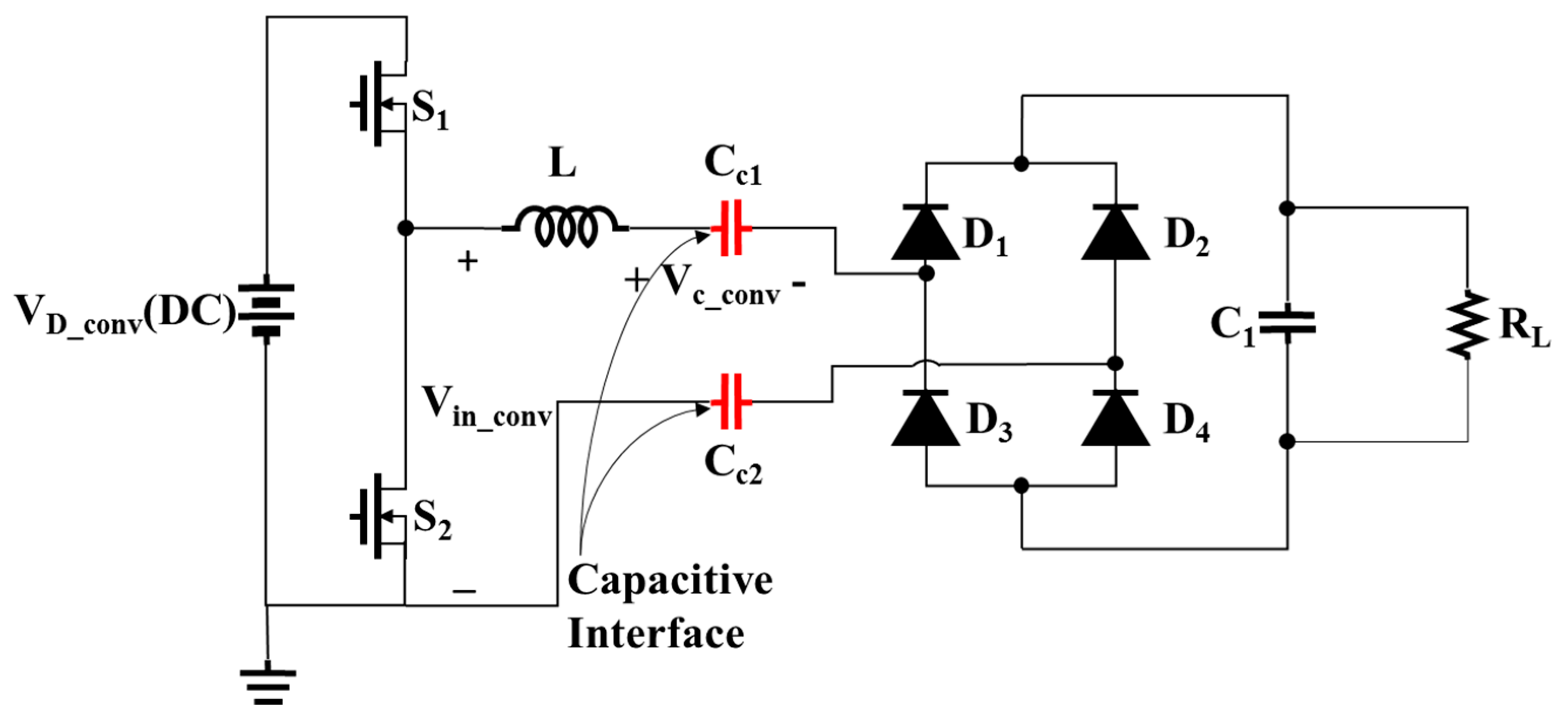
The structure of the proposed CPT system is shown in Figure 2a. Switches (S1–S2) construct a half-bridge inverter (full bridge can be used) to convert DC input voltage () into an AC signal. Inductor L is placed in series to compensate for the capacitive interface, where and represent the capacitive coupling interface. Diodes (D1–D4) construct the full wave rectifier to obtain DC voltage. The DC–DC buck converter supplies the voltage and current to the load.
3. Mathematical Modelling and Analysis
For analysis, the system topology of Figure 2a was rearranged assuming the parasitic resistances are neglected for all components, as shown in Figure 2c. The inverter in Figure 2a produces a square wave voltage. This voltage is applied to the input terminal of the resonant circuit. The resonant circuit frequency is tuned to the fundamental component of the inverter square wave, i.e., to the switching frequency f. As a result, the resonant circuit current and the resonant circuit output voltage and current have essentially sinusoidal waveforms at the fundamental frequency f, with negligible harmonics. Accordingly, the sinusoidal approximation was first considered where Vin can be obtained from Equation (1), as shown in Figure 2b.
The two series interface capacitances were replaced by Cc as shown in Equation (2). The series compensation inductor L is obtained from Equation (3). The equivalent AC load R [26], assuming the rectifier and the buck converter are ideal, is described in Equation (4).
where is the angular switching frequency; Rload is the effective load resistance at the AC side; which is equal to 81% of the actual load resistance RL at the DC side after the rectifier; and is the buck converter duty cycle. The values in Table 1 were used as a design example to prove the concept.
The equivalent circuit shown in Figure 2c would not be applicable for analysis if the cross coupling or the leakage capacitance is too high due to the complicated coupling configuration [27] or if the operating frequency is increased to a very high level. In these cases, more accurate modelling [14] for the capacitive interface should be used.
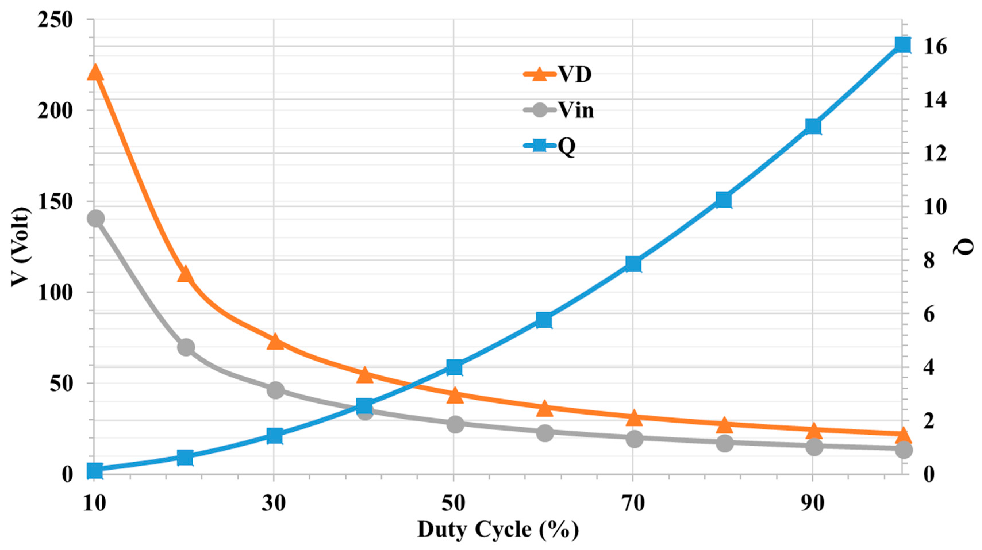
To fairly compare the system sensitivity and the voltage stress over the capacitive coupling interface in the proposed system and the conventional system previously described, we assumed that the same amount of power was delivered to the load and the input voltage would change according to the value of the duty cycle (D) of the buck converter. When D was 100% represented the conventional system. Figure 3 shows the needed input voltage for the design example to deliver 10 W to the load depending on D, as shown in Equations (5) and (6):
From Equation (1), we obtain:
where VD and Vin are the DC input voltage and AC input voltage needed to deliver a specific amount of power to the load, respectively. The DC input voltage and AC input voltage for the conventional system are represented by VD_conv and Vin_conv, respectively.
3.1. System Sensitivity
Figure 4 illustrates the frequency response of the output power with different duty cycles. The instantaneous real power transferred to the load is provided in Equation (7) and the average power in Equation (8). By reducing D, the output will have a wider response that is reflected in lower sensitivity. The quality factor of the proposed system (Q) as expressed in Equation (9) decreases proportionally to D2, as shown in Figure 3. By lowering Q, the sensitivity decreases and tuning at resonant frequency will be more obtainable practically. For a less sensitive system, we recommend using , which can be easily achieved by choosing for the chosen values of this design example. The recommended will change depending on the situation and the system design parameters.
where s is jω, is the real power delivered to the load for the CPT system with the DC–DC buck converter added, and Qconv denotes the quality factor of the conventional system.
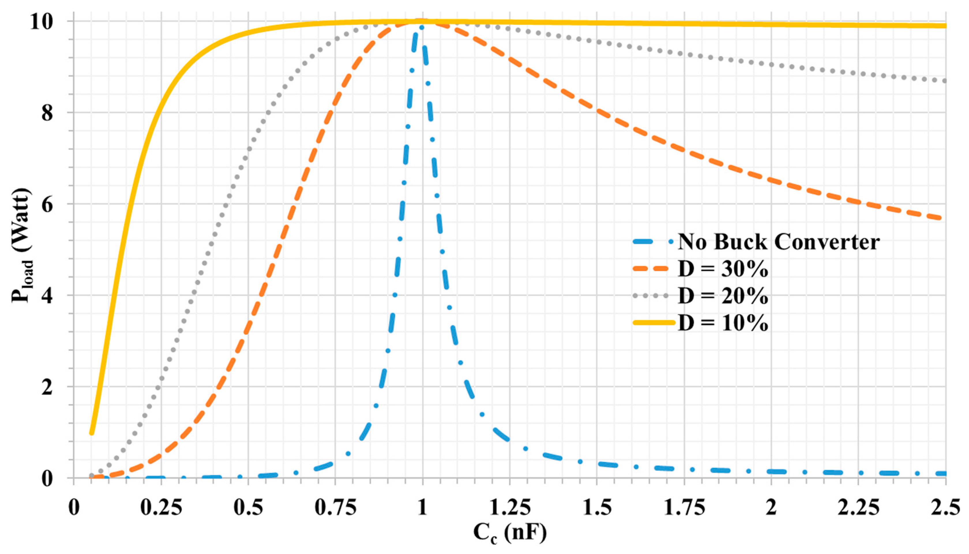
By reducing the system sensitivity, the system’s ability to transfer power becomes impervious to large parametric variations. Figure 5 shows the impacts on output power with changes in the capacitive coupling interface. For the conventional system, by changing the interface value by only 10% of its original value, no power will transfer to the load and resonance frequency will vary considerably due to the high Q. Conversely, by using the DC–DC buck converter on the power receiving side, the system becomes immune to parameter changes and the ability to transfer the power increases even under extreme conditions. For instance, if D = 10% is used, the power can be transferred with almost the same amount for any increase in the interface value from 250% more to 55% less than the original interface value by using DC–DC buck converter as a part of the secondary side. As such, the misalignment issue is of less concern.
By adding the buck converter, the Q value remained low for any value of the interface, as shown in Figure 6, which guarantees the system robustness. On the contrary, the previous system Q is susceptible to variations in the coupling interface, especially when the coupling capacitance is reduced to less than 0.5 nF.
The load can be a parameter that affects the system by changes that may occur due to the change in the battery under charge at the DC level, for example. Figure 7 shows that the Q value is stable and low for a wide range of changes in the load, unlike the case without DC–DC buck converter added where the Q reaches to more than 100 for some load values.
3.2. Voltage Stress Across the Capacitive Interface
By having the DC–DC buck converter on the secondary side in the proposed system, the equivalent AC load increased with decreasing D as expressed in Equation (4). Therefore, the input voltage had to be boosted accordingly per Equation (5) and the power could be transferred with smaller current (I) to the load in the same amount of transferred power. The current flowing through the interface (I) can be found using Equation (10), which can be expressed as a function of the duty cycle and the interface current of the conventional system at the resonance frequency, as shown in Equation (13). The reduction in the current through the circuit results in less voltage stress Vc across the one pair of the coupling plates as described in Equations (11) and (12). Figure 8 that shows how Vc varies with the duty cycle of the DC–DC converter. The voltage stress across one pair of the coupling plates (Vc) decreases proportionally with D at the resonant frequency, as given in Equation (14). At low frequencies, the terms can be neglected and Vc can be determined, as shown in Equation (15), which explains the high Vc at the low frequencies. According to these results, the probability of having safety issues or the occurrence of sparks and dielectric breakdown is much lower, and can be totally neglected if D is sufficiently low.
If the switching frequency = the resonance frequency,
If the switching frequency « the resonance frequency,
where Iconv and Vc_conv are the current flowing through the interface and the voltage across a single pair of the capacitive coupling interface plates for the conventional system, respectively.
4. Electric Field Simulation
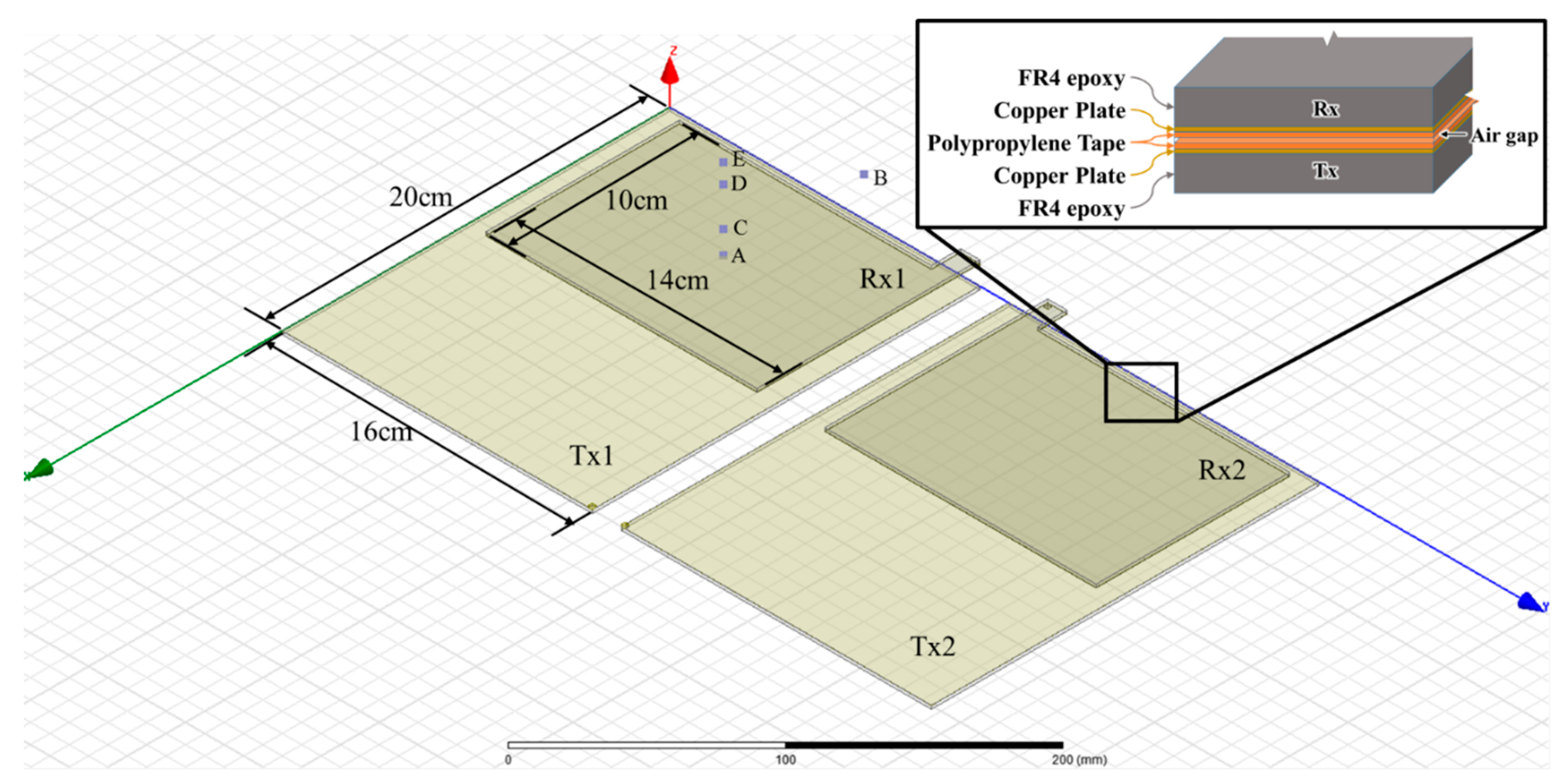
As discussed in the previous section, the proposed system has lower voltage stress over the capacitive coupling interface. Accordingly, the electric field in between the coupling plates, including the leakage electric field emissions, should decrease as well. In this section, the transient E field analysis in Maxwell software from Ansys, Pennsylvania, USA, was used to simulate the electric field strength between and around the plates. Figure 9 shows the experimental modelling used as the coupling interface with the same dimensions and materials. Measurement points were assigned between and at different distances around the plates as listed in Table 2.
Figure 10 shows that the electric field between the single pair coupling interface plates reduced by D factor, which results in a reduction in the electric field emission to the surrounding space as illustrated in Figure 11 and Figure 12.
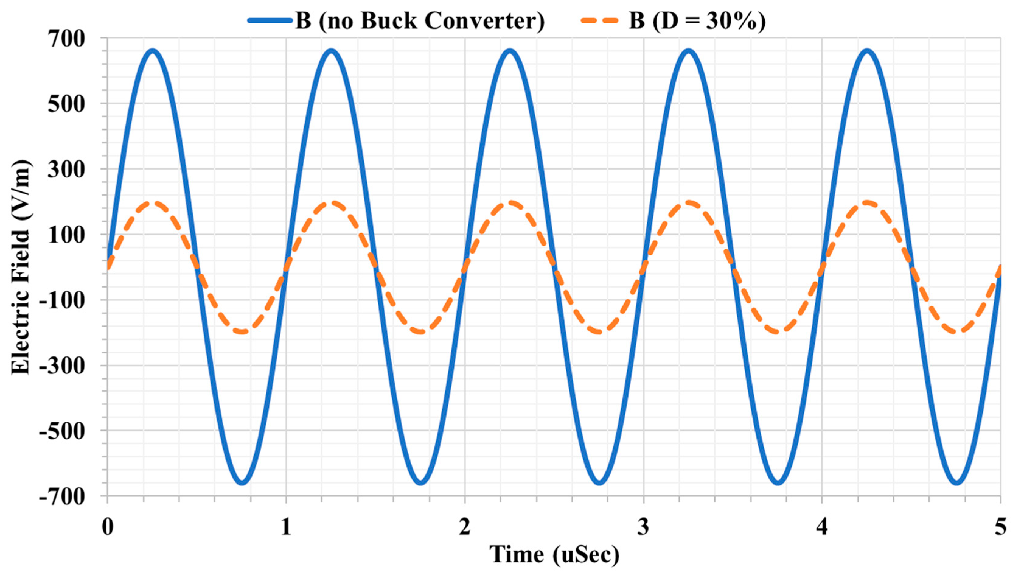
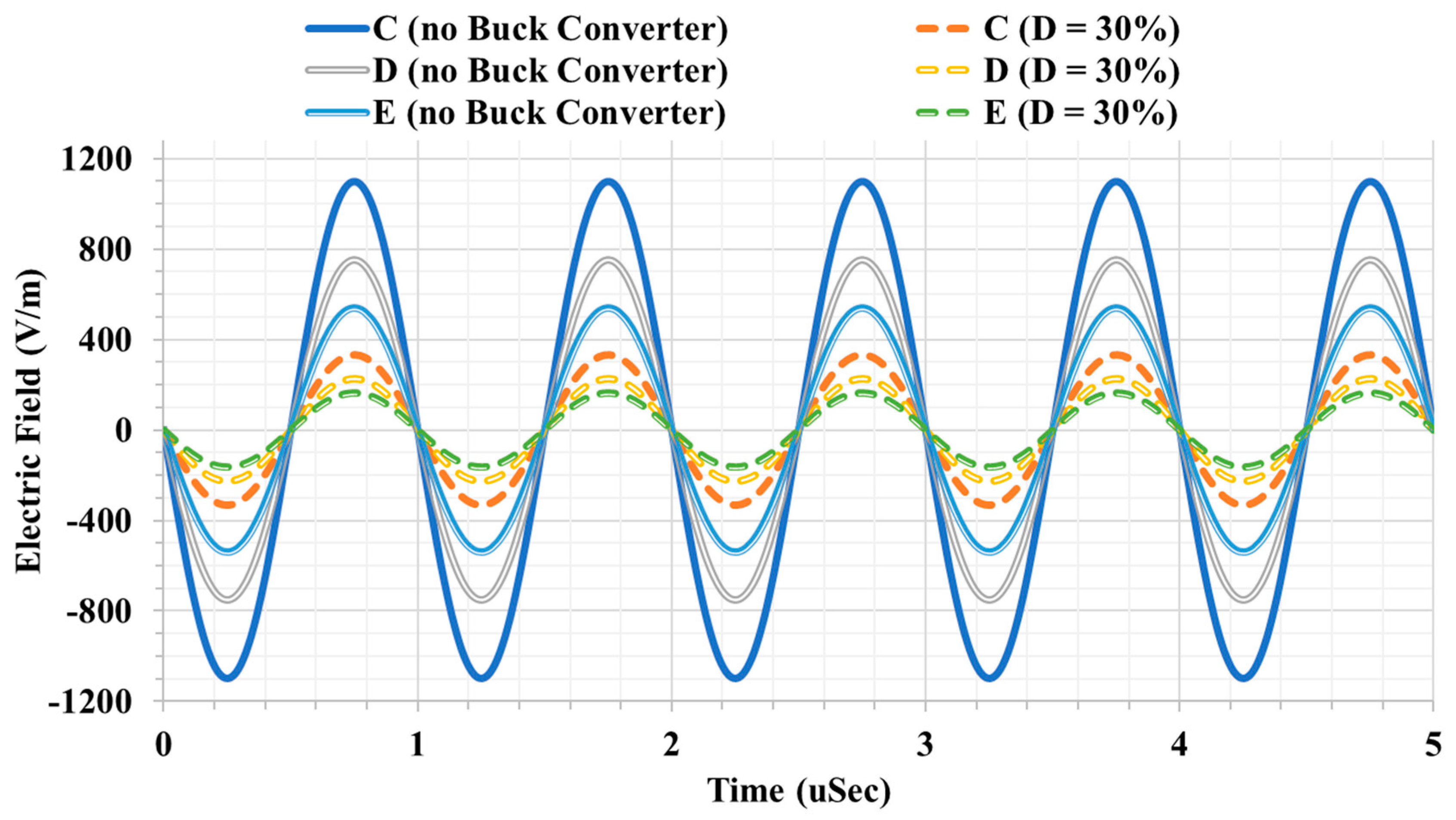
According to the Institute of Electrical and Electronics Engineers (IEEE) standard for safety levels with respect to human exposure to radio frequency electromagnetic fields of 3 kHz to 300 GHz [28], the field strength emissions for any system should be lower than 614 V/m for 0.03–1.34 MHz to ensure safe operation without harm to the human body. According to Figure 11, for the conventional CPT, the safe region starts after 2.5 cm in the X and Y directions from the plates by adding a buck converter electric field lower than 614 V/m anywhere in the XY plane around the plates. Figure 12 shows that the safe region for the conventional system, where the electric field is acceptable, is 3.5 cm above the plates. Notably, the system with a buck converter has sufficiently low electric field levels to be used safely. The proposed system helps to safely use CPT technology without the need for shielding or living object detection systems.
5. Experimental Results
A prototype was built, based on parameters listed in Table 3, as shown in Figure 13. The capacitive coupling interface was made of copper boards and the metal faces are covered by the polypropylene tape (relative permittivity is about 2.5) as a dielectric material. The dimensions of the pickup plates were chosen to suit the back side of an Apple 10-inch iPad, 10 cm × 14 cm each. Four Schottky diodes were used to compose the rectifier for its high-frequency abilities, and Litz-wire was used for inductors to reduce skin effect. Duty cycles 20%, 30% and 100% (system without buck converter) of DC–DC buck converter were examined. The input voltage value was determined according to the duty cycle used in the DC–DC buck converter for delivering 10 W of power to the load. The frequency was swiped from 0.35 MHz to 2.5 MHz to show the frequency responses of the output power and the voltage stress across the interface.
For kilowatt (kW) level high power applications, silicon-carbide (SiC) field effect transistors (FETs) can be used instead of conventional power metal oxide semiconductor field effect transistor (MOSFETs) used in this experiment; while at low power high frequency operations at several tens of MHz, gallium-nitride (GaN) FETs provides a good option [29].
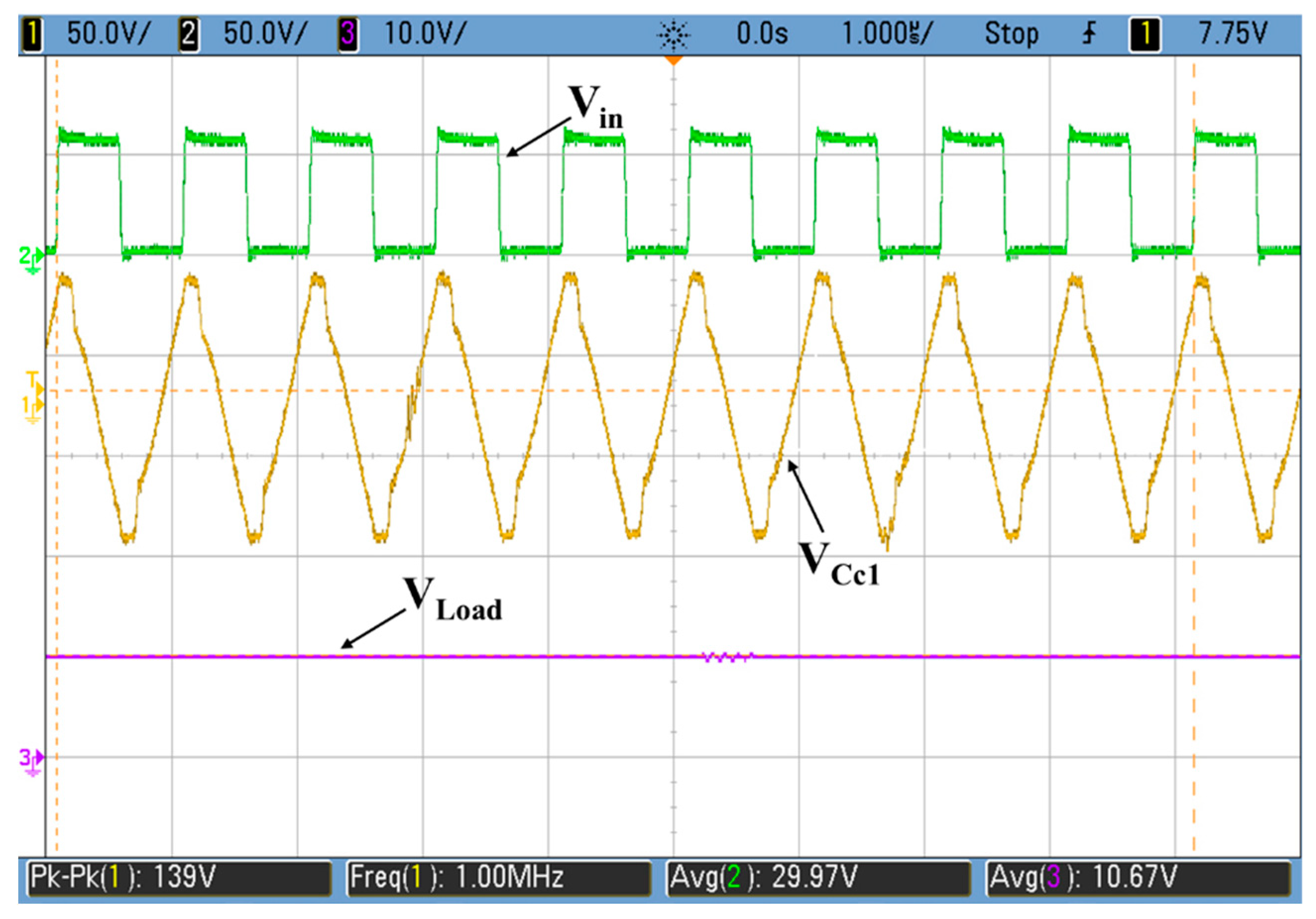
Figure 14 shows the frequency response of the DC output power at different duty cycles. Q reduction is confirmed by reducing the duty cycle of the buck converter as predicted from the analysis. The main reason for the shift in the response is the change in the value of the total impedance of the load and the parasitic capacitance of the diodes that constructs the rectifier by changing the duty cycle. As proved in the analysis section, by reducing Q, the system’s tolerance to misalignment improves, as shown in Figure 15. Figure 16 shows the amplitude of voltage stress measured across the single pair of the capacitive interface (Cc1). A differential probe was used to eliminate the common ground effect. The voltage stress is proportionally decreasing with the duty cycle which follows Equation (14) from the mathematical analysis. The maximum voltage stress across the capacitive interface (Cc1) is reduced to about 65 V at D = 30% and 44 V at D = 20%, corresponding to an output power of 10 W, while 211 V is measured for the no buck converter used case. The values of the experimental results of Vc is higher than the calculated ones due to the non-ideal components in the system and the switching losses which decrease the efficiency, so a higher input voltage is needed to deliver 10 W resulting in higher voltage stress across the interface. By using 64 V DC input voltage (VD), the system could deliver 10 W of power at the duty cycle of 30% and operating frequency 1 MHz, while the end-to-end system efficiency reached 80%. Figure 17 shows the measured Vin, Vc, and Vout.
6. Conclusions
This paper proposed a novel method for reducing the voltage stress and sensitivity of a CPT system by using a DC–DC buck converter. Mathematical analysis of the proposed system has been carried out to investigate the change in the system’s Q and the voltage stress across the coupling interface. The leakage electric field emissions were simulated by using the Maxwell software package. It is found that by reducing the duty cycle of the DC–DC buck converter, the system Q reduces proportionally to D2. Accordingly, the system tolerance to the change in the system parameters has improved. While transferring the same amount of power, the voltage stress is reduced proportionally to D and the related leakage electric field around the plates is drastically shrunk so the system becomes safer and the probability of dielectric breakdown or spark occurrence becomes much less. The experimental results from a 10 W CPT prototype demonstrated that by adding the buck converter, Q and voltage stress could effectively be reduced by changing the duty cycle. The maximum voltage stress across one pair of the coupling plates has been reduced to 65 V and 44 V at duty cycles of 30% and 20%, respectively, compared to 211 V for the conventional system without using a DC–DC converter. By applying 64 V input DC voltage and 30% buck converter duty cycle the system has achieved a system input to output (end-to-end) power efficiency of 80% at an output power of 10 W.
Author Contributions
T.M. proposed the idea, obtained the results, and wrote the paper. T.M. and D.B. built the experimental setup. All authors together contributed by drafting and critical revisions.
Funding
This research received no external funding.
Conflicts of Interest
The authors declare no conflict of interest.
References
- Tesla, N. Electrical Transformer or Induction Device. U.S. Patent No. 433,702, 5 August 1890. [Google Scholar]
- Hu, A.P. Wireless/Contactless Power Supply—Inductively Coupled Resonant Converter Solutions; VDM Verlag Dr Mueller: Saarbrücken, Germany, 2009; ISBN 978-3-639-11673-1. [Google Scholar]
- Green, A.W.; Boys, J.T. 10 kHz Inductively Coupled Power Transfer-Concept and Control. In Proceedings of the 1994 Fifth International Conference on Power Electronics and Variable-Speed Drives, London, UK, 26–28 October 1994; pp. 694–699. [Google Scholar]
- Hui, S.Y.R.; Ho, W.W.C. A new generation of universal contactless Battery Charging platform for portable Consumer Electronic equipment. IEEE Trans. Power Electron. 2005, 20, 620–627. [Google Scholar] [CrossRef]
- Covic, G.A.; Boys, J.T.; Kissin, M.L.G.; Lu, H.G. A three-phase inductive power transfer system for roadway-powered vehicles. IEEE Trans. Ind. Electron. 2007, 54, 3370–3378. [Google Scholar] [CrossRef]
- Thrimawithana, D.J.; Madawala, U.K. A Three-Phase Bi-Directional IPT System for Contactless Charging of Electric Vehicles. In Proceedings of the 2011 IEEE International Symposium on Industrial Electronics, Gdansk, Poland, 27–30 June 2011. [Google Scholar]
- Hu, A.P.; You, Y.W.; Chen, F.Y.B.; McCormick, D.; Budgett, D.M. Wireless Power Supply for ICP Devices with Hybrid Supercapacitor and Battery Storage. IEEE J. Emerg. Sel. Top. Power Electron. 2016, 4, 273–279. [Google Scholar] [CrossRef]
- Kurs, A.; Karalis, A.; Moffatt, R.; Joannopoulos, J.D.; Fisher, P.; Soljačić, M. Wireless power transfer via strongly coupled magnetic resonances. Science 2007, 317, 83–86. [Google Scholar] [CrossRef] [PubMed]
- Karalis, A.; Joannopoulos, J.D.; Soljačić, M. Efficient wireless non-radiative mid-range energy transfer. Ann. Phys. 2008, 323, 34–48. [Google Scholar] [CrossRef] [Green Version]
- Chao, L.; Hu, A.P.; Wang, B.; Nair, N.C. A Capacitively Coupled Contactless Matrix Charging Platform with Soft Switched Transformer Control. IEEE Trans. Ind. Electron. 2013, 60, 249–260. [Google Scholar] [CrossRef]
- Liu, C.; Hu, A.P. Wireless/Contactless Power Transfer-Capacitevely Coupled Solutions; LAP Lambert Academic Publishing: Saarbrucken, Germany, 2012. [Google Scholar]
- Mostafa, T.M.; Muharam, A.; Hattori, R. Wireless Battery Charging System for Drones via Capacitive Power Transfer. In Proceedings of the 2017 IEEE PELS Workshop on Emerging Technologies: Wireless Power Transfer (WoW), Chongqing, China, 20–22 May 2017; pp. 1–6. [Google Scholar]
- Liu, C.; Hu, A.P. Power Flow Control of a Capacitively Coupled Contactless Power Transfer System. In Proceedings of the 2009 35th Annual Conference of IEEE Industrial Electronics, Porto, Portugal, 3–5 November 2009; pp. 743–747. [Google Scholar]
- Huang, L.; Hu, A.P. Defining the mutual coupling of capacitive power transfer for wireless power transfer. Electron. Lett. 2015, 51, 1806–1807. [Google Scholar] [CrossRef]
- Culurciello, E.; Andreou, A.G. Capacitive Inter-Chip Data and Power Transfer for 3-D VLSI. IEEE Trans. Circuits Syst. II Expr. Briefs 2006, 53, 1348–1352. [Google Scholar] [CrossRef]
- Salzman, D.; Knight, T., Jr.; Franzon, P. Application of Capacitive Coupling to Switch Fabrics. In Proceedings of the 1995 IEEE Multi-Chip Module Conference (MCMC-95), Santa Cruz, CA, USA, 31 January–2 February 1995; pp. 195–199. [Google Scholar]
- Wang, K.; Sanders, S. Contactless USB—A Capacitive Power and Bidirectional Data Transfer System. In Proceedings of the 2014 IEEE Applied Power Electronics Conference and Exposition—APEC 2014, Fort Worth, TX, USA, 16–20 March 2014; pp. 1342–1347. [Google Scholar]
- Muharam, A.; Mostafa, T.M.; Hattori, R. Design of Power Receiving Side in Wireless Charging System for UAV Application. In Proceedings of the 2017 International Conference on Sustainable Energy Engineering and Application (ICSEEA), Jakarta, Indonesia, 23–24 October 2017; pp. 133–139. [Google Scholar]
- Hu, A.P.; Liu, C.; Li, H.L. A Novel Contactless Battery Charging System for Soccer Playing Robot. In Proceedings of the 2008 15th International Conference on Mechatronics and Machine Vision in Practice, Auckland, New Zealand, 2–4 December 2008; pp. 646–650. [Google Scholar]
- Kim, J.; Bien, F. Electric Field Coupling Technique of Wireless Power Transfer for Electric Vehicles. In Proceedings of the IEEE 2013 Tencon-Spring, Sydney, NSW, Australia, 17–19 April 2013; pp. 267–271. [Google Scholar]
- Lu, F.; Zhang, H.; Hofmann, H.; Mi, C. A Double-Sided LCLC-Compensated Capacitive Power Transfer System for Electric Vehicle Charging. IEEE Trans. Power Electron. 2015, 30, 6011–6014. [Google Scholar] [CrossRef]
- Bowick, C. Resonant Circuits. In RF Circuit Design, 2nd ed.; Elsevier/Newnes: New York, NY, USA, 2008; Chapter 2; pp. 26–28. ISBN 9780750685184. [Google Scholar]
- Theodoridis, M.P. Effective Capacitive Power Transfer. IEEE Trans. Power Electron. 2012, 27, 4906–4913. [Google Scholar] [CrossRef]
- Funato, H.; Kobayashi, H.; Kitabayashi, T. Analysis of Transfer Power of Capacitive Power Transfer System. In Proceedings of the 2013 IEEE 10th International Conference on Power Electronics and Drive Systems (PEDS), Kitakyushu, Japan, 22–25 April 2013; pp. 1015–1020. [Google Scholar]
- Kline, M.; Izyumin, I.; Boser, B.; Sanders, S. Capacitive Power Transfer for Contactless Charging. In Proceedings of the 2011 Twenty-Sixth Annual IEEE Applied Power Electronics Conference and Exposition (APEC), Fort Worth, TX, USA, 6–11 March 2011; pp. 1398–1404. [Google Scholar]
- Erickson, R.W.; Maksimovic, D. Resonant Conversion. In Fundamentals of Power Electronics, 2nd ed.; Kluwer Academic: New York, NY, USA, 2001; Chapter 19; pp. 711–713. [Google Scholar]
- Zhang, H.; Lu, F.; Hofmann, H.; Liu, W.; Mi, C. A Large Air-Gap Capacitive Power Transfer System with a 4-Plate Capacitive Coupler Structure for Electric Vehicle Charging Applications. In Proceedings of the 2016 IEEE Applied Power Electronics Conference and Exposition (APEC), Long Beach, CA, USA, 20–24 March 2016; pp. 1726–1730. [Google Scholar] [CrossRef]
- IEEE Standards Association. IEEE Standard for Safety Levels with Respect to Human Exposure to Radio Frequency Electromagnetic Fields, 3 kHz to 300 GHz; IEEE Standard C95.1; IEEE: Piscataway, NJ, USA, 2005. [Google Scholar]
- Taranovich, S. Si vs. GaN vs. SiC: Which Process and Supplier Are Best for My Power Design? EDN NETWORK. 15 March 2013 [Online]. Available online: https://www.edn.com/design/power-management/4409627/Si-vs--GaN-vs--SiC--Which-process-and-supplier-are-best-for-my-power-design- (accessed on 14 April 2018).
Figure 1.
The conventional capacitive power transfer (CPT) system.

Figure 2.
The proposed system: (a) CPT system with a DC–DC buck converter; (b) circuit simplification by the sinusoidal approximation, and (c) equivalent circuit used for analysis.
Figure 2.
The proposed system: (a) CPT system with a DC–DC buck converter; (b) circuit simplification by the sinusoidal approximation, and (c) equivalent circuit used for analysis.
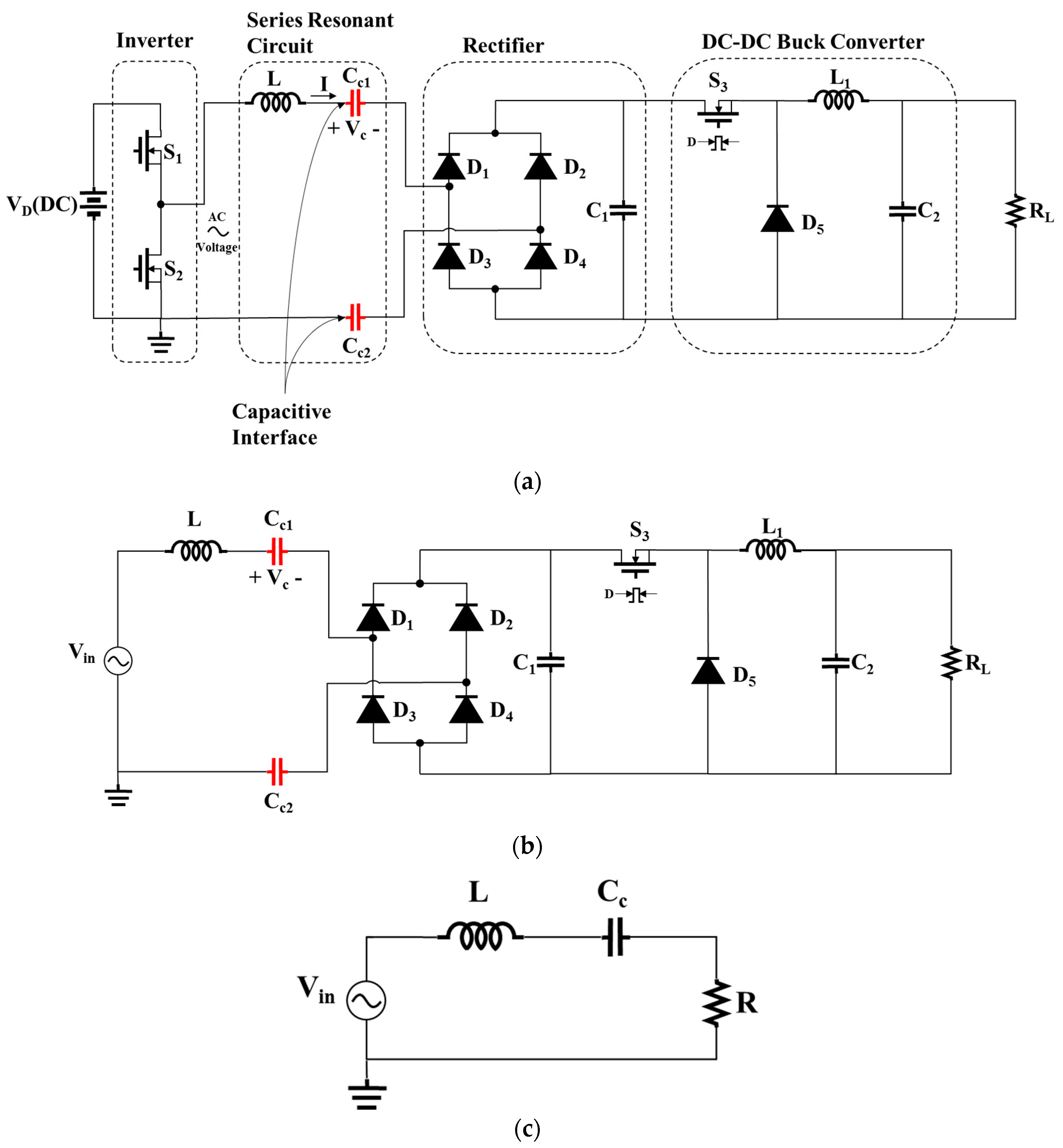
Figure 3.
Input voltage needed to deliver 10 W to the load and the change in the quality factor of the circuit Q with different duty cycles D.
Figure 3.
Input voltage needed to deliver 10 W to the load and the change in the quality factor of the circuit Q with different duty cycles D.

Figure 4.
The frequency response of the output power at different duty cycles D.
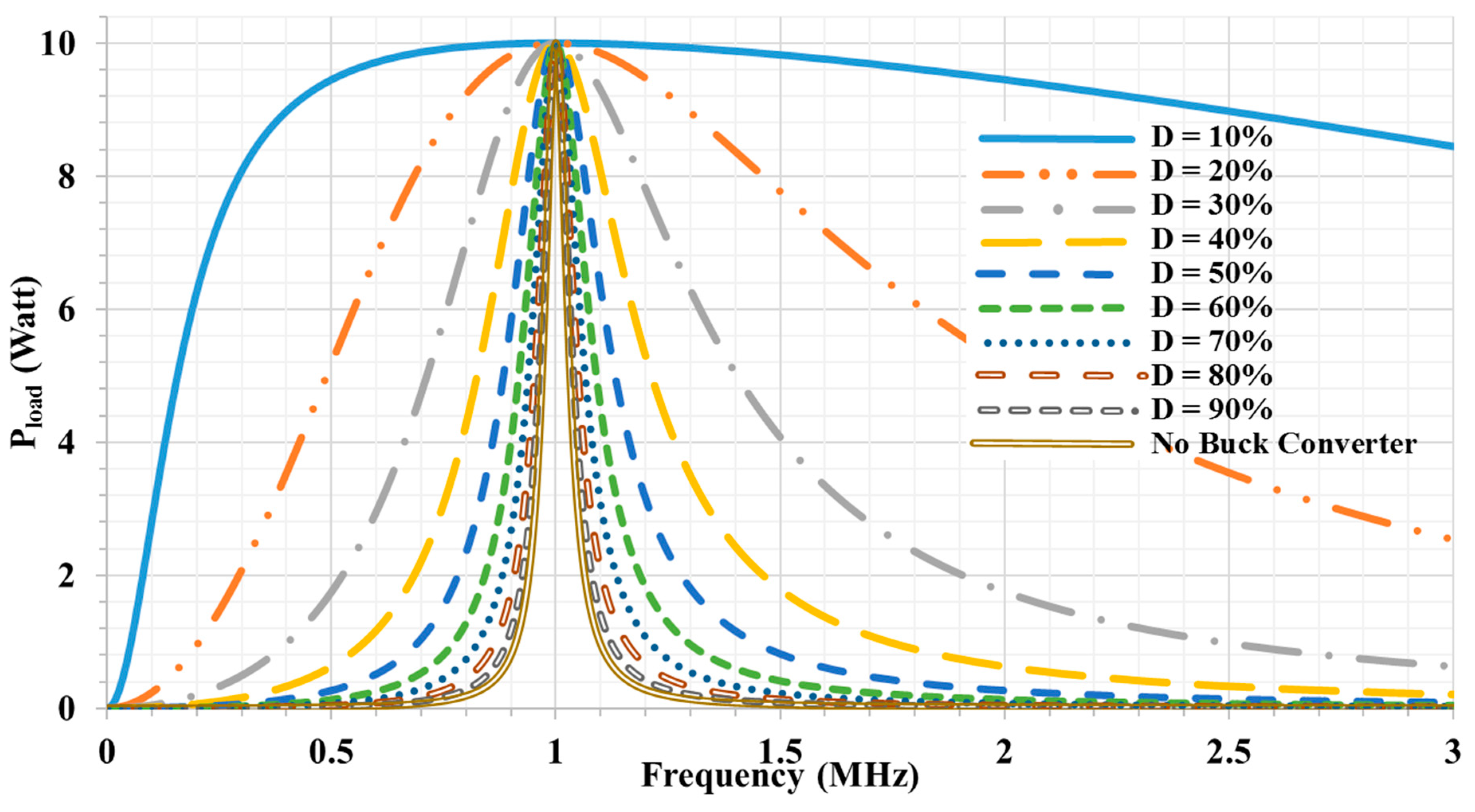
Figure 5.
The tolerance of the output power with the change in the capacitive interface value using different duty cycles D.
Figure 5.
The tolerance of the output power with the change in the capacitive interface value using different duty cycles D.

Figure 6.
The change in the capacitive interface value effect on the Q value.
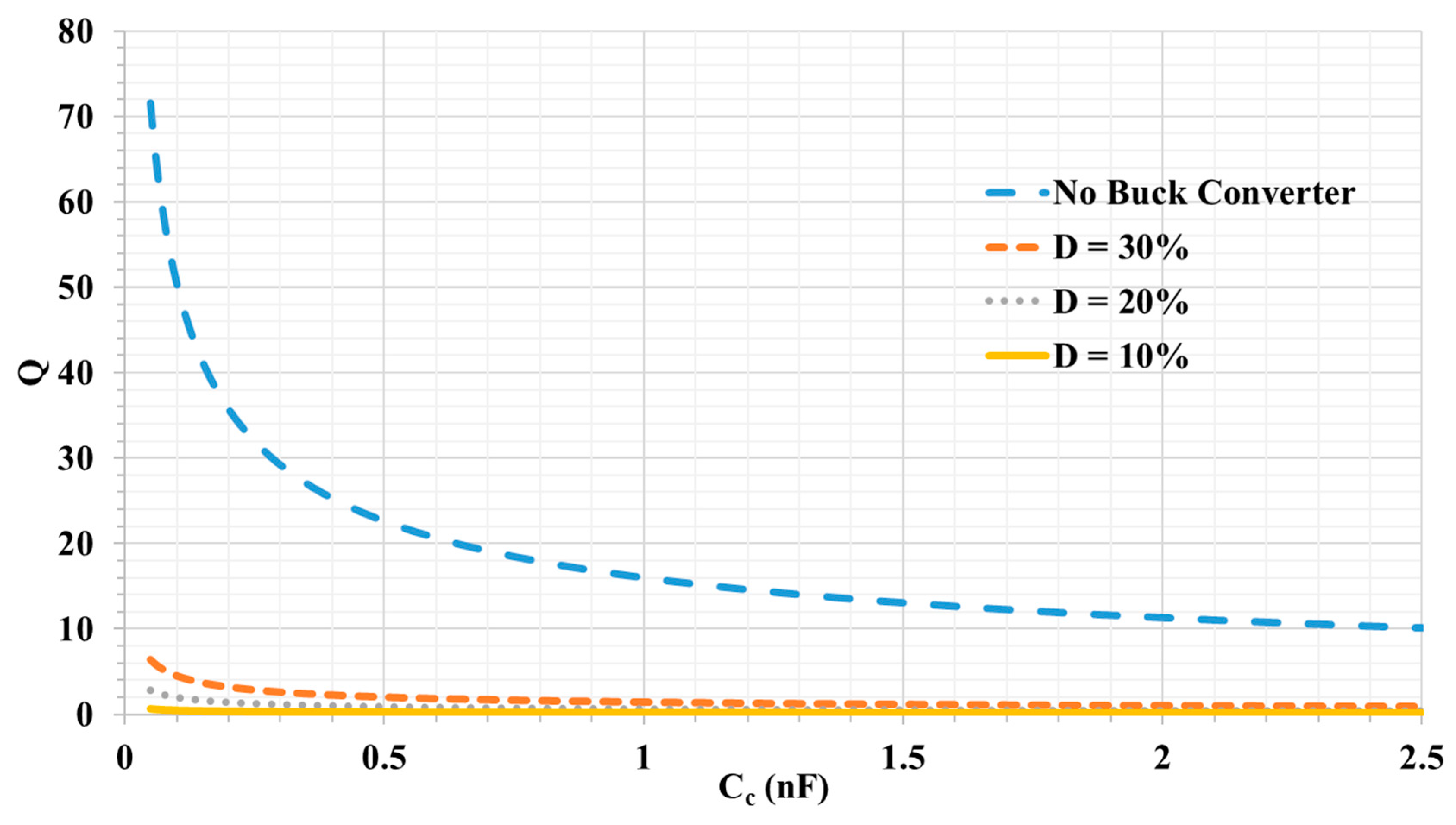
Figure 7.
Q value change with the load.

Figure 8.
The frequency response of the voltage Vc across one pair of the coupling plates at different duty cycles D.
Figure 8.
The frequency response of the voltage Vc across one pair of the coupling plates at different duty cycles D.
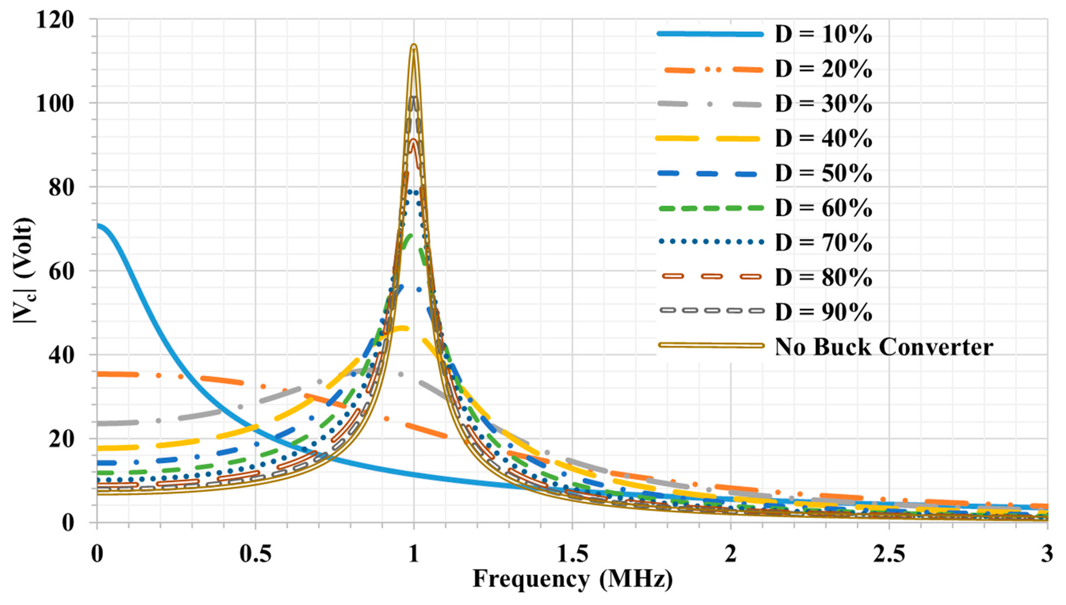
Figure 9.
Plates modelling in Ansys Maxwell.

Figure 10.
Simulated electric field at measure point A between Tx1 and Rx1.

Figure 11.
Simulated electric field at measurement point B in front of Tx1 and Rx1.

Figure 12.
Simulated electric field at measurement points C, D, and E above the center of Tx1 and Rx1.
Figure 12.
Simulated electric field at measurement points C, D, and E above the center of Tx1 and Rx1.

Figure 13.
The system prototype. PWM: pulse-width modulation.
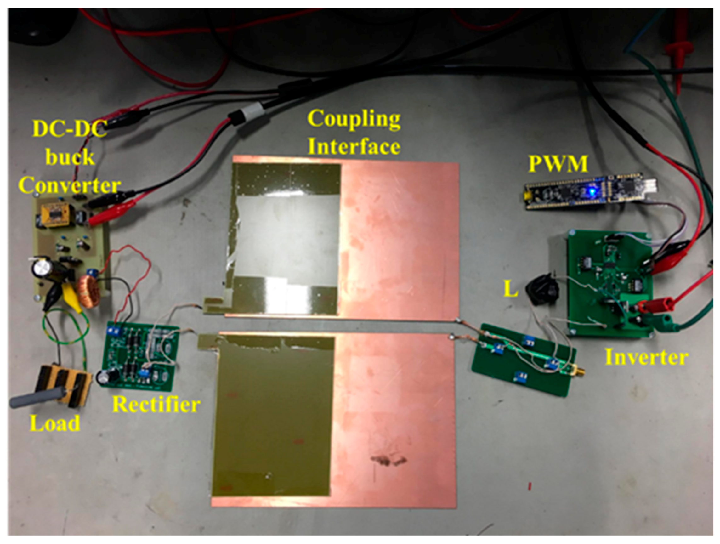
Figure 14.
Frequency response of the DC output power.
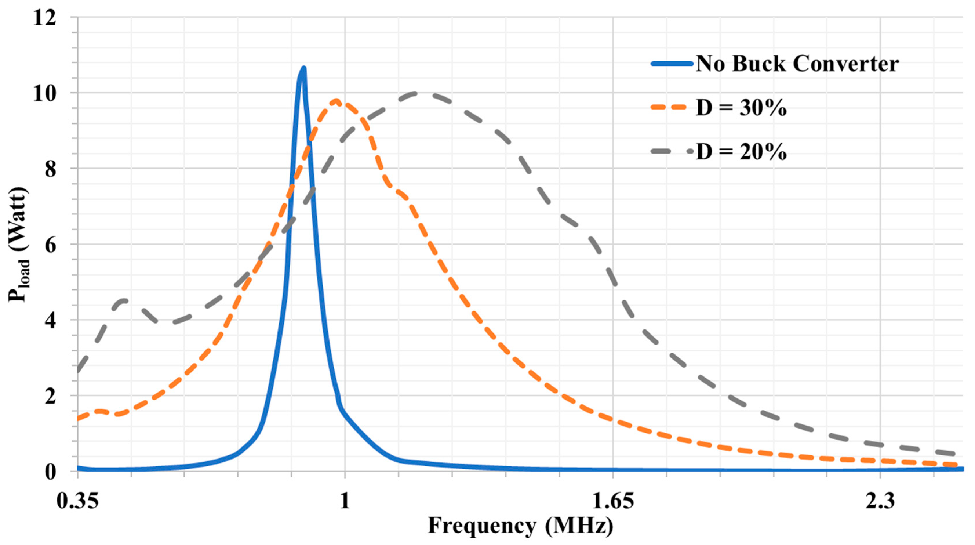
Figure 15.
The tolerance of the output power with the change in the capacitive interface equivalent series value.
Figure 15.
The tolerance of the output power with the change in the capacitive interface equivalent series value.
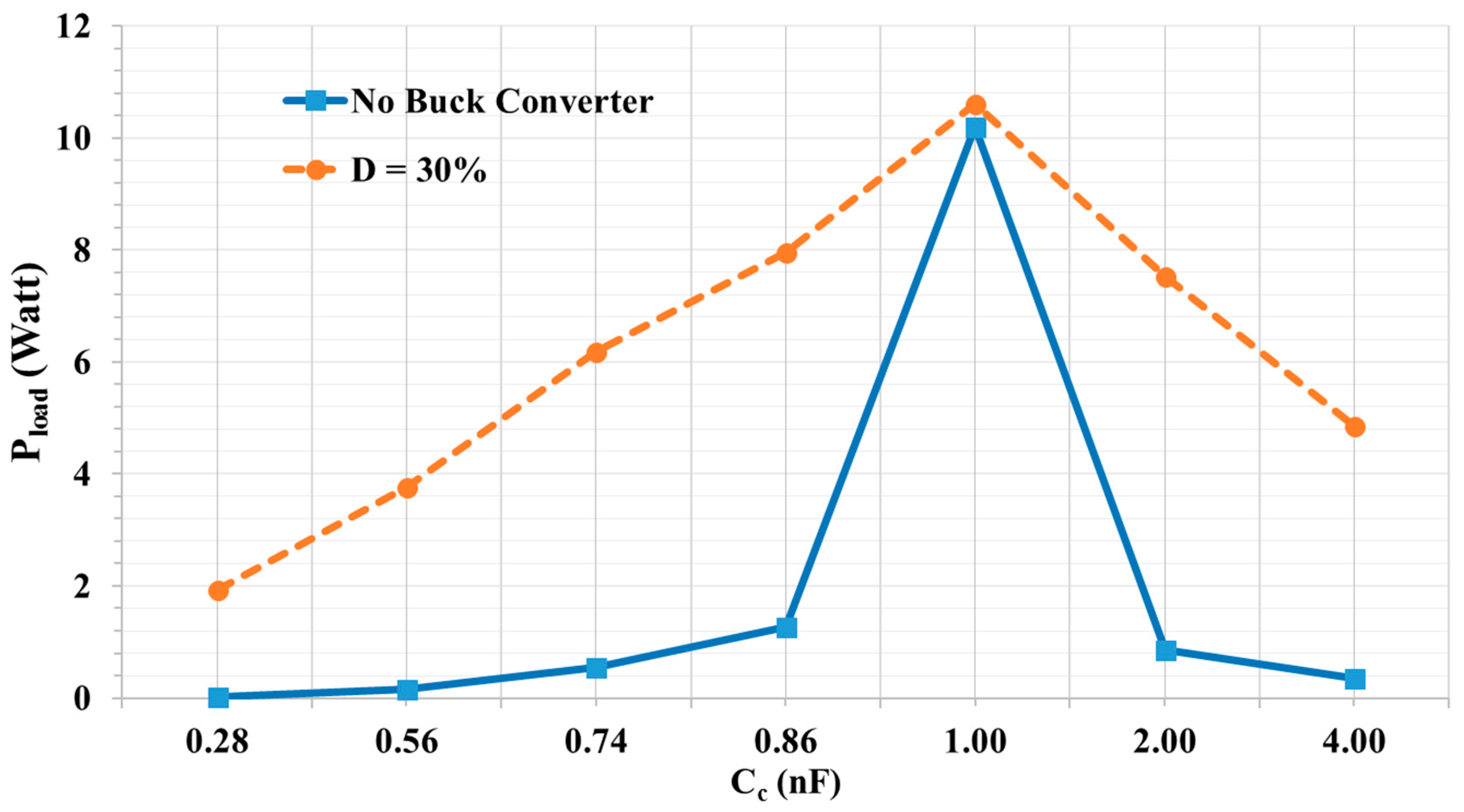
Figure 16.
Frequency response of the voltage across the single pair of the capacitive interface Cc1 (amplitude).
Figure 16.
Frequency response of the voltage across the single pair of the capacitive interface Cc1 (amplitude).
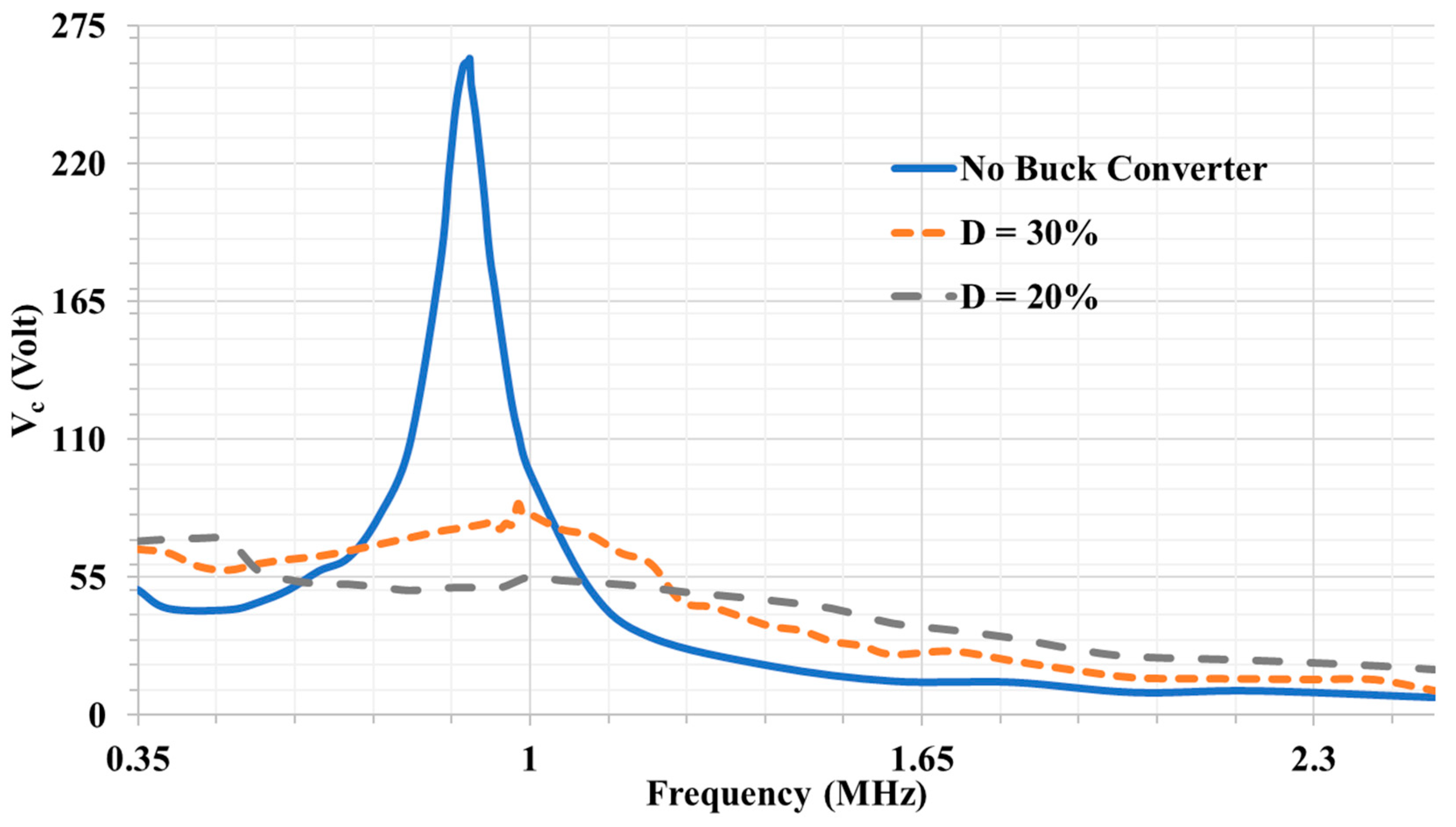
Figure 17.
Waveforms of the input AC voltage, voltage across the coupling capacitor, and the DC output voltage.
Figure 17.
Waveforms of the input AC voltage, voltage across the coupling capacitor, and the DC output voltage.


Table 1.
Parameters used for modelling.
| Parameter | Unit | Value |
|---|---|---|
| Watt | 10 | |
| MHz | 1 | |
| = 2Cc | nF | 2 |
| µH | 25 | |
| Ω | 10 |
Table 2.
Measurement points coordination.
| Point | Distance to the Plates (cm) X, Y, Z |
|---|---|
| A | In the center between Tx1 and Rx1 |
| B | 2, 0, 0 (in front of Tx1 and Rx1) |
| C | 0, 0, 1 (above the center of Tx1 and Rx1) |
| D | 0, 0, 3 (above the center of Tx1 and Rx1) |
| E | 0, 0, 4 (above the center of Tx1 and Rx1) |
Table 3.
Circuit parameters and system specifications.
| Parameter | Unit | Value |
|---|---|---|
| Watt | 10 | |
| MHz | 1 | |
| nF | ~2.1 | |
| nF | ~1.9 | |
| Duty Cycle | % | 20, 30, 100 |
| µH | 25 | |
| Ω | 10 |
© 2018 by the authors. Licensee MDPI, Basel, Switzerland. This article is an open access article distributed under the terms and conditions of the Creative Commons Attribution (CC BY) license (http://creativecommons.org/licenses/by/4.0/).
Share and Cite
MDPI and ACS Style
Mostafa, T.M.; Bui, D.; Muharam, A.; Hattori, R.; Hu, A.P. Capacitive Power Transfer System with Reduced Voltage Stress and Sensitivity. Appl. Sci. 2018, 8, 1131. https://doi.org/10.3390/app8071131
AMA Style
Mostafa TM, Bui D, Muharam A, Hattori R, Hu AP. Capacitive Power Transfer System with Reduced Voltage Stress and Sensitivity. Applied Sciences. 2018; 8(7):1131. https://doi.org/10.3390/app8071131
Chicago/Turabian StyleMostafa, Tarek M., Dai Bui, Aam Muharam, Reiji Hattori, and Aiguo Patrick Hu. 2018. "Capacitive Power Transfer System with Reduced Voltage Stress and Sensitivity" Applied Sciences 8, no. 7: 1131. https://doi.org/10.3390/app8071131
Note that from the first issue of 2016, this journal uses article numbers instead of page numbers. See further details here.