Article

Printed Organic Complementary Inverter with Single SAM Process Using a p-type D-A Polymer Semiconductor

1
Research Center for Organic Electronics (ROEL), Yamagata University, 4-3-16, Jonan, Yonezawa, Yamagata 992-8510, Japan
2
Yokohama R&D Center, Mitsubishi Chemical Corporation, Kanagawa 227-8502, Japan
*
Authors to whom correspondence should be addressed.
Appl. Sci. 2018, 8(8), 1331; https://doi.org/10.3390/app8081331
Submission received: 10 July 2018 / Revised: 28 July 2018 / Accepted: 7 August 2018 / Published: 9 August 2018
(This article belongs to the Special Issue Semiconducting Polymer for Organic Transistors)

Abstract

:

Featured Application

Featured Application: Flexible Organic Integrated Circuits.

Abstract

The demonstration of the complementary integrated circuit using printing processes is indispensable for realizing electronic devices using organic thin film transistors. Although complementary integrated circuits have advantages such as low power consumption and a wide output voltage range, complementary integrated circuits fabricated by the printing method have problems regarding driving voltage and performance. Studies on fabrication processes of electronic circuits for printing technology, including optimization and simplification, are also important research topics. In this study, the fabrication process of the printed complementary integrated circuit was simplified by applying a p-type donor-acceptor (D-A) polymer semiconductor, which is not strongly affected by the electrode work function. An inverter circuit and the ring oscillator circuit were demonstrated using this process. The fabricated ring oscillator array showed excellent performance, with low voltage operation and low performance variation.

Graphical Abstract

1. Introduction

The advantage of employing polymer semiconductors in the organic transistor fabrication process is not only the improvement of the film-forming property due to the high viscosity of the semiconductor ink, but also the reduction of variation in the electrical characteristics [1] due to the formation of a uniform film. In addition, since polymer semiconductors generally have high heat resistance, they can withstand the heating process after the formation of organic semiconductors. Recently, very high performance, exceeding 10 cm2/Vs, has been reported due to annealing treatment and orientation control after film formation [2]. A printing fabrication process using organic materials that can be made into ink facilitates continuous large area device and mass production, and roll to roll (R2R) becomes possible by using a flexible substrate created in a low-temperature process [3,4,5,6]. In particular, device fabrication using an on-demand printing method such as ink-jet printing is the ultimate resource-saving process, and has the potential to be low cost [6,7,8,9,10,11,12]. An advantage of the complementary organic integrated circuit composed of p-type and n-type organic thin film transistors is that it has low power consumption and a high noise margin [13,14]. Therefore, it has the potential to be applied to a wide range of devices, including low power consumption devices driven by small batteries. On the other hand, since p-type and n-type semiconductors are fabricated through deposition methods, the number of fabrication steps is greater than those required for positive channel metal oxide semiconductor (p-MOS) and negative channel metal oxide semiconductor (n-MOS) configurations. In addition, to improve the transistor characteristics, it is necessary to match the work function of the source and drain electrodes with the highest occupied molecular orbital and lowest unoccupied molecular orbital (HOMO-LUMO) level of the semiconductor, and selection of the source and drain electrode material or electrode treatment with the self-assembled monolayer (SAM) is required. For this reason, in order to achieve both the performance of p-type and n-type organic thin-film transistors (OTFTs) in a complementary integrated circuit, two types of electrode materials or SAM materials are required, and the development of a simple fabrication process is an important task.
In this paper, complementary organic integrated circuits were demonstrated using p-type semiconductors, which are not significantly affected by the work function of the source and drain electrodes. The fabrication process used in this study was reduced in steps to about half compared with the complementary circuit using a stacked structure [15,16,17,18,19]. Further, the dynamic characteristics of the inverter circuit were evaluated using a five-stage ring oscillator.

2. Materials and Methods

2.1. Device Fabrication

Figure 1 shows the fabrication process flow diagram of an organic complementary integrated circuit with a top-gate bottom-contact (TGBC) structure. First, a parylene film (diX-SR, KISCO, Tokyo, Japan) was deposited on a glass substrate (Eagle XG, Corning Inc., Corning, NY, USA) with a thickness of 200 nm, using a Specialty Coating Systems Lab Coater 2 (model PDS 2010, SCS Coatings, Indianapolis, IN, USA), as a base layer. This base layer controls the wettability of the silver nanoparticle ink during ink-jet printing. Next, the silver nanoparticle ink (NPS-JL, Harima Chemical, Inc., Tokyo, Japan) was patterned using ink-jet printing (DMP-2831, FujiFilm Dimatix, Santa Clara, CA, USA) to form the source/drain electrodes. Subsequently, the substrate was heated at 120 °C for 30 min in air. The resistivity of the printed electrode was 9.5 Ω cm and the work function was 4.9 eV [20]. Next, a hydrophobic bank for controlling the printing area of the semiconductor inks was formed by a dispenser using a Teflon solution (Image Master 350PC, Musashi Engineering, Inc., Tokyo, Japan). Subsequently, to increase the adhesion between the hydrophobic bank and the lower layer, the substrate was heated at 100 °C for 30 min. Next, the source/drain electrode was surface treated with 4-methylbenzenethiol (4-MBT) through an immersion process. In the case of the immersion process, the 4-MBT was coated on the source and drain electrodes of p-type and n-type OTFTs. The p-type and n-type semiconductor inks were printed using a dispenser system with a stage temperature of 60 °C. After the printing of semiconductor ink, the devices were annealed in a nitrogen atmosphere at 150 °C for 30 min. As a gate-insulating layer, parylene (diX-SR) was formed with a thickness of 300 nm. Finally, silver nanoparticle ink was patterned as a gate electrode by ink-jet printing and then sintered at 120 °C for 30 min. In this study, the electrode shape was not controlled but a relatively thin gate dielectric can be used. This is because the parylene film used for the gate dielectric is uniformly deposited along the surface shape. If a printable gate dielectric is used, a technique to suppress the coffee ring effect [20,21,22] of the printed electrodes will be useful and improve the OTFT characteristics and yields.

2.2. Material Inks

Organic semiconductor inks: A p-type donor-acceptor (D-A) polymer semiconductor and an n-type low molecular semiconductor were used as the semiconductor materials. Each ink was prepared to be printed by a dispenser system. For the p-type semiconductor, based on D-A polymer (MOP-01, Mitsubishi Chemical Corporation, Tokyo, Japan) [23,24,25,26], mesitylene was used as a solvent. The p-type semiconductor was dissolved to 0.01 wt % at room temperature. Benzobisthiadiazole (BBT) based semiconductor TU-3 [18,27] (Future Ink Corporation, Yonezawa, Japan) and poly(α-methylstyrene) (PaMS: Sigma-Aldrich, Merck KGaA, Darmstadt, Germany) were blended for the n-type semiconductor, and 1-methylnaphthalene was used a solvent. The concentrations of these materials were 0.045 wt % for TU-3 and 0.015 wt % for PaMS, and they were dissolved on a hot-plate at 120 °C for 30 min. The p-type and n-type organic semiconductors used in this paper are materials that are poorly soluble in solvents such as 1-methoxy-2-propyl acetate (PGMEA), which are often used as a solvent for gate dielectric material. Therefore, we believe it will be possible to replace readily printable gate dielectrics.
Hydrophobic bank ink: As a hydrophobic bank ink for defining the printing area of the organic semiconductor, Teflon (AF1600X, Dupont, Wilmington, DE, USA) was dissolved in Fluorinert (FC-43, 3M Company, Maplewood, MN, USA) to 1 wt %.

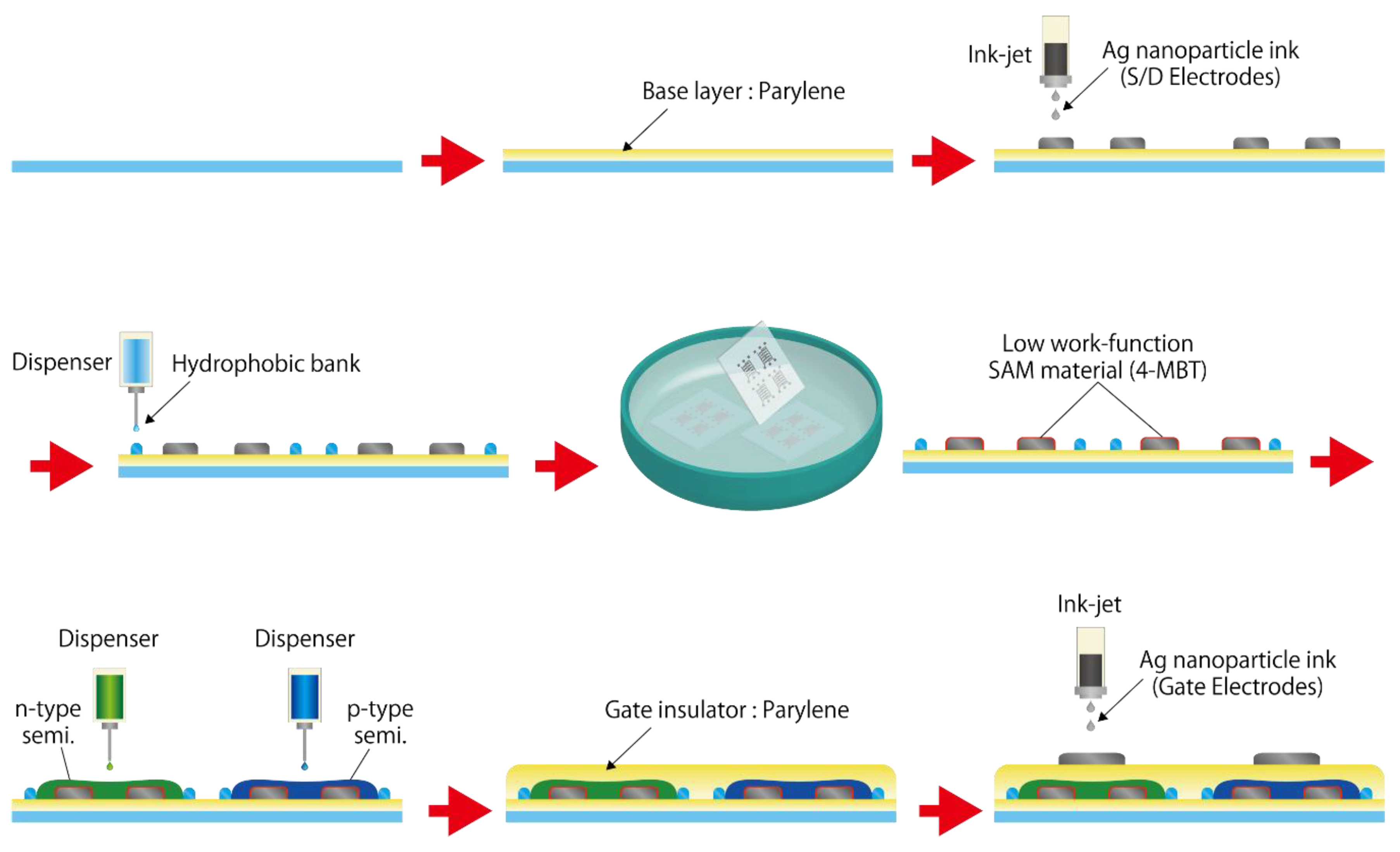
2.3. Complementary Integrated Circuit Fabrication Process

To fabricate a complementary inverter circuit, an electrode pattern was formed, in which the drains of p-type and n-type OTFTs were connected. In a ring oscillator circuit formed by connecting an odd number of inverter circuits, a via hole for the interlayer connection of electrodes is required. The via holes were formed using a YAG LASER (Light Amplification by Stimulated Emission of Radiation) system (VL-C30, V-Technology Co., Ltd., Yokohama, Japan), and the slit size for controlling the irradiation area was set to 50 × 75 μm. After opening the holes, the interlayer connection was made by filling silver nanoparticle ink using the ink-jet printing machine.

2.4. Device Characterization

A semiconductor parameter analyzer (4200A-scs, Keithley, Tektronix, Inc., Beaverton, OR, USA) was used to evaluate the static electrical characteristics of the fabricated OTFT and complementary inverter circuit. An oscilloscope (DSOS054A, Keysight, Santa Rosa, CA, USA) and high voltage probe (10076C, Keysight) with high input impedance and low input capacity were used for evaluating the output characteristics of the fabricated ring oscillator. The reason for using the high voltage probe is to reduce the influence of the probe on circuit operation. The work function of the electrodes was measured using photoemission yield spectroscopy in air (PYS) (AC-3, Riken, Saitama, Japan).

3. Results

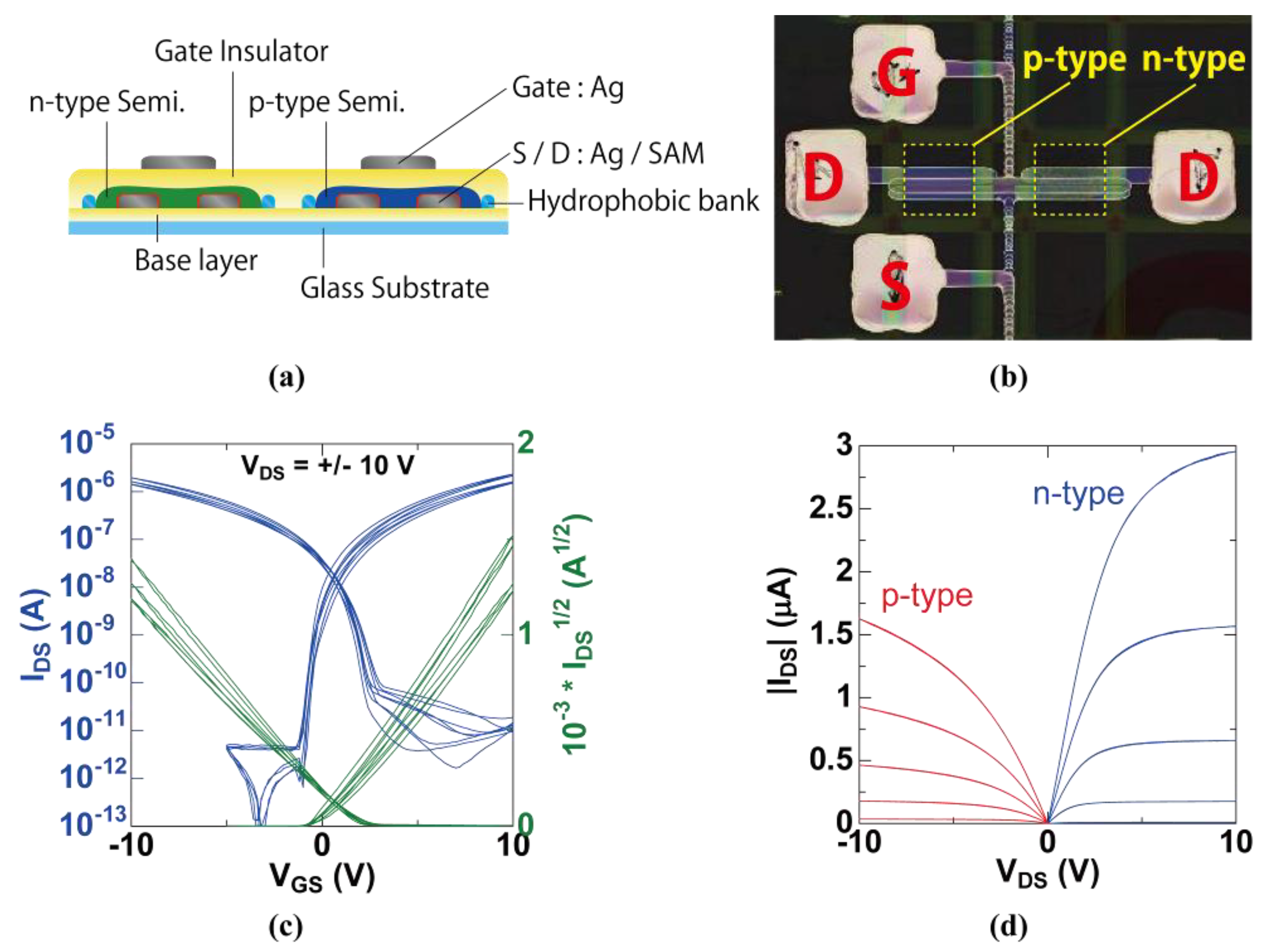
3.1. Fabrication of TGBC Structure Organic Complementary Integrated Circuits and OTFT Characteristics

The fabricated complementary integrated circuits have a top-gate bottom-contact structure in p-type and n-type OTFTs (Figure 2a). Figure 2b shows a microscope image of the fabricated complementary organic inverter circuit. In previous research, we adopted a stacked device structure to surface-functionalize the source/drain electrodes of p-type and n-type OTFTs with SAM materials separately [15,16,17,18,19]. However, this led to an increase in the number of device manufacturing steps and a reduction in yield. In this research, a complementary organic integrated circuit was realized by adapting a p-type D-A polymer semiconductor [21,22,23,24], which can obtain transistor characteristics even if it is modified with SAM material for an n-type semiconductor for the source/drain electrodes of the p-type OTFT. As a result, the complementary integrated circuit of this TG structure reduced the number of steps from 14 (in previous research) to seven, and succeeded in developing a simple process. The effect of treatment using the SAM material on a printed electrode was evaluated by photoelectron yield spectroscopy (PYS) in air. The work function of the untreated electrode was 4.8 eV, which was changed to 4.0 eV by 4-MBT treatment [18]. The transfer (Figure 2c) and output (Figure 2d) characteristics of the fabricated OTFTs that make up the integrated circuit were measured using a semiconductor parameter analyzer in ambient air conditions. The channel length (L) and width (W) ratio of the p-type and n-type OTFT devices was L/W = 29/960 μm. These OTFT devices exhibited excellent electrical performance at relatively low operating voltages of 10 V. For the p-type OTFT, the estimated hole mobility and threshold voltage were 0.11 cm2 V−1 s−1 and 0.09 V, respectively, and the on/off ratio was greater than 105. For the n-type OTFT, the estimated electron mobility and threshold voltage were 0.19 cm2 V−1 s−1 and 1.40 V, respectively, and the on/off ratio was greater than 107. These values were the averages of the four devices. Additionally, these advantageous output characteristics suggest that the contact resistance for each TFT device type is low. In many reports, there is a large difference in mobility between p-type and n-type OTFTs, and characteristics matching those of the OTFTs constituting the inverter circuit were required. This matching is important not only for correcting the switching point of the inverter characteristic, but also for correcting the deviation of the rise and fall time. However, in this study, since p-type and n-type OTFTs have almost equivalent mobility and threshold voltage, it is possible to realize a circuit with the same balance.

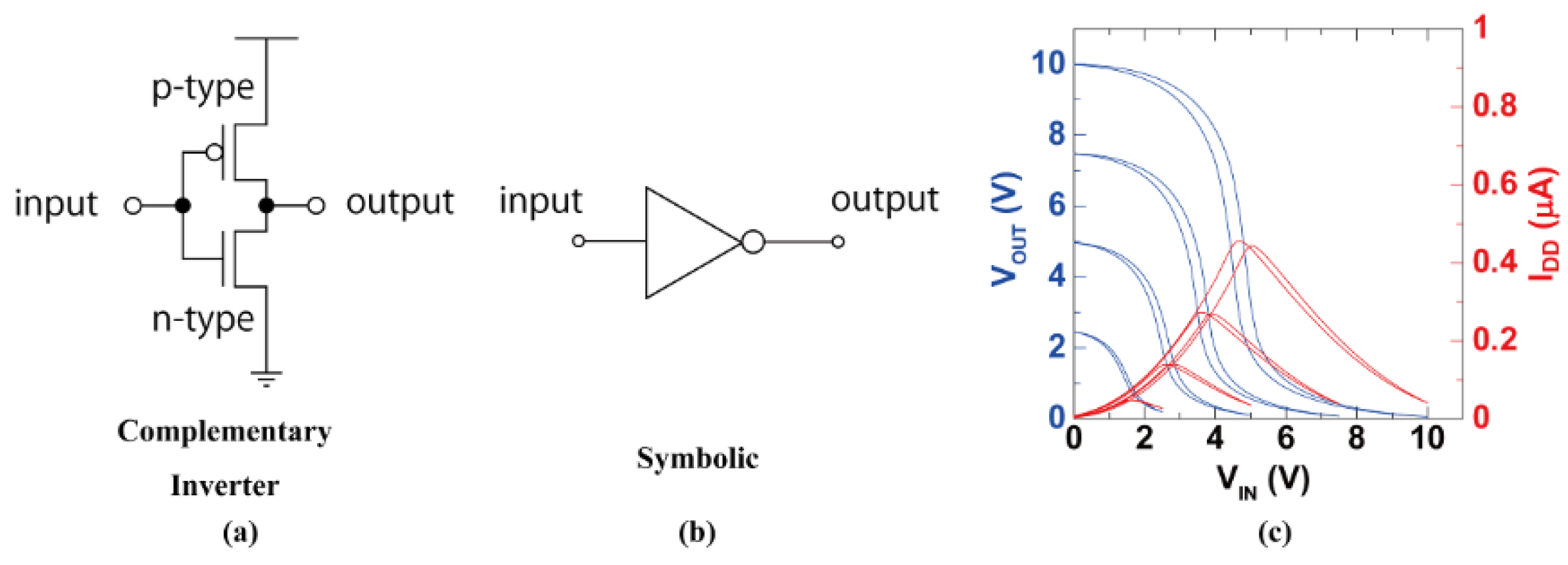
3.2. Electrical Performances of Organic Complementary Integrated Inverter Circuits

To investigate the feasibility of this study, we fabricated a complementary inverter circuit, which is the most basic circuit of organic integrated circuits. The inverter circuitry and its symbolic representation are shown in Figure 3a,b, respectively. In general, static performance is evaluated in inverter circuits. In this section, we evaluate gain, the switching (trip) point, and the noise margin from static characteristics. The performances of the inverter circuit static characteristics were evaluated as follows: the supply voltage (VDD) is kept constant, the input voltage (Vin) is swept, and the change in the output voltage (Vout) is measured.
Figure 3c shows the static (input/output) characteristic of the fabricated inverter circuit. The inverter circuit was driven excellently at an operating voltage of 1 to 10 V, the gain was 8.9 at an operating voltage of 10 V, the noise margin was 1.96 V (39%), and the hysteresis was low at this time. The noise margin of the fabricated inverter was less than 40% [18], which is lower than that in the previous report; however, this can be improved by adjusting the threshold voltage. Here, the signal gain is defined as the absolute value of dVout/dVin. The switching point is defined as the Vin at Vout = Vin. In an ideal inverter gate, the switching point should be equal to one half of VDD. The noise margin is defined as the side of the largest square that can be inscribed between the input-output characteristics. The maximum noise margin is equal to half of the supply voltage. The fabricated inverter circuit shows a noise margin greater than 50% at a VDD from 2.5 to 10 V. A summary of these characteristics is given in Table 1.

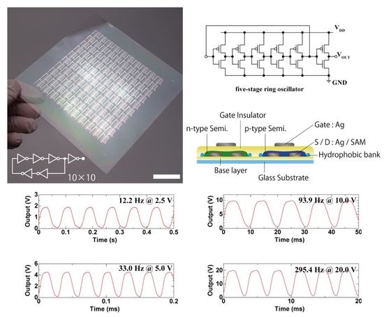
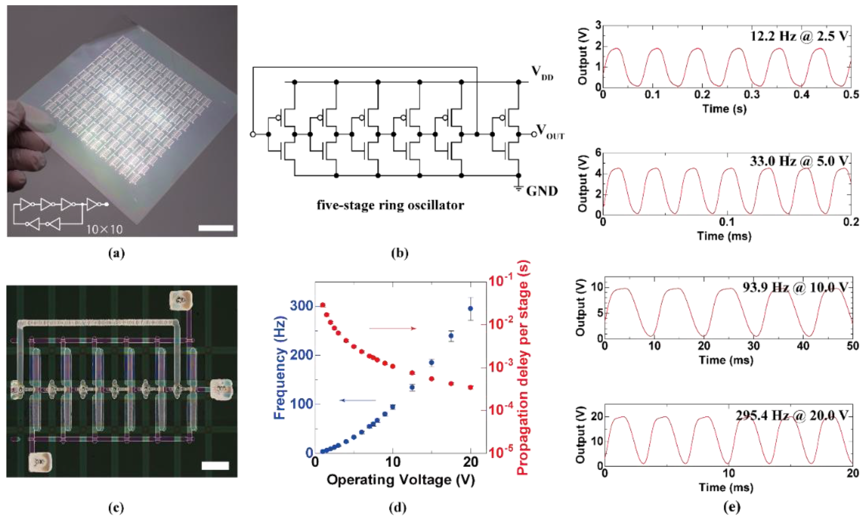
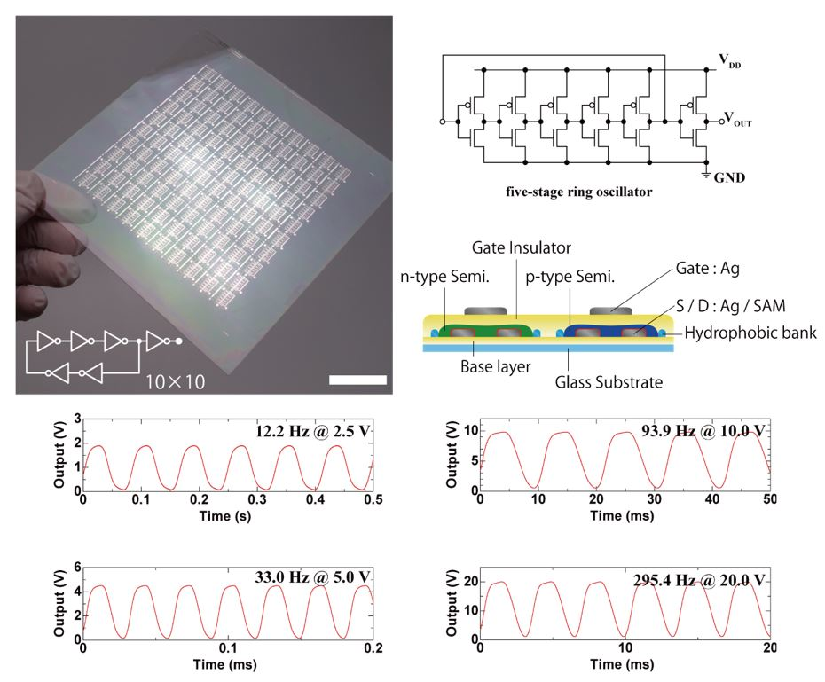
3.3. Fabrication and Characterization of Organic Complementary Ring Oscillator Array

Organic five-stage ring oscillators with a 10 × 10 device layout were fabricated, as shown in Figure 4a. By integrating an odd number of inverters, we were able to fabricate a ring oscillator circuit. The circuit diagram of the device is shown in Figure 4b. An optical microscope image of our ring oscillator is shown in Figure 4c. The average W/L values for p-type and n-type semiconductors were 960/60 and 960/55 μm, respectively. Oscillation frequency measurements were performed by measuring the voltage of the buffer inverter, whose input was driven by the oscillator output, using a digital oscilloscope with a high input impedance probe (66.7 MΩ, 3 pF). Figure 4d shows the signal propagation delays per stage and oscillation frequency measured with these ring oscillators plotted as a function of the operating voltage containing standard deviation error bars with 10 devices. The average value of the coefficient of variation, being the ratio of the magnitude of the data variation to the average, is 6.0%, showing that the variation is small. The measured stage delay is 28 ms at an operating voltage of 1 V, 8.2 ms at 2.5 V, 3.1 ms at 5 V, 1.7 ms at 7.5 V, 1.1 ms at 10 V, 0.54 ms at 15 V, and 0.34 ms at 20 V. The delay time of each inverter is defined as 1/2Nfosc, where N and fosc are the number of stages and the oscillation frequency, respectively. This value is a little slower than that in our previous research [18]. Comparing this delay time with the representative report results, ring oscillators fabricated by combining printed electrodes and semiconductors are in the high-speed class. Further high-speed operation can be expected by improving the mobility and shortening the channel by increasing the resolution of the source and drain electrodes. Figure 4e displays the output signal of the ring oscillator as a function of the operating voltages of 2 V, 5 V, 10 V, and 20 V.

4. Conclusions

We have fabricated complementary organic integrated circuits including inverter circuits and ring oscillators based on a p-type D-A polymer semiconductor with a TG structure for both p-type and n-type OTFTs. This complementary organic integrated circuit fabrication process using printed electrodes could dramatically reduce the number of steps compared to the previous fabrication process with a stacked structure. The fabricated inverter circuit and the ring oscillator were driven satisfactorily. The fabricated inverter circuit achieved a gain of 9 at an operating voltage of 10 V. The fabricated ring oscillator circuit oscillated at an operating voltage of 1 V to 20 V, and low-voltage driving was achieved. The delay time was 3.1 ms at an operating voltage of 5 V, 1.1 ms at 10 V, 0.54 ms at 15 V, and 0.34 ms at 20 V. This is in a comparatively high-speed class among complementary integrated circuits using printed electrodes and semiconductors. These results demonstrate the simplification of the fabrication process of electronic devices using printed complementary integrated circuits.

Author Contributions

Y.T. and T.S. fabricated the devices. Y.T. designed the device structure. R.S. optimized the printing condition of the p-type polymer semiconductor. T.M. characterized the polymer semiconductor. Y.T. characterized the OTFT and integrated circuits. Y.T., T.S., R.S., T.M., H.M. and D.K. carried out the data analysis. Y.T. and S.T. designed the research project and wrote the manuscript. All authors contributed to the discussion.

Funding

This research was funded by KAKENHI Grant grant number 18K13797 from the Japan Society for the Promotion of Science (JSPS), and the Center of Innovation (COI) Program from Japan Science and Technology Agency (JST). The APC was funded by KAKENHI Grant grant number 18K13797.

Acknowledgments

This study was partly supported by KAKENHI Grant (Grant-in-Aid for Young Scientists) Number 18K13797 from the Japan Society for the Promotion of Science (JSPS), and the Center of Innovation (COI) Program from Japan Science and Technology Agency (JST).

Conflicts of Interest

The authors declare no competing interests.

References

  1. Schwartz, G.; Tee, B.C.-K.; Mei, J.; Appleton, A.L.; Kim, D.H.; Wang, H.; Bao, Z. Flexible Polymer Transistors with High Pressure Sensitivity for Application in Electronic Skin and Health Monitoring. Nat. Commun. 2013, 4. [Google Scholar] [CrossRef] [PubMed]
  2. Yao, Y.; Dong, H.; Hu, W. Charge Transport in Organic and Polymeric Semiconductors for Flexible and Stretchable Devices. Adv. Mater. 2015, 28, 4513–4523. [Google Scholar] [CrossRef] [PubMed]
  3. Pastorelli, F.; Schmidt, T.M.; Hösel, M.; Søndergaard, R.R.; Jørgensen, M.; Krebs, F.C. The Organic Power Transistor: Roll-to-roll manufacture, thermal behavior, and power handling when driving printed electronics. Adv. Eng. Mater. 2016, 18, 51–55. [Google Scholar] [CrossRef] [Green Version]
  4. Vilkman, M.; Hassinen, T.; Keränen, M.; Pretot, R.; van der Schaaf, P.; Ruotsalainen, T.; Sandberg, H.G.O. Fully Roll-to-Roll Processed Organic Top Gate Transistors Using a Printable Etchant for Bottom Electrode Patterning. Org. Electron. 2015, 20, 8–14. [Google Scholar] [CrossRef]
  5. Homenick, C.M.; James, R.; Lopinski, G.P.; Dunford, J.; Sun, J.; Park, H.; Jung, Y.; Cho, G.; Malenfant, P.R.L. Fully Printed and Encapsulated SWCNT-Based Thin Film Transistors via a Combination of R2R Gravure and Inkjet Printing. ACS Appl. Mater. Interfaces 2016, 8, 27900–27910. [Google Scholar] [CrossRef] [PubMed] [Green Version]
  6. Vornbrock, F.; Sung, D.; Kang, H.; Kitsomboonloha, R.; Subramanian, V. Fully Gravure and Ink-Jet Printed High Speed pBTTT Organic Thin Film Transistors. Org. Electron. 2010, 11, 2037–2044. [Google Scholar] [CrossRef]
  7. Vaillancourt, J.; Zhang, H.; Vasinajindakaw, P.; Xia, H.; Lu, X.; Han, X.; Janzen, D.C.; Shih, W.-S.; Jones, C.S.; Stroder, M.; et al. All Ink-Jet-Printed Carbon Nanotube Thin-Film Transistor on a Polyimide Substrate with an Ultrahigh Operating Frequency of Over 5 GHz. Appl. Phys. Lett. 2008, 93, 243301. [Google Scholar] [CrossRef]
  8. Arias, A.C.; Ready, S.E.; Lujan, R.; Wong, W.S.; Paul, K.E.; Salleo, A.; Chabinyc, M.L.; Apte, R.; Wu, Y.; Liu, P.; et al. All Jet-Printed Polymer Thin-Film Transistor Active-Matrix Backplanes. Appl. Phys. Lett. 2004, 85, 3304–3306. [Google Scholar] [CrossRef]
  9. Kim, D.; Lee, S.H.; Jeong, S.; Moon, J. All-Ink-Jet Printed Flexible Organic Thin-Film Transistors on Plastic Substrates. Electrochem. Solid-State Lett. 2009, 12, H195–H197. [Google Scholar] [CrossRef]
  10. Chung, S.; Kim, S.O.; Kwon, S.-K.; Lee, C.; Hong, Y. All-Inkjet-Printed Organic Thin-Film Transistor Inverter on Flexible Plastic Substrate. IEEE Electron. Dev. Lett. 2011, 32, 1134–1136. [Google Scholar] [CrossRef]
  11. Tseng, H.-Y.; Subramanian, V. All Inkjet-Printed, fully Self-Aligned Transistors for Low-Cost Circuit Applications. Org. Electron. 2011, 12, 249–256. [Google Scholar] [CrossRef]
  12. Tobjörk, D.; Kaihovirta, N.J.; Mäkelä, T.; Pettersson, F.S.; Österbacka, R. All-Printed Low-Voltage Organic Transistors. Org. Electron. 2008, 9, 931–935. [Google Scholar] [CrossRef]
  13. Klauk, H.; Zschieschang, U.; Pflaum, J.; Halik, M. Ultralow-Power Organic Complementary Circuits. Nature 2007, 445, 745–748. [Google Scholar] [CrossRef] [PubMed]
  14. Baeg, K.-J.; Khim, D.; Kim, D.-Y.; Jung, S.-W.; Koo, J.B.; You, I.-K.; Yan, H.; Facchetti, A.; Noh, Y.-Y. High Speeds Complementary Integrated Circuits Fabricated with All-Printed Polymeric Semiconductors. Polym. Sci. Part B Polym. Phys. 2011, 49, 62–67. [Google Scholar] [CrossRef]
  15. Takeda, Y.; Yoshimura, Y.; Shiwaku, R.; Hayasaka, K.; Sekine, T.; Okamoto, T.; Matsui, H.; Kumaki, D.; Katayama, Y.; Tokito, S. Organic Complementary Inverter Circuits Fabricated with Reverse Offset Printing. Adv. Electron. Mater. 2018, 4, 1700313. [Google Scholar] [CrossRef]
  16. Kwon, J.; Takeda, Y.; Fukuda, K.; Cho, K.; Tokito, S.; Jung, S. Three-Dimensional, Inkjet-Printed Organic Transistors and Integrated Circuits with 100% Yield, High-Uniformity and Long-Term Stability. ACS Nano 2016, 10, 10324–10330. [Google Scholar] [CrossRef] [PubMed]
  17. Hayasaka, K.; Matsui, H.; Takeda, Y.; Shiwaku, R.; Tanaka, Y.; Shiba, T.; Kumaki, D.; Tokito, S. Compact Organic Complementary D-Type Flip-Flop Circuits Fabricated with Inkjet Printing. Adv. Electron. Mater. 2017, 3, 1700208. [Google Scholar] [CrossRef]
  18. Takeda, Y.; Hayasaka, K.; Shiwaku, R.; Yokosawa, K.; Shiba, T.; Mamada, M.; Kumaki, D.; Fukuda, K.; Tokito, S. Fabrication of Ultra-Thin Printed Organic TFT CMOS Logic Circuits Optimized for Low-Voltage Wearable Sensor Applications. Sci. Rep. 2016, 6, 25714. [Google Scholar] [CrossRef] [PubMed] [Green Version]
  19. Kwon, J.; Takeda, Y.; Fukuda, K.; Cho, K.; Tokito, S.; Jung, S. Vertically Stacked Complementary Organic Field-Effect Transistors and Logic Circuits Fabricated by Inkjet-Printing. Adv. Electron. Mater. 2016, 2, 1600046. [Google Scholar] [CrossRef]
  20. Takeda, Y.; Yoshimura, Y.; Kobayashi, Y.; Kumaki, D.; Fukuda, K.; Tokito, S. Integrated Circuits Using Fully Solution-Processed Organic TFT Devices with Printed Silver Electrodes. Org. Electron. 2013, 14, 3362–3370. [Google Scholar] [CrossRef]
  21. Fukuda, K.; Sekine, T.; Kumaki, D.; Tokito, S. Profile Control of Inkjet Printed Silver Electrodes and their Application to Organic Transistors. ACS Appl. Mater. Interfaces 2013, 5, 3916–3920. [Google Scholar] [CrossRef] [PubMed]
  22. Kim, D.; Jeong, S.; Park, B.K.; Moon, J. Direct Writing of Silver Conductive Patterns: Improvement of Film Morphology and Conductance by Controlling Solvent Compositions. J. Appl. Phys. Lett. 2006, 89, 264101. [Google Scholar] [CrossRef]
  23. Ying, L.; Hsu, B.-B.Y.; Zhan, H.; Welch, G.C.; Zalar, P.; Perez, L.A.; Kramer, E.J.; Nguyen, T.-Q.; Heeger, A.J.; Wong, W.-Y.; Bazan, G.C. Regioregular Pyridal[2,1,3]thiadiazole π-Conjugated Copolymers. J. Am. Chem. Soc. 2011, 133, 18538–18541. [Google Scholar] [CrossRef] [PubMed]
  24. Tseng, H.R.; Phan, H.; Luo, C.; Wang, M.; Perez, L.A.; Patel, S.N.; Ying, L.; Kramer, E.J.; Nguyen, T.-Q.; Bazan, G.C.; et al. High-Mobility Field-Effect Transistors Fabricated with Macroscopic Aligned Semiconducting Polymers. Adv. Mater. 2014, 26, 2993–2998. [Google Scholar] [CrossRef] [PubMed]
  25. Wang, M.; Ford, M.; Phan, H.; Coughlin, J.; Nguyen, T.-Q.; Bazan, G.C. Fluorine Substitution Influence on Benzo[2,1,3]thiadiazole Based Polymers for Field-Effect Transistor Applications. Chem. Commun. 2016, 52, 3207–3210. [Google Scholar] [CrossRef] [PubMed]
  26. Wang, M.; Ford, M.J.; Zhou, C.; Seifrid, M.; Nguyen, T.-Q.; Bazan, G.C. Linear Conjugated Polymer Backbones Improve Alignment in Nanogroove-Assisted Organic Field-Effect Transistors. J. Am. Chem. Soc. 2017, 139, 17624–17631. [Google Scholar] [CrossRef] [PubMed]
  27. Mamada, M.; Shima, H.; Yoneda, Y.; Shimano, T.; Yamada, N.; Kakita, K.; Machida, T.; Tanaka, Y.; Aotsuka, S.; Kumaki, D.; et al. A Unique Solution-Processable n-type Semiconductor Material Design for High-Performance Organic Field-Effect Transistors. Chem. Mater. 2015, 27, 141–147. [Google Scholar] [CrossRef]
Figure 1. Schematic of the fabrication process for the organic complementary integrated circuit. The number of material printing/depositing steps is seven. The sintering temperature of the Ag nanoparticle ink is 120 °C and the annealing temperature of the semiconductor is 150 °C.
Applsci 08 01331 g001
Figure 2. (a) Cross-sectional structure of p-type and n-type organic thin-film transistors (OTFTs) with a top-gate and bottom-contact structure. (b) Top view micrograph of the fabricated OTFT devices (S: source electrode, D: drain electrode, G: gate electrode). (c) Transfer characteristics of the four fabricated OTFTs. (d) The output characteristics of a selected OTFT.
Applsci 08 01331 g002
Figure 3. (a) Circuit diagram of complementary inverter circuit, (b) symbolic, and (c) input-output characteristics of the fabricated device.
Applsci 08 01331 g003
Figure 4. (a) Top-view photograph of a printed organic five-stage ring oscillator with a 10 × 10 device layout. Scale bar, 25 mm. (b) Circuit diagram of the five-stage ring oscillator. (c) Top view micrograph of the fabricated ring oscillator device. Scale bar, 1 mm. (d) Oscillation frequency (blue) and signal propagation delay per stage (red) as a function of operating voltage. (e) Ring oscillator output signal at VDD = 2.5, 5.0, 10.0, and 20.0 V.
Applsci 08 01331 g004
Table 1. Summary of static characteristics of complementary inverter circuit.
Operating Voltage (V)GainSwitching Point Forward/Reverse (V)Noise Margin (V)
2.52.31.5/1.40.19 (15%)
5.04.32.6/2.40.73 (29%)
7.58.23.5/3.41.34 (36%)
10.08.94.8/4.41.96 (39%)

