Charge Carrier Distribution in Low-Voltage Dual-Gate Organic Thin-Film Transistors
by
 , ,
, ,
Rei Shiwaku
1, 
Masataka Tamura
1,
Hiroyuki Matsui
1,*,
Yasunori Takeda
1,
Tomohide Murase
2 and
Shizuo Tokito
1,* 1
Research Center for Organic Electronics (ROEL), Yamagata University, 4-3-16 Jonan, Yonezawa, Yamagata 992-8510, Japan
2
Yokohama R&D Center, Mitsubishi Chemical Corporation, 1000 Kamoshida-cho, Aoba-ku, Yokohama, Kanagawa 227-8502, Japan
*
Authors to whom correspondence should be addressed.
Appl. Sci. 2018, 8(8), 1341; https://doi.org/10.3390/app8081341
Submission received: 13 July 2018
/
Revised: 2 August 2018
/
Accepted: 8 August 2018
/
Published: 10 August 2018
(This article belongs to the Special Issue Semiconducting Polymer for Organic Transistors)
Abstract
:Featured Application
Organic Integrated Circuits.
Abstract
Dual-gate organic thin-film transistors (DGOTFTs), which exhibit better electrical properties, in terms of on-current and subthreshold slope than those of single-gate organic thin-film transistors (OTFTs) are promising devices for high-performance and robust organic electronics. Electrical behaviors of high-voltage (>10 V) DGOTFTs have been studied: however, the performance analysis in low-voltage DGOTFTs has not been reported because fabrication of low-voltage DGOTFTs is generally challenging. In this study, we successfully fabricated low-voltage (<5 V) DGOTFTs by employing thin parylene film as gate dielectrics and visualized the charge carrier distributions in low-voltage DGOTFTs by a simulation that is based on finite element method (FEM). The simulation results indicated that the dual-gate system produces a dual-channel and has excellent control of charge carrier density in the organic semiconducting layer, which leads to the better switching characteristics than the single-gate devices.
1. Introduction
Organic thin-film transistors (OTFTs) have been attracting attention in the field of flexible and printed electronics. OTFTs have intrinsic mechanical flexibility due to the loose van der Waals force between organic molecules, and can be fabricated on flexible plastic films by a low temperature printing method. Ink-jet printing provides for drop-on-demand fabrication from digital data and can directly pattern customizable elements on a substrate. These features are ideal for large-are electronic applications, including a flexible sensor sheet [1] and radio frequency identification (RFID) tags [2].
Towards improving the OTFT device performances, in terms of on-current (ION) and subthreshold slope (SS), the transistor channel length (L) and gate dielectric thickness have been scaled down [3,4]. Dual-gate (DG) architecture which has both bottom-gate (BG) and top-gate (TG) electrode is also known as a way to get a higher current and a steeper subthreshold slope than those from single-gate architecture commonly employed [5,6]. This DG architecture also enables control of threshold voltage (VTH) of the OTFTs [7]. These features are significant for realizing high-performance and robust organic electronics [8,9,10,11,12,13,14,15].
Operation analysis of low-voltage dual-gate organic thin-film transistors can be significant, since low-voltage OTFTs have specific issues that is less significant in high-voltage, for example, contact resistance which is associated with gate-voltage [16]. The electrical behaviors of dual-gate organic transistors (DGOTFTs) have been studied, including its analytical model [17,18], contact resistance [19], charge transport and back-gate-bias effects [20]. However, these studies are based on OTFTs that were operated at high-voltage (>10 V): the operation analysis in low-voltage (<5 V) DGOTFTs is never reported. This possible reason is that fabrication of low-voltage DGOTFTs is generally challenging because vertical multi-layer-stacking of thin gate dielectric layers would be required.
In this study, charge carrier distribution in low-voltage OTFTs with BG, TG, and DG architecture was reported. Low-voltage DGOTFTs were successfully fabricated by employing 140-nm-thick parylene film as gate dielectrics formed by chemical vapor deposition (CVD). Numerical simulation of the carrier distribution was carried out based on a finite element method (FEM). The charge carrier distributions were successfully imaged. The simulation results indicated that DG system produces a dual-channel and has excellent control of charge carrier density in the organic semiconducting layer, which leads to the better switching characteristics of the OTFTs than the single-gate devices.
2. Materials and Methods
2.1. Device Fabrication
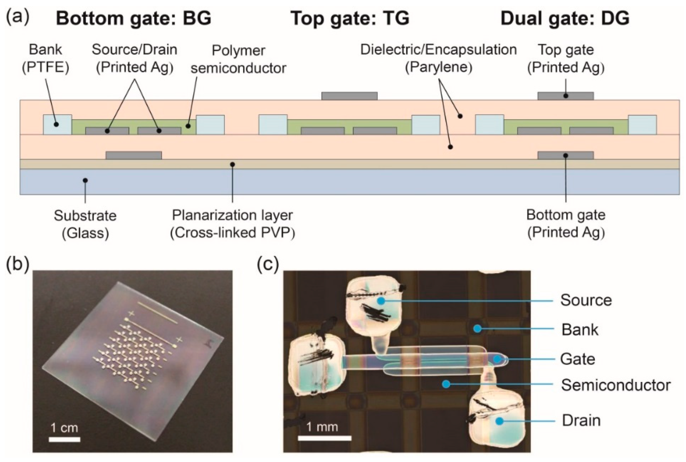
Schematic structure and photograph of the fabricated OTFT devices are shown in Figure 1. Single- and dual-gate OTFTs were integrated on a glass substrate, as shown in Figure 1a,b. Note that for the DG devices, the bottom- and top-gate electrode was connected each other. All layers except the gate dielectrics were formed by printing processes at process temperatures below 150 °C [21,22]. 140-nm-thick parylene films that were formed by chemical vapor deposition (CVD) were used as the gate dielectric and encapsulation layer. Parylene is good for low-voltage operation due to its low trap density [23] and fine thin-film formation [24]. The electrodes were fabricated by inkjet printing of a silver nanoparticle ink. Formation of the short-channels was enabled by separate printing of the source/drain electrodes as reported [25]. In this work, the standard deviation in channel length was ±2 µm. A printed fluoropolymer layer was used as a confining bank layer, whereby the semiconducting layer was printed in the area defined by the bank layer using dispenser equipment. These device fabrication processes used drop-on-demand printing techniques such as ink-jet printing and dispenser printing for ease of the layout customization.
Cross-linked poly(4-vinyl-phenol) (PVP) was formed on 0.5-mm-thick glass substrates to modify the surface wettability. PVP (MW ≈ 25,000, Sigma-Aldrich, St. Louis, MI, USA) and poly(melamine-co-formaldehyde) (MN ≈ 432.84 wt %, Sigma-Aldrich, St. Louis, MI, USA) were dissolved in propylene glycol monomethyl ether acetate (PGMEA), and spin-coated onto the substrates, followed by annealing process at 150 °C for 30 min. in ambient air to produce thermal-crosslinking. Next, a silver nanoparticle ink in hydrocarbon-based solution (NPS-JL, Harima Chemicals, Chuo-ku, Tokyo, Japan) was printed as bottom-gate electrodes using an inkjet printer (DMP2831, Fujifilm Dimatix, Santa Clara, CA, USA) with 10 pl nozzles. During the inkjet printing process, the substrates and cartridge were kept at 50 and 40 °C, respectively. The substrates were then heated at 150 °C for 15 min. in ambient air to sinter the silver nanoparticles. A 140-nm-thick parylene (diX-SR, KISCO, Tokyo, Japan) gate dielectric layer was then formed by chemical vapor deposition. Source and drain electrodes were subsequently printed in the same manner as the gate electrodes. The conditions of S/D printing and sintering process were same as those for the gate electrodes. Fluoropolymer (DuPont, Teflon AF1600) bank layers (70 nm thick) were then printed using a dispenser system (MUSASHI Engineering, Image Master 350 PC) at a pattering speed of 20 mm∙s–1 and with a discharge pressure of 6 kPa. During the dispensing process, the plates and nozzle temperatures were kept at 60 and 30 °C, respectively. A p-type donor-acceptor polymer semiconductor ink (0.03 wt %, mesitylene solvent, Mitsubishi Chemical, MOP-01) was then printed onto the area defined by the bank layer by the dispenser system at a patterning speed of 20 mm∙s−1 and discharge pressure of 2 kPa, while keeping the stage and nozzle temperatures at 60 and 30 °C, respectively, followed by an anneal at 150 °C in nitrogen globe box for 1 h to remove the solvent. 10-nm-thick semiconducting layer was obtained. Then, a 140-nm-thick parylene (diX-SR, KISCO, Tokyo, Japan) gate dielectric layer was then formed by chemical vapor deposition. Finally, top-gate electrodes were printed and sintered in the same manner as the bottom-gate electrodes.
2.2. Device Characterization
The capacitance of the dielectric was measured using an LCR meter (ZM2376, NF Corporation, Yokohama, Japan). The electrical characteristics of the OTFTs and inverter circuits were measured using a semiconductor parameter analyzer (model 4200A-SCS, Keithley, Cleveland, OH, USA). All electrical measurements were carried out in the air. Optical microscope images of the devices were obtained using a digital microscope (LEXT OLS4000, Olympus, Shinjuku, Tokyo, Japan).
2.3. Method of the Device Simulation
Device simulation in finite element method (FEM) was carried out to investigate the carrier distribution in single- and dual-gate p-type transistors by using the mathematics module of COMSOL Multiphysics (KESCO Ltd., Tokyo, Japan) [14]. The simulation was based on the Poisson equation and the continuity equation.
Here V is the electrostatic potential, e is the elementary charge, ε is the dielectric constant, nf is the free hole carrier density, nt is the trapped hole carrier density, n0 is the carrier density in the neutral state, μ is the mobility tensor, and EF is the Fermi energy. These equations contain two independent variables: V(x, y) and EF(x, y). Carrier densities nf and nt were approximated as
Here Dv is the effective density of states in the valence band, Ev is the top energy of the valence band, kB is the Boltzmann constant, T is the temperature, Dt is the total density of trap states, and Et is the average energy of traps with exponential density of states.
The parameters used in the simulation were summarized in Table 1. Channel width, channel length, channel thickness, dielectric constant of insulator (εi), and dielectric thickness were measured directly by experiments. The dielectric constant of semiconductor (εs) and temperature were set at typical values. The effective density of states in the valence band (Dv) was estimated from a typical effective mass of organic semiconductor, 3m0, and has little effect on the simulation results. Here m0 is the mass of a free electron. The other parameters, mobility, work function, ionization energy, density of trap states (Dt), average energy of trap states (Et), and carrier density in the neutral state (n0), were arbitrarily set to fit the experimental data. In the simulation, either work function or ionization energy does not matter as long as the difference between the two does not change. We assumed anisotropic mobility because it is a common nature of polymeric semiconductors as reported [26].
3. Results and Discussion
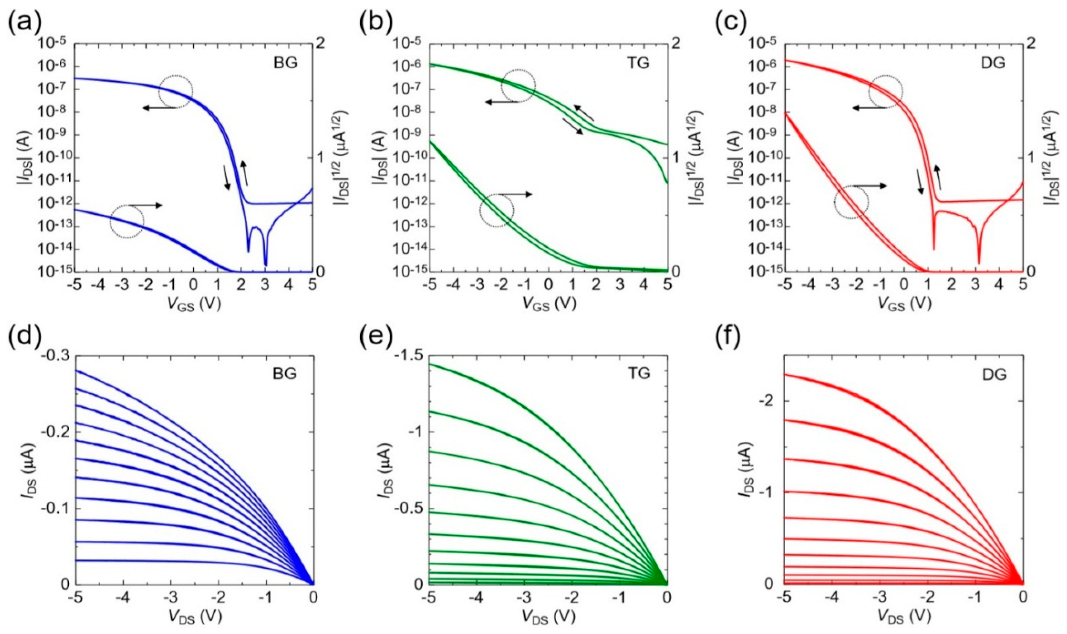
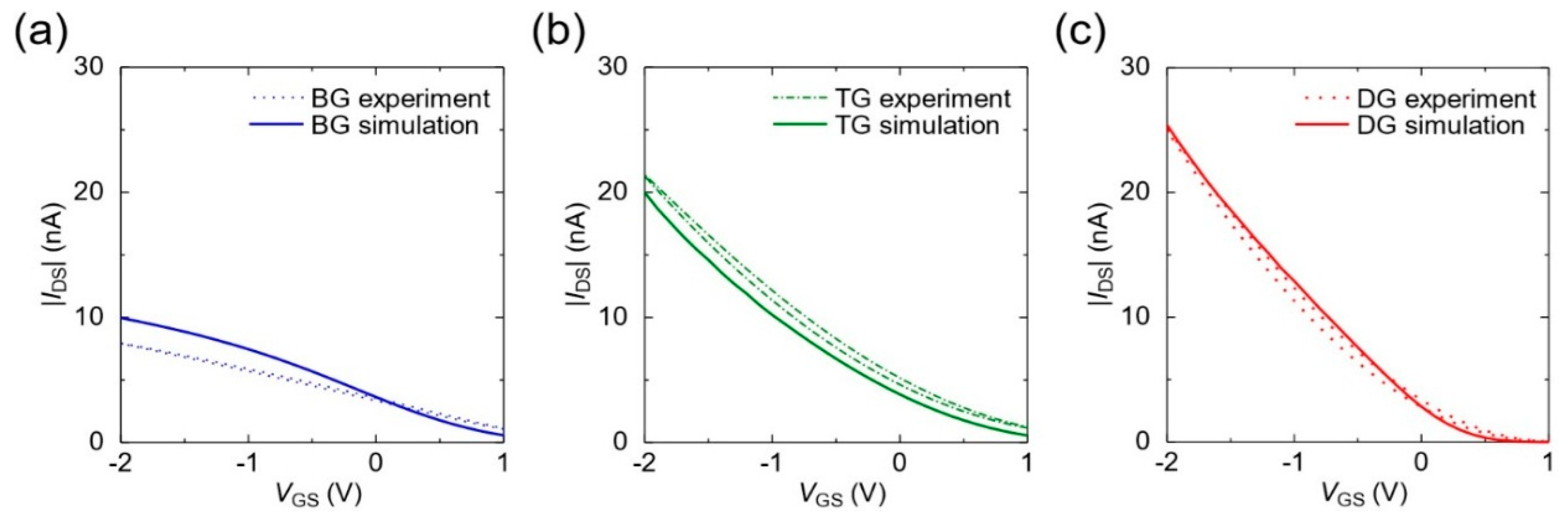
Transfer characteristics in the saturation regime and output characteristics of the OTFTs were shown in Figure 2. Transfer characteristics in the linear regime obtained from experimental and numerical simulation were shown in Figure 3. The simulated characteristics were similar to the experimental. Channel width (W) and length (L) was 740 µm and 7 µm, respectively. Capacitance per unit area was 21 nF/cm2. The electrical properties such as mobility in saturation (μsat) and linear regime (μlin), threshold voltage (VTH), on-current (ION) and subthreshold slope (SS) were summarized at Table 2. At VDS = −5 V, ION for the BG, TG, and DG devices was 0.23 ± 0.04 µA, 1.5 ± 0.2 µA, and 1.9 ± 0.2 µA, respectively. SS for the BG, TG, and DG devices was 0.5 ± 0.3 V/dec, 1.5 ± 1.0 V/dec, and 0.3 ± 0.1 V/dec, respectively. The higher ION and steeper SS were obtained: the result is consistent with that from previously reported [5,6]. Furthermore, for the DG devices, saturation (VDS = −5 V) and linear (VDS = −0.1 V) mobility was 0.05 ± 0.013 cm2/Vs and 0.047 ± 0.013 cm2/Vs, respectively. The mobility for the DG devices was also better than those of the single-gate devices. On the whole, the DG devices exhibited better electrical properties.
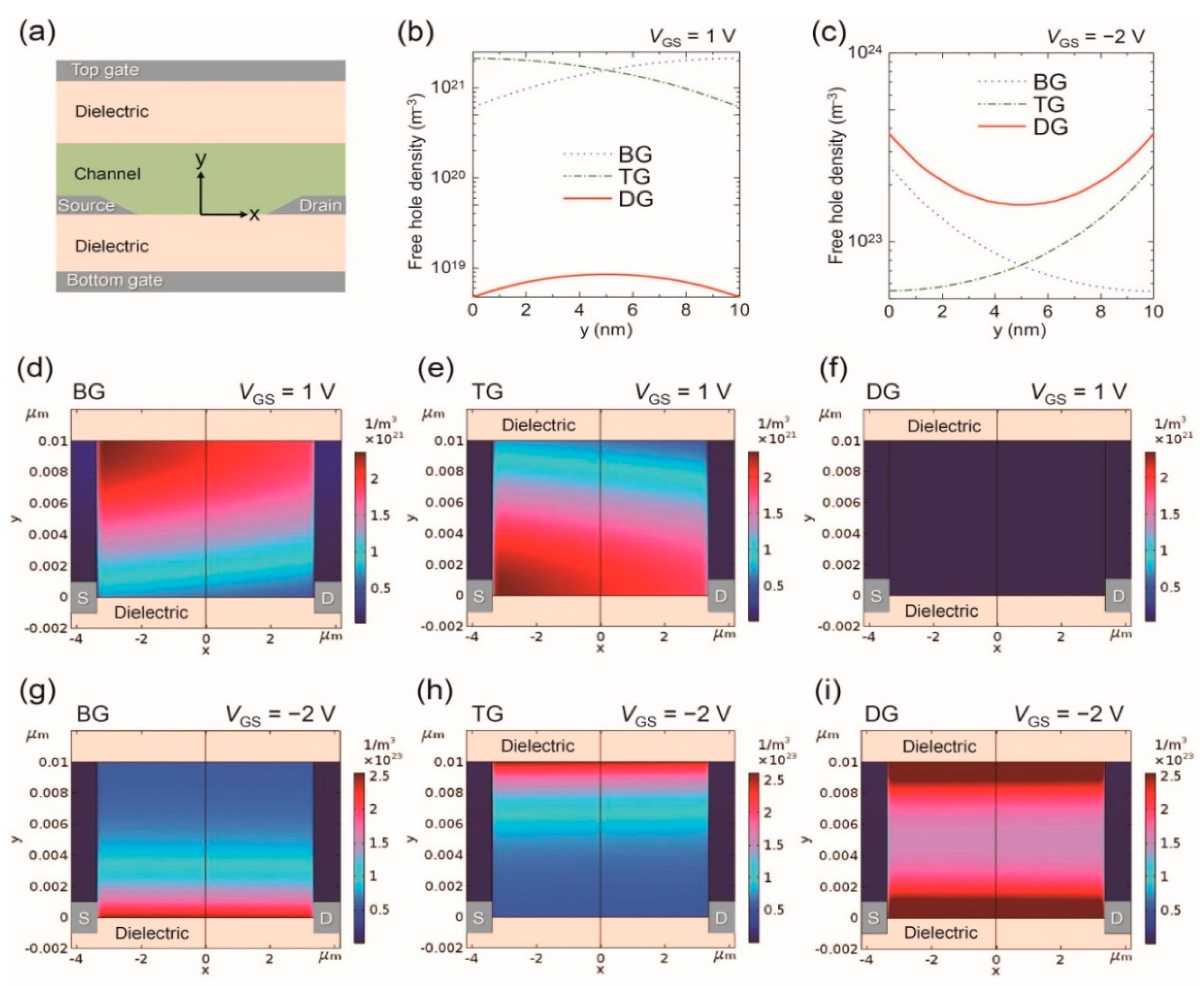
To elucidate the origin of better switching characteristics of the DG device, charge carrier distribution in the organic semiconducting layer was displayed in Figure 4. Spatial x-axis and y-axis were defined as Figure 4a, where the origin was set to be the crossing point of middle of the channel and the line along the bottom-dielectric/semiconductor interface. Free hole densities as a function of y-axis at VGS = 1 V (off state) and VGS = −2 V (on state) were shown in Figure 4b,c. VDS = −0.1 V in all three device simulations. For the single-gate devices, the carrier density at the side of the gate electrode could be controlled in the range of 6.2 × 10²⁰–2.5 × 10²³ m−3. Nevertheless, the carrier density at the opposite side of the gate electrode was hardly controlled (2.1 × 10²¹–5.5 × 10²² m−3). On the other hand, for the DG system, the carrier density over the entire region in the channel could be controlled in the wider range of 4.8 × 10¹⁸–3.8 × 10²³ m−3. This excellent control of carrier density in the DG system should contribute to obtaining the steeper SS than those from the single-gate system.
We note that the difference in threshold voltage between three device structures needs to be taken into account: however, it is well known that the determination of threshold voltage from experimental transfer characteristics is not always accurate in organic field-effect transistors [27]. On the other hand, in this simulation, the flat band gate voltages, which has a similar implication of threshold voltage, were −0.2 V for all three device structures: the comparison of carrier density at a same gate voltage is reasonable in this simulation.
Moreover, the charge carrier distributions at on/off state were visualized in Figure 4d–i. It is clear that DG device could control the carrier density well, as opposite to single-gate devices. For all the gate structure devices, the accumulation channel whose thickness was estimated to be about 2-nm-thick [28] was formed at on-state. In particular, for the DG device, the channel was formed at both bottom- and top-gate side, and carrier density of this dual-channel was estimated to be <3.8 × 10²³ m−3, which was higher density than that of single-gate devices (<2.5 × 10²³ m−3). This dual-channel obviously flow current more than the single-channel, while ION for the DG devices (IONDG) was approximately equivalent to the sum of ION for the BG devices (IONBG) and ION for the TG devices (IONTG), IONDG ≈ IONBG + IONTG, according to Table 2.
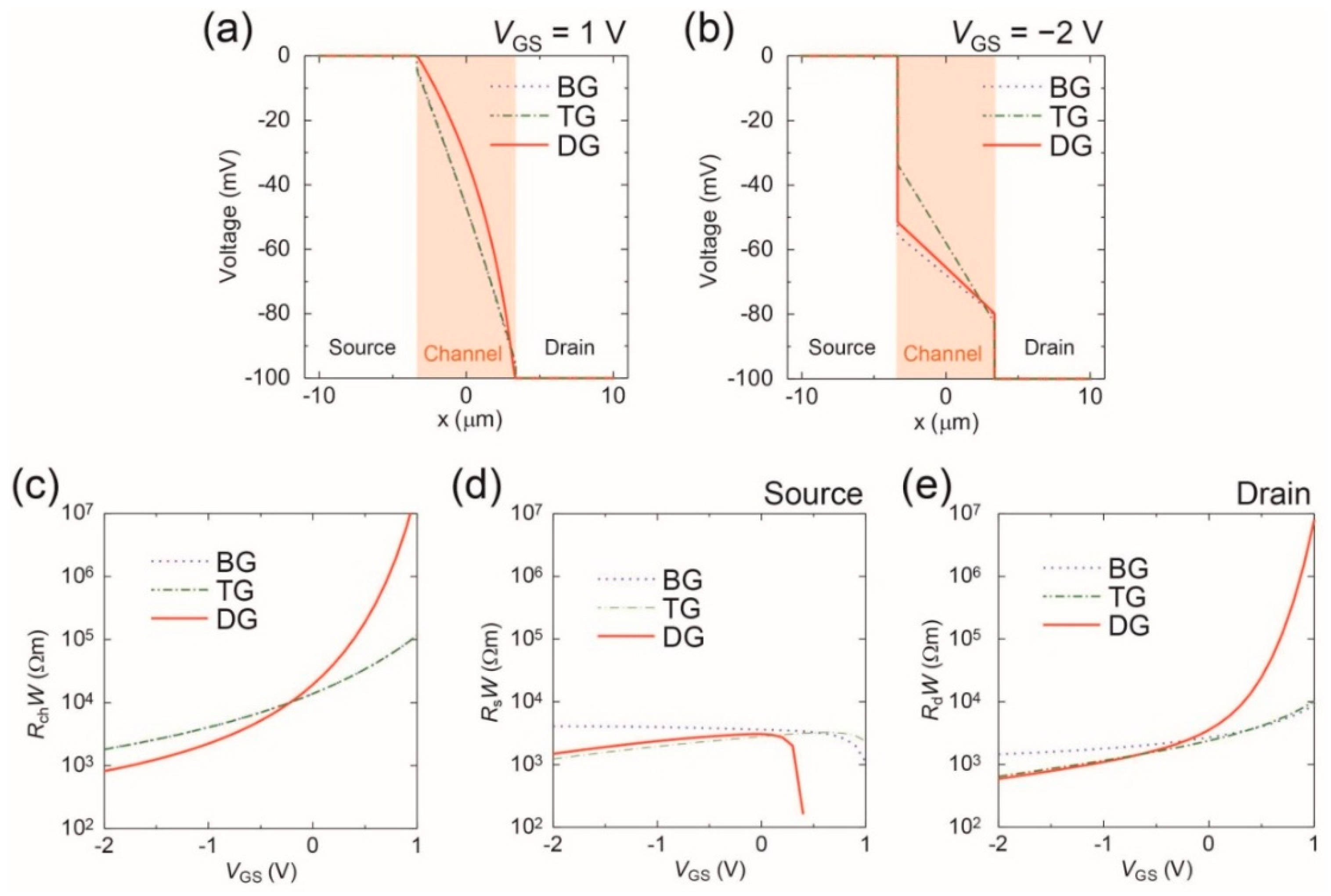
For a discussion about the reason why mobility for the DG devices was higher than that of the single-gate devices, potential in the channel were simulated, as shown in Figure 5a,b. Potential in the source and drain region was pinned at 0 V and −0.1 V, respectively. Gate voltage affected the slope of the channel potential and voltage drop at source/channel interface and channel/drain interface.
Channel-width-normalized channel resistance (RchW), contact resistance at source/channel (RsW) and channel/drain (RdW) were extracted from Figure 5a,b and plotted as a function of gate voltage in Figure 5c–e. At VGS = −2 V, RchW for the BG, TG, DG device was estimated to be 1.8 × 10³ Ωm, 1.8 × 10³ Ωm, 0.8 × 10³ Ωm, respectively. There was negligible difference between RchW for the BG device (RchWBG) and RchW for the TG device (RchWTG), on the other hand, RchW for the DG device (RchWDG) was about 55% less than that of the single-gate devices at VGS = −2 V (RchWBG ≈ RchWTG > RchWDG), because the DG device produces the dual-channel as shown in Figure 4i.
Contact resistances at VGS = −2 V for the DG device (RsWDG: 1.5 × 10³ Ωm, RdWDG: 0.6×10³ Ωm) were approximately equivalent values to those for the TG device (RsWTG: 1.2 × 10³ Ωm, RdWTG: 0.6 × 10³ Ωm). RsW and RdW (at VGS = −2 V) for the TG/DG device were 60−70% less than those for the BG device (RsWBG: 4.1 × 10³ Ωm, RdWBG: 1.5 × 10³ Ωm). In brief, RsW, RdW for the TG, DG device were less than the BG device (RsW or RdW: BG > TG ≈ DG) [29]. This is the reason why mobility for the TG, DG devices was higher than the BG devices.
Meanwhile, mobility for the DG devices was also higher than that for the TG devices. For a discussion about the reason for this, we focus on carrier density of the channels. Maximum carrier density of the dual-channel (3.8 × 10²³ m−3) was 1.5 times more than that of single-channel (2.5 × 10²³ m−3), as shown in Figure 4c. To achieve carrier density equivalent of the dual-channel, at least VGS < −2 V would be required in the TG devices. Since the mobility was associated with gate-voltage [30], we suggest that higher carrier density of the DG devices would contribute to obtaining the higher mobility than the TG devices.
4. Conclusions
In conclusion, we successfully fabricated low-voltage BG, TG, DG organic transistors by employing thin parylene dielectrics. The DG devices exhibited better switching characteristics than the single-gate devices. To elucidate this reason, charge carrier distribution and channel potential in BG, TG, DG devices were successfully simulated based on a FEM simulation. It was clear that the DG system produces a dual-channel, and that it has excellent control of charge carrier density in an organic semiconducting layer, which leads to higher ION and steeper SS than the single-gate devices. The conclusions also would apply to OTFTs that employ other organic semiconductor materials. These results can be significant information for the better understanding of a low-voltage DG device operation, as well as for the realization of the high-performance and robust organic electronics.
Author Contributions
R.S., H.M. and S.T. designed the research and experiments. T.M. prepared and supplied the polymer semiconductor material. R.S., M.T., Y.T. and T.M. performed fabrication and characterization of the organic transistors. M.T. and H.M. carried out the device simulation. Each of the authors prepared figures and helped write the manuscript.
Funding
This work was supported by the JSPS KAKENHI Grant Number 18J10982, JSPS LEADER program, JSPS KAKENHI Grant Number 18H01855, JST COI program, and JST OPERA program.
Acknowledgments
The polymer semiconductor material was provided by Mitsubishi Chemical Corporation.
Conflicts of Interest
The authors declare no conflict of interest.
References
- Someya, T.; Sekitani, T.; Iba, S.; Kato, Y.; Kawaguchi, H.; Sakurai, T. A large-area, flexible pressure sensor matrix with organic field-effect transistors for artificial skin applications. Proc. Natl. Acad. Sci. USA 2004, 101, 9966–9970. [Google Scholar] [CrossRef] [PubMed] [Green Version]
- Myny, K.; Steudel, S.; Smout, S.; Vicca, P.; Furthner, F.; van der Putten, B.; Tripathi, A.K.; Gelinck, G.H.; Genoe, J.; Dehaene, W.; et al. Organic RFID transponder chip with data rate compatible with electronic product coding. Org. Electron. 2010, 11, 1176–1179. [Google Scholar] [CrossRef]
- Wang, J.Z.; Zheng, Z.H.; Sirringhaus, H. Suppression of short-channel effects in organic thin-film transistors. Appl. Phys. Lett. 2006, 89, 083513. [Google Scholar] [CrossRef]
- Halik, M.; Klauk, H.; Zschieschang, U.; Schmid, G.; Dehm, C.; Schütz, M.; Maisch, S.; Effenberger, F.; Brunnbauer, M.; Stellacci, F. Low-voltage organic transistors with an amorphous molecular gate dielectric. Nature 2004, 431, 963–966. [Google Scholar] [CrossRef] [PubMed]
- Gelinck, G.H.; van Veenendaal, E.; Coehoorn, R. Dual-gate organic thin-film transistors. Appl. Phys. Lett. 2005, 87, 073508. [Google Scholar] [CrossRef]
- Ha, T.-J.; Sonar, P.; Dodabalapur, A. High mobility top-gate and dual-gate polymer thin-film transistors based on diketopyrrolopyrrole-naphthalene copolymer. Appl. Phys. Lett. 2011, 98, 253305. [Google Scholar] [CrossRef]
- Iba, S.; Sekitani, T.; Kato, Y.; Someya, T. Control of threshold voltage of organic field-effect transistors with double-gate structure. Appl. Phys. Lett. 2005, 87, 023509. [Google Scholar] [CrossRef]
- Hizu, K.; Sekitani, T.; Someya, T.; Otsuki, J. Reduction in operation voltage of complementary organic thin-film transistor inverter circuits using double-gate structures. Appl. Phys. Lett. 2007, 90, 093504. [Google Scholar] [CrossRef]
- Marien, H.; Steyaert, M.; van Veenendaal, E.; Heremans, P. Analog techniques for reliable organic circuit design on foil applied to an 18 dB single-stage differential amplifier. Org. Electron. 2010, 11, 1357–1362. [Google Scholar] [CrossRef]
- Marien, H.; Steyaert, M.S.J.; van Veenendaal, E.; Heremans. A Fully Integrated ΔΣ ADC in Organic Thin-Film Transistor Technology on Flexible Plastic Foil. IEEE J. Solid State Circuits 2011, 46, 276–284. [Google Scholar] [CrossRef]
- Spijkman, M.-J.; Myny, K.; Smits, E.C.P.; Heremans, P.; Blom, P.W.M.; de Leeuw, D.M. Dual-gate thin-film transistors, integrated circuits and sensors. Adv. Mater. 2011, 23, 3231–3242. [Google Scholar] [CrossRef] [PubMed]
- Myny, K.; Beenhakkers, M.J.; van Aerle, N.A.J.M.; Gelinck, G.H.; Genoe, J.; Dehaene, W.; Heremans, P. Unipolar organic transistor circuits made robust by dual-gate technology. IEEE J. Solid State Circuit 2011, 46, 1223–1230. [Google Scholar] [CrossRef]
- Marien, H.; Steyaert, M.S.J.; van Veenendaal, E.; Heremans, P. Analog building blocks for organic smart sensor systems in organic thin-film transistor technology on flexible plastic foil. IEEE J. Solid State Circuit 2012, 47, 1712–1720. [Google Scholar] [CrossRef]
- Matsui, H.; Hayasaka, K.; Takeda, Y.; Shiwaku, R.; Kwon, J.; Tokito, S. Printed 5-V organic operational amplifiers for various signal processing. Sci. Rep. 2018, 8, 8980. [Google Scholar] [CrossRef] [PubMed]
- Kumar, B.; Kaushik, B.K.; Negi, Y.S.; Goswami, V. Single and dual gate OTFT based robust organic digital design. Microelectron. Reliab. 2014, 50, 100–109. [Google Scholar] [CrossRef]
- Uemura, T.; Rolin, C.; Ke, T.-H.; Fesenko, P.; Genoe, J.; Heremans, P.; Takeya, J. On the extraction of charge carrier mobility in high-mobility organic transistors. Adv. Mater. 2016, 28, 151–155. [Google Scholar] [CrossRef] [PubMed]
- Negi, S.; Baliga, A.K.; Pandey, Y.; Mittal, P.; Kumar, B. Performance analysis of dual gate organic thin film transistor through analytical modeling. In Proceedings of the 2016 International Conference on Computing, Communication and Automation, Noida, India, 29–30 April 2016. [Google Scholar] [CrossRef]
- Takshi, A.; Dimopoulos, A.; Madden, J.D. Simulation of a dual gate organic transistor compatible with printing methods. Solid State Electron. 2008, 52, 107–114. [Google Scholar] [CrossRef]
- Xu, Y.; Darmawan, P.; Liu, C.; Li, Y.; Minari, T.; Ghibaudo, G.; Tsukagoshi, K. Tunable contact resistance in double-gate organic field-effect transistors. Org. Electron. 2012, 13, 1583–1588. [Google Scholar] [CrossRef]
- Brondijk, J.J.; Spijkman, M.; Torricelli, F.; Blom, P.W.M.; de Leeuw, D.M. Charge transport in dual-gate organic field-effect transistors. Appl. Phys. Lett. 2012, 100, 023308. [Google Scholar] [CrossRef] [Green Version]
- Kwon, J.; Takeda, Y.; Fukuda, K.; Cho, K.; Tokito, S.; Jung, S. Vertically stacked complementary organic field-effect transistors and logic circuits fabricated by inkjet printing. Adv. Electron. Mater. 2016, 2, 1600046. [Google Scholar] [CrossRef]
- Lai, S.; Cosseddu, P.; Zucca, A.; Loi, A.; Bonfiglio, A. Combining inkjet printing and chemical vapor deposition for fabrication low voltage, organic field-effect transistors on flexible substrates. Thin Solid Films 2017, 631, 124–131. [Google Scholar] [CrossRef]
- Shiwaku, R.; Matsui, H.; Hayasaka, K.; Takeda, Y.; Fukuda, T.; Kumaki, D.; Tokito, S. Printed organic inverter circuits with ultralow operating voltages. Adv. Electron. Mater. 2017, 3, 1600557. [Google Scholar] [CrossRef]
- Kondo, M.; Uemura, T.; Matsumoto, T.; Araki, T.; Yoshimoto, S.; Sekitani, T. Ultraflexible and ultrathin polymeric gate insulator for 2 V organic transistor circuits. Appl. Phys. Express 2016, 9, 061602. [Google Scholar] [CrossRef]
- Doggart, J.; Wu, Y.; Liu, P.; Zhu, S. Facile inkjet-printing self-aligned electrodes for organic thin-film transistor arrays with small and uniform channel length. ACS Appl. Mater. Interface 2010, 8, 2189–2192. [Google Scholar] [CrossRef]
- Salleo, A. Charge transport in polymeric transistors. Mater. Today 2007, 10, 38–45. [Google Scholar] [CrossRef]
- Choi, H.H.; Cho, K.; Frisbie, C.D.; Sirringhaus, H.; Podzorov, V. Critical assessment of charge mobility extraction in FETs. Nat. Mater. 2018, 17, 2–7. [Google Scholar] [CrossRef] [PubMed]
- Tanase, C.; Meijer, E.J.; Blom, P.W.M.; de Leeuw, D.M. Local charge carrier mobility in disordered organic field-effect transistors. Org. Electron. 2003, 4, 33–37. [Google Scholar] [CrossRef] [Green Version]
- Richards, T.J.; Sirringhaus, H. Analysis of the contact resistance in staggered, top-gate organic field-effect transistors. J. Appl. Phys. 2007, 102, 094510. [Google Scholar] [CrossRef]
- Kim, C.-H.; Bonnassieux, Y.; Horowitz, G. Charge distribution and contact resistance model for coplanar organic field-effect transistors. IEEE Trans. Electron Devices 2013, 60, 280–287. [Google Scholar] [CrossRef] [Green Version]
Figure 1.
(a) Schematic structures, (b) photograph and (c) layout of fabricated organic thin-film transistor (OTFT) devices.
Figure 1.
(a) Schematic structures, (b) photograph and (c) layout of fabricated organic thin-film transistor (OTFT) devices.

Figure 2.
Transfer characteristics of fabricated (a) bottom-gate (BG), (b) top-gate (TG), and (c) dual-gate (DG) OTFTs at VDS = −5 V. Output characteristics of fabricated (d) bottom-gate, (e) top-gate, and (f) dual-gate OTFTs. Gate-source voltages were from 0 to −5 V in −0.5 V step. The channel dimensions were W/L = 740 µm/ 7 µm.

Figure 3.
Transfer characteristics of (a) bottom-gate, (b) top-gate, and (c) dual-gate OTFTs obtained from the experimental and numerical simulation at VDS = −0.1 V. The channel dimensions were W/L = 740 µm/7 µm.
Figure 3.
Transfer characteristics of (a) bottom-gate, (b) top-gate, and (c) dual-gate OTFTs obtained from the experimental and numerical simulation at VDS = −0.1 V. The channel dimensions were W/L = 740 µm/7 µm.

Figure 4.
(a) Device geometry in the simulation; free hole density as a function of y-axis at (b) VGS = 1 V and (c) VGS = −2 V. Charge carrier distribution in (d) BG, (e) TG, (f) DG device at VGS = 1 V (off-state), and (g) BG, (h) TG, (i) DG devices at VGS = −2 V (on-state). VDS = −0.1 V.
Figure 4.
(a) Device geometry in the simulation; free hole density as a function of y-axis at (b) VGS = 1 V and (c) VGS = −2 V. Charge carrier distribution in (d) BG, (e) TG, (f) DG device at VGS = 1 V (off-state), and (g) BG, (h) TG, (i) DG devices at VGS = −2 V (on-state). VDS = −0.1 V.

Figure 5.
Simulation of the potential in source, channel, drain region as a function of x-axis at (a) VGS = 1 V and (b) VGS = −2 V. Channel-width-normalized (c) channel resistance (RchW), (d) source/channel contact resistance (RsW) and (e) channel/drain contact resistance (RdW) as a function of VGS.


Table 1.
Parameters Used in the finite element method (FEM) Simulation.
| Parameter | Value | Parameter | Value |
|---|---|---|---|
| Channel width | 732 µm | Temperature | 300 K |
| Channel length | 6.73 µm | Work function of source, drain and gate electrodes | 4.6 eV |
| Channel thickness | 10 nm | Ionization energy of semiconductor | 5.0 eV |
| Dielectric constant of insulator, εi | 3.38ε0 | The effective density of states in the valence band, Dv | 1.6 × 1020 cm−3 |
| Dielectric constant of semiconductor, εs | 4ε0 | ||
| Dielectric thickness | 140 nm | Density of trap states, Dt | 3 × 1018 cm−3 |
| Mobility along the channel, μx | 0.24 cm2/Vs | Average energy of trap states, Et | 0.15 eV |
| Mobility perpendicular to the channel, μy | 0.048 cm2/Vs | Carrier density in the neutral state, n0 | 3 × 1023 cm−3 |
Table 2.
Electrical Properties of the Fabricated OTFTs.
| Device Structure | μsat (cm2/Vs) | VTH (V) | ION (µA) | SS (V/dec) | μlin (cm2/Vs) | ION (nA) | SS (V/dec) |
|---|---|---|---|---|---|---|---|
| VDS = −5 V, VGS > −5 V | VDS = −0.1 V, VGS > −2 V | ||||||
| BG | 0.012 ± 0.002 | 1.5 ± 0.1 | 0.23 ± 0.04 | 0.5 ± 0.3 | 0.012 ± 0.002 | 6.4 ± 0.8 | 1.6 ± 0.3 |
| TG | 0.038 ± 0.005 | 0.68 ± 0.06 | 1.5 ± 0.2 | 1.4 ± 1.0 | 0.032 ± 0.003 | 19 ± 1 | 1.4 ± 0.2 |
| DG | 0.050 ± 0.013 | 0.42 ± 0.04 | 1.9 ± 0.2 | 0.3 ± 0.1 | 0.047 ± 0.011 | 24 ± 2 | 0.4 ± 0.1 |
© 2018 by the authors. Licensee MDPI, Basel, Switzerland. This article is an open access article distributed under the terms and conditions of the Creative Commons Attribution (CC BY) license (http://creativecommons.org/licenses/by/4.0/).
Share and Cite
MDPI and ACS Style
Shiwaku, R.; Tamura, M.; Matsui, H.; Takeda, Y.; Murase, T.; Tokito, S. Charge Carrier Distribution in Low-Voltage Dual-Gate Organic Thin-Film Transistors. Appl. Sci. 2018, 8, 1341. https://doi.org/10.3390/app8081341
AMA Style
Shiwaku R, Tamura M, Matsui H, Takeda Y, Murase T, Tokito S. Charge Carrier Distribution in Low-Voltage Dual-Gate Organic Thin-Film Transistors. Applied Sciences. 2018; 8(8):1341. https://doi.org/10.3390/app8081341
Chicago/Turabian StyleShiwaku, Rei, Masataka Tamura, Hiroyuki Matsui, Yasunori Takeda, Tomohide Murase, and Shizuo Tokito. 2018. "Charge Carrier Distribution in Low-Voltage Dual-Gate Organic Thin-Film Transistors" Applied Sciences 8, no. 8: 1341. https://doi.org/10.3390/app8081341
Note that from the first issue of 2016, this journal uses article numbers instead of page numbers. See further details here.