Magneto-Optical Kerr Effect Driven by Spin Accumulation on Cu, Au, and Pt


Department of Energy Science, Sungkyunkwan University, Suwon 16419, Korea
Appl. Sci. 2018, 8(8), 1378; https://doi.org/10.3390/app8081378
Submission received: 18 July 2018
/
Revised: 9 August 2018
/
Accepted: 13 August 2018
/
Published: 15 August 2018
(This article belongs to the Special Issue Optics in Spintronic Materials)
Abstract
:Featured Application
optical magnetometer.
Abstract
The magneto-optical Kerr effect (MOKE) has recently been achieved on non-ferromagnetic metals by injecting spin currents. To use the magneto-optical Kerr effect as a quantitative tool, it is crucial to study the relationship between the Kerr rotation angle and the spin accumulation on non-ferromagnets. In this work, I measure a transient magneto-optical Kerr rotation on non-ferromagnetic metals of Cu, Au, and Pt driven by an ultrafast spin current from an adjacent ferromagnetic metal. Through comparing the measured Kerr rotation and the calculated spin accumulation, I determine the conversion ratio between the Kerr rotation and the spin accumulation to be: −4 × 10⁻⁹ (real part), −2.5 × 10⁻⁸ (real part), and −3 × 10⁻⁹ (imaginary part) rad m A−1 for Cu, Au, and Pt, respectively, at a wavelength of 784 nm.
1. Introduction
The optical detection of the magnetization has been possible since the discovery of the Faraday effect and the magneto-optical Kerr effect (MOKE) [1,2]. The MOKE in particular is extensively used for ferromagnetic metals (FMs) because FMs tend to reflect light at a visible range of wavelength. The physical origin of the MOKE on FM is the net magnetization and spin–orbit coupling of FM [3]. The MOKE on non-ferromagnetic metals (NMs) has previously been studied by inducing a magnetic moment with an external magnetic field [4,5,6,7,8]. Recently, the MOKE detection on NMs, such as Cu and Au, has been achieved by injecting an ultrafast spin current from FM to NM in the FM/NM bilayers [9,10,11]. A spin current from FM to NM creates a spin accumulation on NM, and this spin accumulation in conjunction with the spin–orbit coupling of NM causes a rotation of the polarization of light upon reflection. The optical detection of the spin accumulation on NM enables the quantitative analysis of the spin transport as well as the spin conversion at a timescale of sub-picoseconds.
NMs with heavy atoms, such as Pt and W, have a strong spin–orbit coupling; thus, they may produce strong MOKE signals. In addition, heavy metals can generate a spin current without the use of FM. The spin Hall effect in heavy metals converts a charge current to a transverse spin current, which leads to a spin accumulation on the surfaces of the heavy metal [12,13,14]. Several groups have investigated the direct detection of the spin accumulation on heavy metals driven by the spin Hall effect using the MOKE [15,16,17]. The authors of Refs. [15,16] reported that the thermal signal driven by Joule heating dominates the optical detection and that the spin signal is absent. On the other hand, the authors of Ref. [17] reported the MOKE detection of spins on Pt and W. These conflicting reports are mainly due to the fact that the spin accumulation driven by the spin Hall effect tends to be small because of the limitation of the charge current density, the short spin relaxation time, and the small spin Hall angles of the heavy metals [12,13,14].
In this work, I generate an intense spin current from FM to NM in the FM/NM bilayers, where FM is a [Co/Ni] multilayer and NM is a Cu, Cu/Au, or Cu/Pt layer, by injecting a pulsed light to FM. FM absorbs the energy of light and generates spin currents by the ultrafast demagnetization and the spin-dependent Seebeck effect (SDSE) [9,18] (Figure 1). The spin current from FM to NM induces a spin accumulation on NM, whose peak can be as high as 103 A m−1, i.e., 1026 μB m−3, where μB is the Bohr magneton (Figure 1). I measure transient MOKE signals on Cu, Cu/Au, and Cu/Pt structures, and find that an Au or Pt layer on top of Cu significantly affects the MOKE signal. Comparing the measured MOKE data and the calculated spin accumulation, I determine the ratio between Kerr rotation (Δθ + iΔε) and spin accumulation (ΔM). The Δθ/ΔM values are −4 × 10⁻⁹ and −2.5 × 10⁻⁸ rad m A−1 for Cu and Au, respectively, and the Δε/ΔM value is −3×10⁻⁹ rad m A−1 for Pt at a wavelength of 784 nm.
2. Materials and Methods
The sample stacks consist of sap/Pt (10 nm)/FM (3.8 nm)/Cu (100 nm)/cap, where sap is a sapphire substrate with a (0001) orientation, FM is a ferromagnetic layer of [Co (0.2 nm)/Ni (0.4 nm)]×6/Co (0.2 nm), cap is a capping layer of MgO (3 nm), Au (10 nm), or Pt (2 nm). The 10 nm-thick Pt layer serves as a buffer layer for [Co/Ni]. For the perpendicular magnetic anisotropy of the Co-based multilayers, such as [Co/Pt], [Co/Pd], and [Co/Ni], a [111] textured buffer layer, such as Au, Pt, and Pd, is required with a sufficient thickness because the magnetic properties of the Co-based multilayers depend on the texture [19,20]. Without the Pt buffer layer, the [Co/Ni] multilayer has an in-plane magnetic anisotropy. The [Co/Ni] thickness is chosen to be larger than the spin diffusion length of it and to have a full remnant magnetization. It is known that a thickness of a few tens of nm of the Co-based multilayer leads to a low remnant magnetization [20]. The Cu layer is selected for NM because of its large spin diffusion length. The Cu thickness more than 100 nm is required to suppress the MOKE signal from FM when measured on the Cu side of the samples. The MOKE signal through the Cu layer attenuates with exp(−4πκd/λ), where κ is the imaginary part of the refractive index of Cu, d is the thickness of Cu, and λ is the wavelength of light. With κ of 5.6, d of 100 nm, and λ of 784 nm, the attenuation is around 10−4. When the MOKE is measured on the Cu side, the demagnetization signal dominates over the spin accumulation signal at the Cu thickness of less than 60 nm [18]. From the extrapolation of the demagnetization data of the Cu thickness 10–60 nm, the demagnetization signal through the Cu 100 nm is estimated to be <0.1 μrad [18]. The MgO layer protects the Cu layer from oxidation. The additional 1 nm-thick Ta layer, which fully oxidizes after exposure to air, is deposited on top of MgO in order to secure the passivation of MgO. Adding a thin Ta layer on top of MgO is a simple method for improving the long-term stability of the passivation of MgO, and the MgO/Ta capping layer is often used when MgO is the only oxide target inside the sputtering chamber [21]. The high uniformity of Ta on top of MgO has been verified through tunneling electron microscopy in the literature [21]. I select the Ta thickness of 1 nm by comparing the static MOKE signal of the Co (3 nm)/MgO (3 nm)/Ta (0, 1, 2 nm) structure. Ta 1 nm does not reduce the static MOKE signal, but Ta 2 nm reduces the static MOKE signal by 20%. When the Ta thickness is too thick, it does not fully oxidize, and a non-oxidized Ta layer reduces the MOKE signal. The Au and Pt layers are inert in the air, thus, the passivation layer is not necessary. Considering the spin diffusion length of Pt of a few nm, I choose the Pt thickness of 2 nm. All samples are prepared through magnetron sputtering at a base pressure of <5 × 10⁻⁸ Torr.
I measure the demagnetization of FM and the spin accumulation on NM using a time-resolved polar MOKE. The MOKE signal is collected by a balanced detector (Thorlabs, Newton, NJ, US) in conjunction with a lock-in amplifier (Stanford Research Systems, Sunnyvale, CA, US). All MOKE data are obtained by taking the difference of +z and –z directions of the magnetization of FM in order to reject any residual signal caused by a slight misalignment of the balanced detector. The noise level of the MOKE detection is around 10−8 rad. In order to quantify SDSE, I measure the temperature evolution of NM using a time-domain thermoreflectance (TDTR) with a normal photodetector (Thorlabs, Newton, NJ, US). The pump light is incident on the sap side of samples with an incident fluence of 11 J m−2. The probe light is incident on either the sap side in order to detect the demagnetization of FM, or on the cap side in order to detect the spin accumulation on Cu, Au, or Pt. The center wavelengths of the pump and probe pulses are 784 nm, and the temporal full-widths at half-maximum are ≈1 and ≈0.2 ps for the pump and probe, respectively (Coherent, Santa Clara, CA, US). I modulate pump at 10 MHz using an electro-optic modulator (Conoptics, Danbury, CT, US) and probe at 200 Hz using an optical chopper (Stanford Research Systems, Sunnyvale, CA, US.) All measurements are carried out at room temperature.
3. Results
I create a transient spin current from FM to NM by depositing a photon energy on FM. Around 30% of the pump fluence is absorbed by the samples, and the electrons of FM are thermally excited. The heat transfer from the electrons of FM to the magnons of FM leads to the bulk spin generation on the electrons of FM through ultrafast demagnetization [9],
where M is the magnetization of FM. I obtain dM/dt from the time derivative of the ultrafast demagnetization data measured with the probe on the sap side of the samples (Figure 2a,b). In order to convert the unit of the Kerr rotation (rad) to the unit of magnetization (A m−1), the Kerr rotation from the ultrafast demagnetization is divided by the static Kerr rotation of −440 μrad of the full magnetization, then multiplied by the saturation magnetization of 6 × 10⁵ A m−1. Note that although the sign of the Δθ from the ultrafast demagnetization of FM is positive, I plot the demagnetization signal to be negative in Figure 2a by adding a negative sign on the y-axis. This is because it is conventional to draw the demagnetization data as negative. The heat transfer from the electrons of FM to the electrons of NM leads to the interfacial spin generation at the FM/NM interface by the SDSE [18],
where e is the elementary charge, Ss is the effective spin-dependent Seebeck coefficient of −12 μV K−1 for [Co/Ni], L is the Lorenz number of 2.45 × 10⁸ W Ω K−2, and Jq is the electronic heat current at the FM/NM interface [18]. I obtain Jq at the FM/Cu interface by analyzing the temperature evolution of the Cu surface with a thermal conductivity of 300 W m−1 K−1 and an electron–phonon coupling of 7 × 10¹⁶ W m−3 K−1 of Cu [18] (Figure 2c,d).
Next, I measure the Kerr rotation on the NM side, where NM is Cu, Cu/Au, or Cu/Pt. In addition to the real part, an imaginary part of the MOKE is measured by inserting a quarter wave plate in the probe path. The Cu/Au layer produces about 2.3 times larger of a MOKE signal than does the Cu layer (Figure 3a,b). In both the Cu and Cu/Au layers, the real part of the MOKE is dominant, and the imaginary part is about thirty times smaller than the real part. The Pt capping layer suppresses the real part of the MOKE while it enhances the imaginary part (Figure 3c).
I calculate the spin accumulation on Cu, Au, and Pt by performing spin diffusion modeling. Generated spins on FM by gs and Gs induce diffusive spin currents to NM,
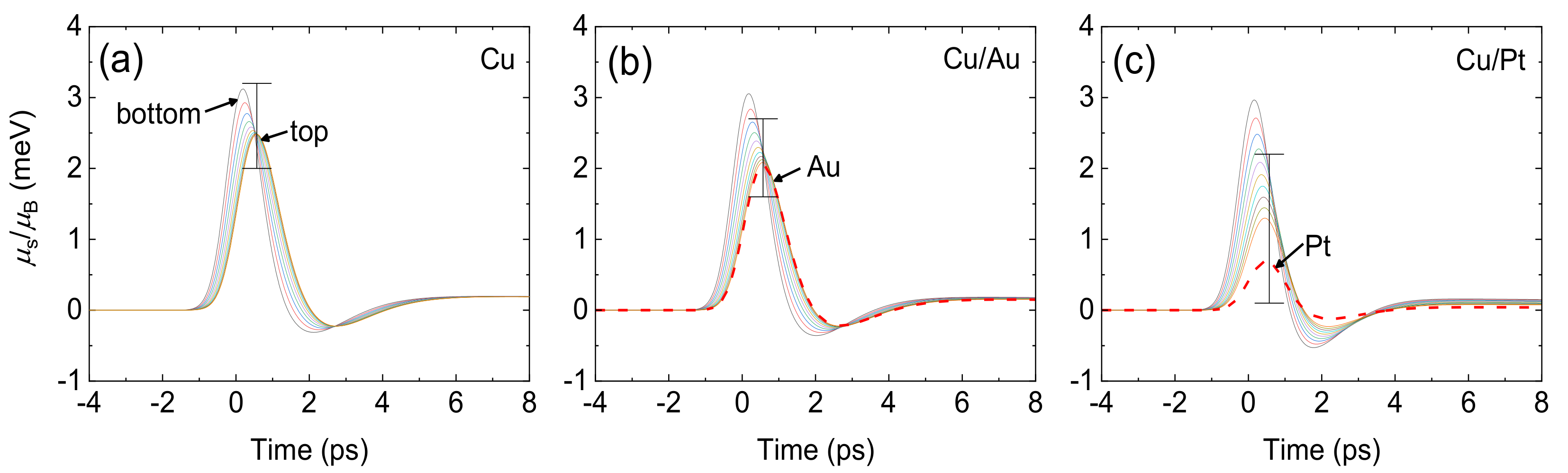
where µs is the spin chemical potential, D is the spin diffusion constant, τs is the spin relaxation time, and Ns is the spin density of states (, where NF is the electronic density of states at the Fermi level, ), with γ being the electronic heat capacity coefficient). D is calculated as , where σ is the electrical conductivity. τs is calculated as , where ls is the spin diffusion length. The µs of each layer are connected at the interface with the interfacial spin conductance , where G is the electrical conductance at the interface. I summarize the Ns, D, and τs of each layer in Table 1, and the G of each interface in Table 2 [18,22,23,24,25,26,27,28,29,30]. As spins diffuse from the bottom (the FM/Cu interface) to the surface, the time of the peak of µs shifts through the Cu thickness (Figure 4). The magnitude of µs slightly decreases through the thickness in the Cu and Cu/Au samples, and it decreases more rapidly through the thickness in the Cu/Pt sample because of the short τs of Pt (Figure 4).
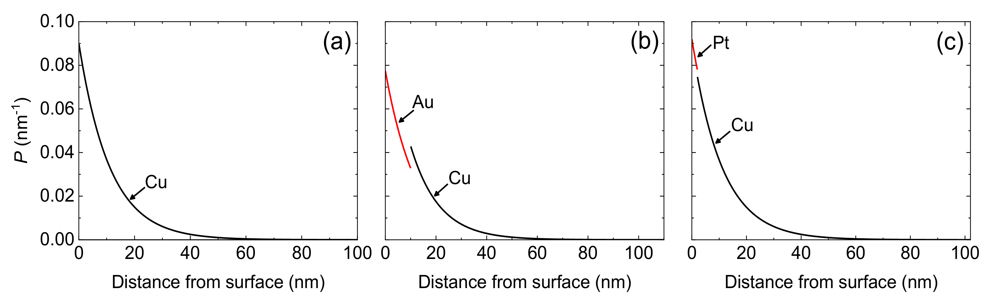
The spin accumulations on Cu, Au, and Pt contribute to the MOKE in different amounts. I calculate each layer’s relative contribution, P, to the MOKE through the thickness using a transfer matrix method with refractive indexes of 0.3 + i5.6, 0.2 + i4.9, and 2.7 + i5.9 for Cu, Au, and Pt, respectively [18] (Figure 5). The P is a fractional value, and the integration of P over the entire thickness of the capping (Au or Pt) and Cu layers is one. Using the thickness-dependent information of µs and P, the Kerr rotation can be calculated as
where d is the thickness of each layer and subscript 1 and 2 indicate the capping (Au or Pt) and Cu layer, respectively.
From the real part of the Kerr rotation of Figure 3a,b, I determine the Δθ/ΔM values to be −4 × 10⁻⁹ and −2.5 × 10⁻⁸ rad m A−1 for Cu and Au, respectively. The Δθ/ΔM value of −4 × 10⁻⁹ rad m A−1 for Cu is consistent with a previous report from Ref. [18] that used the nearly the same film structure. The six times larger Δθ/ΔM value for Au can be explained by a much larger spin–orbit coupling of Au [10]. From the imaginary part of the Kerr rotation of Figure 3c, I determine the Δε/ΔM of Pt. In this case, I assume that the imaginary part of the Kerr rotation mostly originates from Pt and thus ignore the contribution from Cu, because the imaginary part of the Kerr rotation on Cu is about thirty times smaller than the real part. The determined Δε/ΔM value is −3 × 10⁻⁹ rad m A−1 for Pt. Recently, a theory calculated the Δε for Pt to be −30 μrad at a spin accumulation of 0.02 μB per atom [17]. With an atom density of 6.6 × 1028 m−3 of Pt, the Δε/ΔM value becomes −2.4 × 10⁻⁹ rad m A−1, which is similar to our result. The Δθ/ΔM of Pt is more difficult to estimate because the Δθ data of the Cu/Pt sample have contributions from the ΔM of both Cu and Pt. In addition, the Δθ from the demagnetization of FM can have a significant contribution to the measured Δθ data when the Δθ from the spin accumulation of NM is too small. I expect that a small negative offset of the real part of the MOKE data of Figure 3c at 8 ps originates from the demagnetization signal of [Co/Ni]. The imaginary part of the MOKE data of Figure 3c shows a negligible offset because the imaginary part of the Kerr rotation of [Co/Ni] is smaller than the real part by an order of magnitude [31,32].
4. Discussion
The uncertainties of the
/ΔM mostly originate from the calculation of the spin accumulation in Figure 4. In the modeling of Figure 4, the non-thermal processes are not considered. It has been reported that hot electrons that are far above the Fermi level can amplify the spin transport from FM to NM via so-called non-thermal SDSE [33]. For an approximate estimation of the effect of the hot electrons, I calculate the spin accumulation on NM with two times smaller/larger Gs of the Equation (2). The variation of the spin accumulation on Cu and Au is less than 30%. Another source for the uncertainty is the spin diffusion length, ls, of NM. For Cu and Au, the uncertainty of ls is not important because the thicknesses of Cu and Au are much smaller than ls of Cu and Au. However, ls of Pt critically affects the spin accumulation. In the modeling of Figure 4, I use 4 nm for the ls of Pt considering the linear relationship between ls and electrical conductivity, which is 6.6 × 10⁶ Ω−1 m−1 in our sample [23]. Allowing for the variation of ls of Pt from 1.4 to 11 nm [17,23,34], the uncertainty of the spin accumulation on Pt is more than 300%, and the Δε/ΔM value ranges from −1 × 10⁻⁹ rad m A−1 at ls of 11 nm to −2.1 × 10⁻⁸ rad m A−1 at ls of 1.4 nm. Further research into the dependence on thickness of the spin accumulation is required in order to clearly reveal the effect of ls and narrow the uncertainty of the /ΔM.
The time-resolved optical detection of spins on NM can be used to investigate the spin transport and spin conversion in various NM materials. For a quantitative analysis of the spin transport and conversion, the relationship between the spin accumulation and the Kerr rotation of a variety of NM materials should be studied.
Author Contributions
All works including sample fabrication, optical detection, analysis, and writing manuscript are done by G.M. Choi.
Funding
This work is supported by the Basic Science Research Program through the National Research Foundation of Korea (NRF) funded by the Ministry of Science, ICT & Future Planning (2018R1C1B5041975).
Acknowledgments
No acknowledgment.
Conflicts of Interest
The authors declare no conflict of interest.
References
- Faraday, M. Experimental researches in electricity.—Nineteenth series. Philos. Trans. R. Soc. Lond. 1846, 136, 1–20. [Google Scholar] [CrossRef]
- Kerr, J. On rotation of the plane of polarization by reflection from the pole of a magnet. Philos. Mag. J. Sci. 1877, 3, 321–343. [Google Scholar] [CrossRef]
- Ebert, H. Magneto-optical effects in transition metal systems. Rep. Prog. Phys. 1996, 59, 1665–1735. [Google Scholar] [CrossRef]
- Stern, E.A.; McGgroddy, J.C.; Harte, W.E. Polar refection Faraday effect in metals. Phys. Rev. 1964, 135, A1306–A1314. [Google Scholar] [CrossRef]
- McGgroddy, J.C.; McAlister, A.J.; Stern, E.A. Polar refection Faraday effect in silver and gold. Phys. Rev. 1965, 139, A1844–A1848. [Google Scholar] [CrossRef]
- Schnatterly, S.E. Magetoreflection measurements on the noble metals. Phys. Rev. 1969, 183, 664–667. [Google Scholar] [CrossRef]
- Uba, L.; Uba, S.; Antonov, V.N. Magneto-optical Kerr spectroscopy of platinum. Phys. Rev. B 2000, 62, 16510–16521. [Google Scholar] [CrossRef]
- Uba, L.; Uba, S.; Antonov, V.N. Magneto-optical Kerr spectroscopy of noble metals. Phys. Rev. B 2017, 96, 235132. [Google Scholar] [CrossRef]
- Choi, G.M.; Min, B.C.; Lee, K.J.; Cahill, D.G. Spin current generated by thermally driven ultrafast demagnetization. Nat. Commun. 2014, 5. [Google Scholar] [CrossRef] [PubMed]
- Choi, G.M.; Cahill, D.G. Kerr rotation in Cu, Ag, and Au driven by spin accumulation and spin-orbit coupling. Phys. Rev. B 2014, 90, 214432. [Google Scholar] [CrossRef]
- Hofherr, M.; Maldonado, P.; Schmitt, O.; Berritta, M.; Bierbrauer, U.; Sadashivaiah, S.; Schellekens, A.J.; Koopmans, B.; Steil, D.; Cinchetti, M.; et al. Speed and efficiency of femtosecond spin current injection into a nonmagnetic material. Phys. Rev. B 2017, 96, 100403. [Google Scholar] [CrossRef]
- Dyakonov, M.I.; Perel, V.I. Possibility of orienting electron spins with current. JETP Lett. 1971, 13, 657–660. [Google Scholar]
- Hirsch, J.E. Spin Hall effect. Phys. Rev. Lett. 1999, 83, 1834–1837. [Google Scholar] [CrossRef]
- Sinova, J.; Valenzuela, S.O.; Wunderlich, J.; Back, C.H.; Jungwirth, T. Spin Hall effects. Rev. Mod. Phys. 2015, 87, 1213–1259. [Google Scholar] [CrossRef]
- Riego, P.; Vélez, S.; Gomez-Perez, J.M.; Arregi, J.A.; Hueso, L.E.; Casanova, F.; Berger, A. Absence of detectable current-induced magneto-optical Kerr effects in Pt, Ta, and W. Appl. Phys. Lett. 2016, 109, 17402. [Google Scholar] [CrossRef]
- Su, Y.; Wang, H.; Li, J.; Tian, C.; Wu, R.; Jin, X.; Shen, Y.R. Absence of detectable MOKE signals from spin Hall effect in metals. Appl. Phys. Lett. 2016, 109. [Google Scholar] [CrossRef]
- Stamm, C.; Murer, C.; Berritta, M.; Feng, J.; Gabureac, M.; Oppeneer, P.M.; Gambardell, P. Magneto-optical detection of the spin Hall effect in Pt and W thin films. Phys. Rev. Lett. 2017, 119, 087203. [Google Scholar] [CrossRef]
- Choi, G.M.; Moon, C.H.; Min, B.C.; Lee, K.J.; Cahill, D.G. Thermal spin-transfer torque driven by the spin-dependent Seebeck effect in metallic spin-valves. Nat. Phys. 2015, 11, 576–581. [Google Scholar] [CrossRef]
- Daalderop, G.H.O.; Kelly, P.J.; Broeder, F.J.A. Prediction and confirmation of perpendicular magnetic anisotropy in Co/Ni multilayers. Phys. Rev. Lett. 1992, 68, 682–685. [Google Scholar] [CrossRef] [PubMed]
- You, L.; Sousa, R.C.; Rodmacq, B.; Dieny, B. Co/Ni multilayers with perpendicular anisotropy for spintronic device applications. Appl. Phys. Lett. 2012, 100, 172411. [Google Scholar] [CrossRef]
- Gweon, H.K.; Yun, S.J.; Lim, S.H. A very large perpendicular magnetic anisotropy in Pt/Co/MgO trilayers fabricated by controlling the MgO sputtering power and its thickness. Sci. Rep. 2018, 8, 1–8. [Google Scholar] [CrossRef] [PubMed]
- Tari, A. The Specific Heat of Matter at Low Temperatures; Imperial College Press: London, UK, 2003; ISBN 978-1-86094-314-0. [Google Scholar]
- Sagasta, E.; Omori, Y.; Isasa, M.; Gradhand, M.; Hueso, L.E.; Niimi, Y.; Otani, Y.C.; Casanova, F. Tuning the spin Hall effect of Pt from the moderately dirty to the superclean regime. Phys. Rev. B 2016, 94, 060412. [Google Scholar] [CrossRef]
- Jedema, F.J.; Nijboer, M.S.; Filip, A.T.; van Wees, B.J. Spin injection and spin accumulation in all-metal mesoscopic spin valves. Phys. Rev. B 2003, 67, 085319. [Google Scholar] [CrossRef]
- Kimura, T.; Sato, T.; Otani, Y. Estimation of spin-diffusion length from the magnitude of spin-current absorption: Multiterminal ferromagnetic/nonferromagnetic hybrid structures. Phys. Rev. B 2005, 72, 014461. [Google Scholar] [CrossRef]
- Sharma, A.; Romero, J.A.; Theodoropoulou, N.; Loloee, R.; Pratt, W.P., Jr.; Bass, J. Specific resistance and scattering asymmetry of Py/Pd, Fe/V, Fe/Nb, and Co/Pt interfaces. J. Appl. Phys. 2007, 102, 113916. [Google Scholar] [CrossRef]
- Bass, J.; Pratt, W.P., Jr. Current-perpendicular (CPP) magnetoresistance in magnetic metallic multilayers. J. Magn. Magn. Mater. 1999, 200, 274–289. [Google Scholar] [CrossRef]
- Moreau, C.E.; Moraru, I.C.; Birge, N.O.; Pratt, W.P., Jr. Measurement of spin diffusion length in sputtered Ni films using a special exchange-biased spin valve geometry. Appl. Phys. Lett. 2007, 90. [Google Scholar] [CrossRef]
- Henry, L.L.; Yang, Q.; Holody, P.; Loloee, R.; Pratt Jr., W.P.; Bass, J. Perpendicular interface resistances in sputtered Ag/Cu, Ag/Au, and Au/Cu multilayers. Phys. Rev. B 1996, 54, 12336–12341. [Google Scholar] [CrossRef]
- Kurt, H.; Loloee, R.; Eid, K.; Pratt, W.P., Jr.; Bass, J. Spin-memory loss at 4.2 K in sputtered Pd and Pt and at Pd/Cu and Pt/Cu interfaces. Appl. Phys. Lett. 2002, 81, 4787–4789. [Google Scholar] [CrossRef]
- Weller, D.; Harp, G.R.; Farrow, R.F.C.; Cebollad, A.; Sticht, J. Orientation dependence of the polar Kerr effect in fcc and hcp Co. Phys. Rev. Lett. 1994, 72, 2097–2100. [Google Scholar] [CrossRef] [PubMed]
- Visnovsky, S.; Parizek, V.; Nyvlt, M.; Kiela, P.; Prosser, V.; Krishnan, R. Magneto-optical Kerr spectra of nickel. J. Magn. Magn. Mater. 1993, 127, 135–139. [Google Scholar] [CrossRef]
- Alekhin, A.; Razdolski, I.; Ilin, N.; Meyburg, J.P.; Diesing, D.; Roddatis, V.; Rungger, I.; Stamenova, M.; Sanvito, S.; Bovensiepen, U.; et al. Femtosecond spin current pulses generated by the nonthermal spin-dependent Seebeck effect and interaction with ferromagnets in spin valves. Phys. Rev. Lett. 2017, 119, 017202. [Google Scholar] [CrossRef] [PubMed]
- Liu, L.; Buhrman, R.A.; Ralph, D.C. Review and Analysis of Measurements of the Spin Hall Effect in Platinum. arXiv, 2011; arXiv:1111.3702. [Google Scholar]
Figure 1.
Schematic of the experiment. The sample structure is Pt/FM (ferromagnetic metal)/Cu/cap, where cap is Au or Pt. The pump energy drives the ultrafast demagnetization and the spin-dependent Seebeck effect on FM. The ultrafast demagnetization generates spins at the bulk of FM (gs), and the spin-dependent Seebeck effect generates spin at the FM/NM (non-ferromagnetic metal) interfaces (Gs). When the FM thickness is small, the spin generation at the Pt/FM interface is the negative value of that at the FM/Cu interface. The generated spins on FM diffuse to adjacent layers and induce a spin accumulation on Cu and cap (blue arrows). The spin accumulation on Cu and cap rotates the polarization of the probe upon reflection.

Figure 2.
The spin generation on FM. (a) The Kerr rotation due to the ultrafast demagnetization of FM with the probe on the sap side of the sap/Pt(10)/[Co/Ni](3.8)/Cu(100)/MgO(3) sample. The ultrafast demagnetization data is nearly identical with either Au or Pt capping on top of Cu. (b) The bulk spin generation rate on FM obtained from the time derivative of the demagnetization data of (a) (black circles). The red line is a fitting with a Gaussian function. (c) The temperature increase of the Cu surface of the sap/Pt(10)/[Co/Ni](3.8)/Cu(100)/MgO(3) sample. Black circles are data points obtained from time-domain thermoreflectance (TDTR), and the red line is the result of the thermal modeling. (d) The black line is the heat current at the FM/Cu interface estimated from the thermal modeling of (c). The red line is the interfacial spin generation rate at the FM/Cu interface obtained by the Equation (2) in the main text.
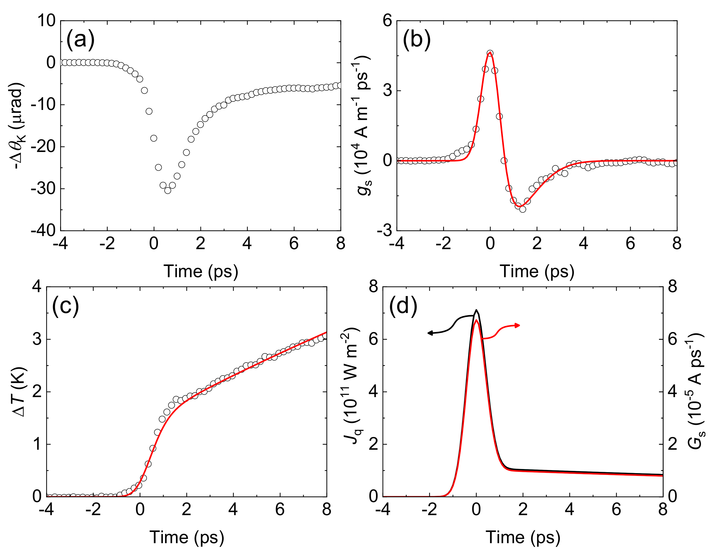
Figure 3.
Detection of the spin accumulation on NM. The Kerr rotation due to the spin accumulation on NM with the probe on the cap side of the sap/Pt(10)/[Co/Ni](3.8)/Cu(100)/cap sample, where cap is (a) MgO(3), (b) Au(10), and (c) Pt(2). Black squares and red circles are the real and imaginary parts of the Kerr rotation, respectively.
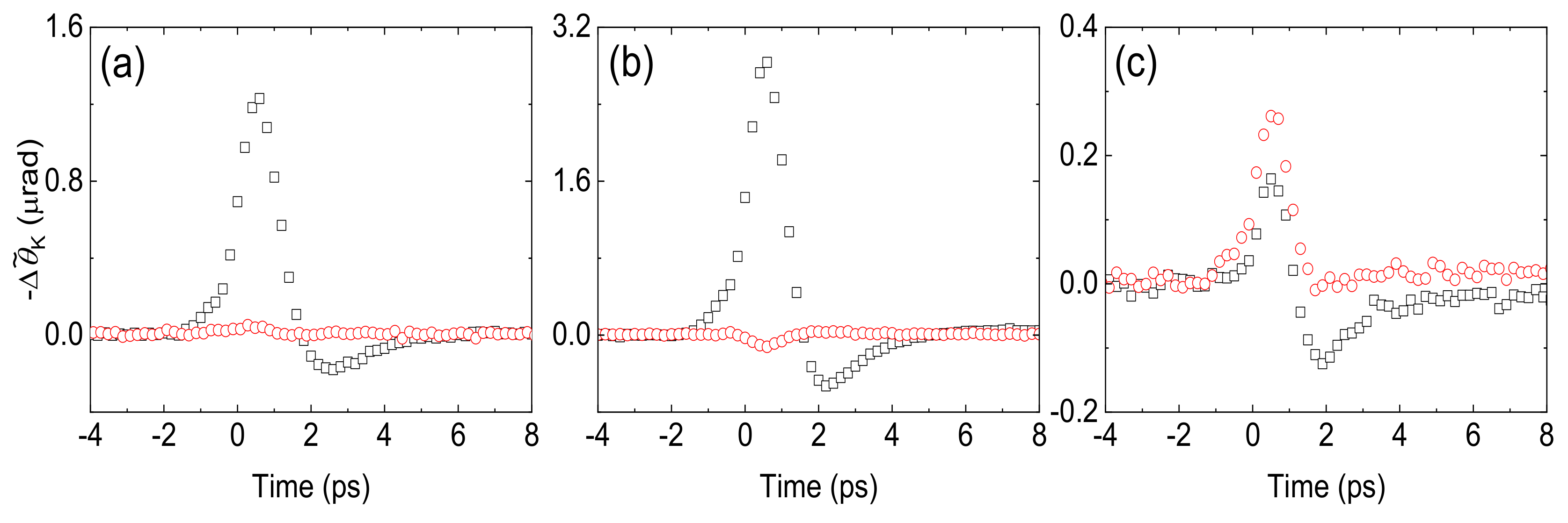
Figure 4.
Calculation of the spin accumulation on NM. Spin chemical potentials along the thickness of NM of the Pt(10)/FM(3.8)/NM structure, where NM is (a) Cu(100)/MgO(3), (b) Cu(100)/Au(10), or (c) Cu(100)/Pt(2). Solid lines represent the spin chemical potentials of Cu, and every line is an average of 10 nm thickness starting from the bottom (the FM/Cu interface) to the top surface. Red dashed lines represent the spin chemical potentials of Au (average of 10 nm thickness) in (b) and of Pt (average of 2 nm thickness) in (c).

Figure 5.
Thickness resolved magneto-optic Kerr effect (MOKE). Relative contribution to the Kerr rotation through the thickness of NM of the Pt(10)/FM(3.8)/NM structure, where NM is either (a) Cu(100), (b) Cu(100)/Au(10), or (c) Cu(100)/Pt(2). Black solid lines are the contribution from Cu, and red solid lines are the contribution from Au in (b) and from Pt in (c).

Table 1.
Bulk parameters for the spin diffusion modeling. γ is the electronic heat capacity coefficient, Ns is the spin density of states, σ is the electrical conductivity, D is the diffusion constant, ls is the spin diffusion length, and τs is the spin relaxation time.
Table 1.
Bulk parameters for the spin diffusion modeling. γ is the electronic heat capacity coefficient, Ns is the spin density of states, σ is the electrical conductivity, D is the diffusion constant, ls is the spin diffusion length, and τs is the spin relaxation time.
| Parameter | Pt | [Co/Ni] | Cu | Au |
|---|---|---|---|---|
| γ (J m−3 K−2) | 721 a | 930 b | 97 a | 97 a |
| Ns (eV−1 nm−3) | 92 | 118 | 13 | 9 |
| σ (106 Ω−1 m−1) | 6.6 c | 3 c | 39 c | 27 c |
| D (nm2 ps−1) | 220 | 80 | 9500 | 9800 |
| ls (nm) | 4 d | 2.8 e | 400 f | 60 g |
| τs (ps) | 0.07 | 0.1 | 17 | 0.4 |
Table 2.
Interfacial parameters for the spin diffusion modeling. G is the electrical conductance at the interface.
Table 2.
Interfacial parameters for the spin diffusion modeling. G is the electrical conductance at the interface.
| Parameter | Pt/[Co/Ni] | [Co/Ni]/Cu | Cu/Au | Cu/Pt |
|---|---|---|---|---|
| G (1015 Ω−1 m−2) | 1.5 a | 3 b | 6.7 c | 1.3 d |
© 2018 by the author. Licensee MDPI, Basel, Switzerland. This article is an open access article distributed under the terms and conditions of the Creative Commons Attribution (CC BY) license (http://creativecommons.org/licenses/by/4.0/).
Share and Cite
MDPI and ACS Style
Choi, G.-M. Magneto-Optical Kerr Effect Driven by Spin Accumulation on Cu, Au, and Pt. Appl. Sci. 2018, 8, 1378. https://doi.org/10.3390/app8081378
AMA Style
Choi G-M. Magneto-Optical Kerr Effect Driven by Spin Accumulation on Cu, Au, and Pt. Applied Sciences. 2018; 8(8):1378. https://doi.org/10.3390/app8081378
Chicago/Turabian StyleChoi, Gyung-Min. 2018. "Magneto-Optical Kerr Effect Driven by Spin Accumulation on Cu, Au, and Pt" Applied Sciences 8, no. 8: 1378. https://doi.org/10.3390/app8081378
Note that from the first issue of 2016, this journal uses article numbers instead of page numbers. See further details here.