Brief Report

An Al2O3 Gating Substrate for the Greater Performance of Field Effect Transistors Based on Two-Dimensional Materials

1
College of Science, National University of Defense Technology, Changsha 410073, China
2
College of Optoelectronic Science and Engineering, National University of Defense Technology, Changsha 410073, China
3
College of Physics and Electronics, Central South University, Changsha 410073, China
*
Authors to whom correspondence should be addressed.
Nanomaterials 2017, 7(10), 286; https://doi.org/10.3390/nano7100286
Submission received: 14 August 2017 / Revised: 18 September 2017 / Accepted: 18 September 2017 / Published: 22 September 2017
(This article belongs to the Special Issue Graphene and Nanotube Based Devices)

Abstract

:
We fabricated 70 nm Al2O3 gated field effect transistors based on two-dimensional (2D) materials and characterized their optical and electrical properties. Studies show that the optical contrast of monolayer graphene on an Al2O3/Si substrate is superior to that on a traditional 300 nm SiO2/Si substrate (2.4 times). Significantly, the transconductance of monolayer graphene transistors on the Al2O3/Si substrate shows an approximately 10-fold increase, due to a smaller dielectric thickness and a higher dielectric constant. Furthermore, this substrate is also suitable for other 2D materials, such as WS2, and can enhance the transconductance remarkably by 61.3 times. These results demonstrate a new and ideal substrate for the fabrication of 2D materials-based electronic logic devices.

Graphical Abstract

1. Introduction

Two-dimensional (2D) materials, such as graphene and transition-metal dischalcogenides (TMDs), have attracted tremendous interest for possible applications in transistors [1,2,3,4], photodetectors [5,6], and touch panels [7,8] owing to their extraordinary properties. However, most efforts to date employ a 300 nm thick silicon dioxide (SiO2) substrate as the gate dielectric layer. This substrate is widely used is mainly because 2D materials can be readily visualized using an optical microscope due to optical interference [9,10,11]. Although they have led to many interesting scientific discoveries [12,13,14], applying 300 nm SiO2 substrates will greatly reduce the performance of the devices, especially the signal amplification capability, which is one of the most important parameters of contemporary integrated circuits [15,16]. The devices fabricated on SiO2/Si substrates lack enough capability to regulate the Fermi surface of samples, thus requiring higher back-gate voltage [15]. Generally, the top-gate structure is adopted to enhance the gate capacitance of field effect transistors (FETs). However, its fabrication is challenging, as 2D materials lack dangling bonds [17,18]. Although many alternate approaches have been demonstrated, they inevitably result in the degradation of carrier mobility [19,20].
Previously, Liao et al. firstly reported that applying 72 nm Al2O3/Si substrates could improve the optical contrast and electrical properties of single-graphene FETs [21]. However, the Al2O3 film they fabricated was not well insulated since they directly attached tape onto the Al2O3/Si substrate using mechanical exfoliation [6]. This conventional method may damage Al2O3 films due to the strong adhesive force of the tape [21]. In our experiments, the deterministic transfer method was applied to transfer graphene onto an Al2O3/Si substrate to avoid this problem. In addition, the corrosion time of the HF solution was carefully controlled so that the wafer would be smoother, which was beneficial for forming a dense Al2O3 film via atomic layer deposition (ALD) growth. Accordingly, our single-layer graphene FETs, compared to those of Liao’s work, achieved a greater performance. Furthermore, we systematically investigated WS2 FETs on an Al2O3 gating substrate, showing that this superior substrate is also suitable for other 2D materials.

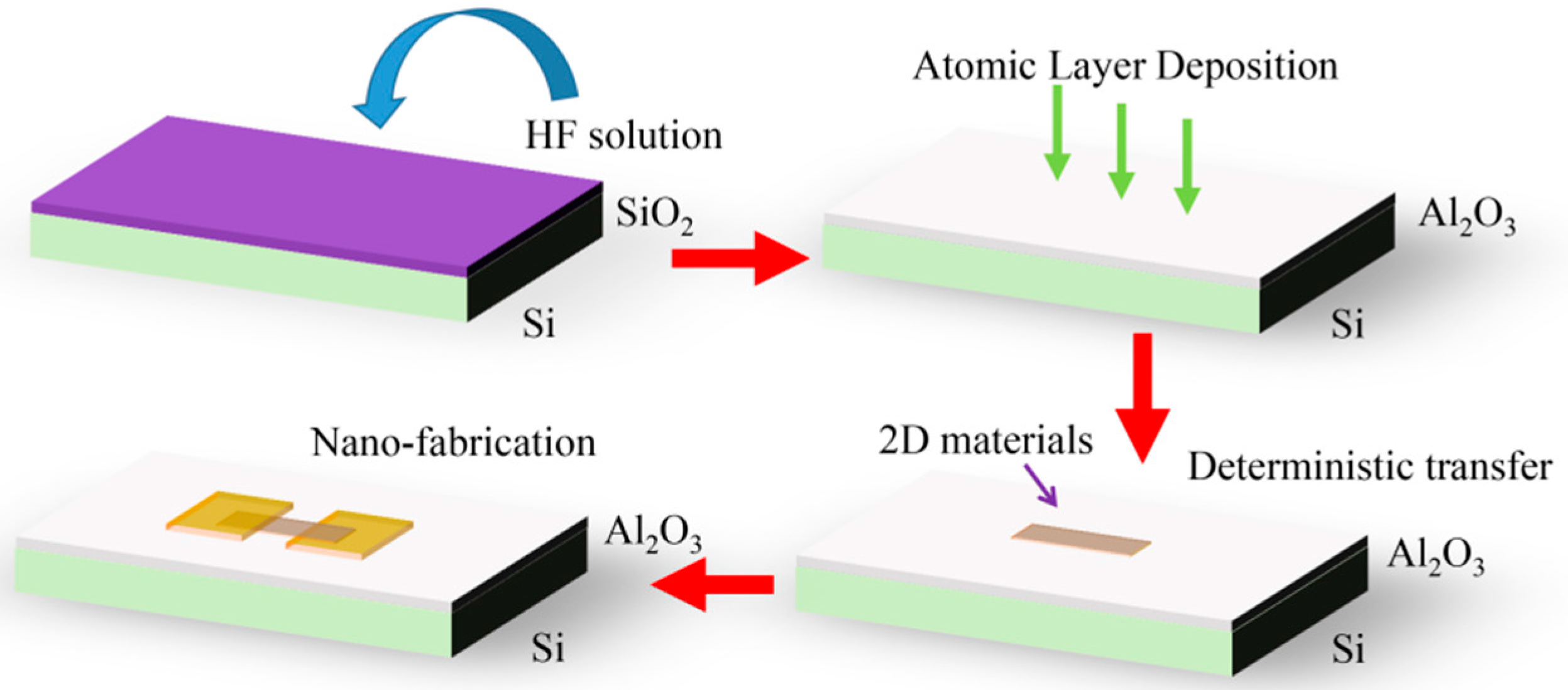
2. Experimental Details

Figure 1 illustrates the fabrication process of graphene- (or WS2)-based FETs on Al2O3/Si substrates. Firstly, an Al2O3 film was deposited on silicon (doped n++, conductivity: 0.01–0.02 Ω·cm) wafers via the ALD technique using tri-methyl-aluminum ((CH3)3Al) and distilled water as the source (reaction temperature: 250 °C). Prior to the deposition of Al2O3, a native SiO2 layer was removed with a 5% (mole ratio) hydrofluoric acid (HF) solution (40 min). After the Al2O3 film was deposited, graphene (or WS2) was transferred onto that substrate via the deterministic transfer method [22] (see Figure S1). At last, the source and drain contacts were patterned using e-beam lithography (EHT: 10 kV, aperture size: 30 μ m, beam current: 217.1 pA), and 10 nm Ti/50 nm Au were deposited using e-beam evaporation (vacuum: 1 × 10⁻⁵ Pa, evaporation rate: Ti: 0.5 Å/s; Au: 1.5 Å/s).
The topography of the samples was characterized via atomic force microscopy (AFM, NT-MDT company, Moscow, Russia, scanning mode: Semi-contact, scanning frequency: 1.01 (Hz), scanning electron microscopy (SEM, Raith company, Dortmund, Germany) and optical microscopy (Nikon company, Tokyo, Japan). The Raman and contrast spectra were recorded with Confocal Raman Spectrometer (WiTec company, Ulm, Germany, exciting laser wavelength: 532 nm, spot size: 2 μ m). The thickness of the Al2O3 film was obtained with GES-5 ellipsometer (Sopra Company, Annecy, France) and calculated to be approximately 70 nm. All characterizations were conducted in ambient conditions and at room temperature (300 K). The electrical properties were measured with 4200-SCS probe system (Keithley Company, Cleveland, OH, USA).

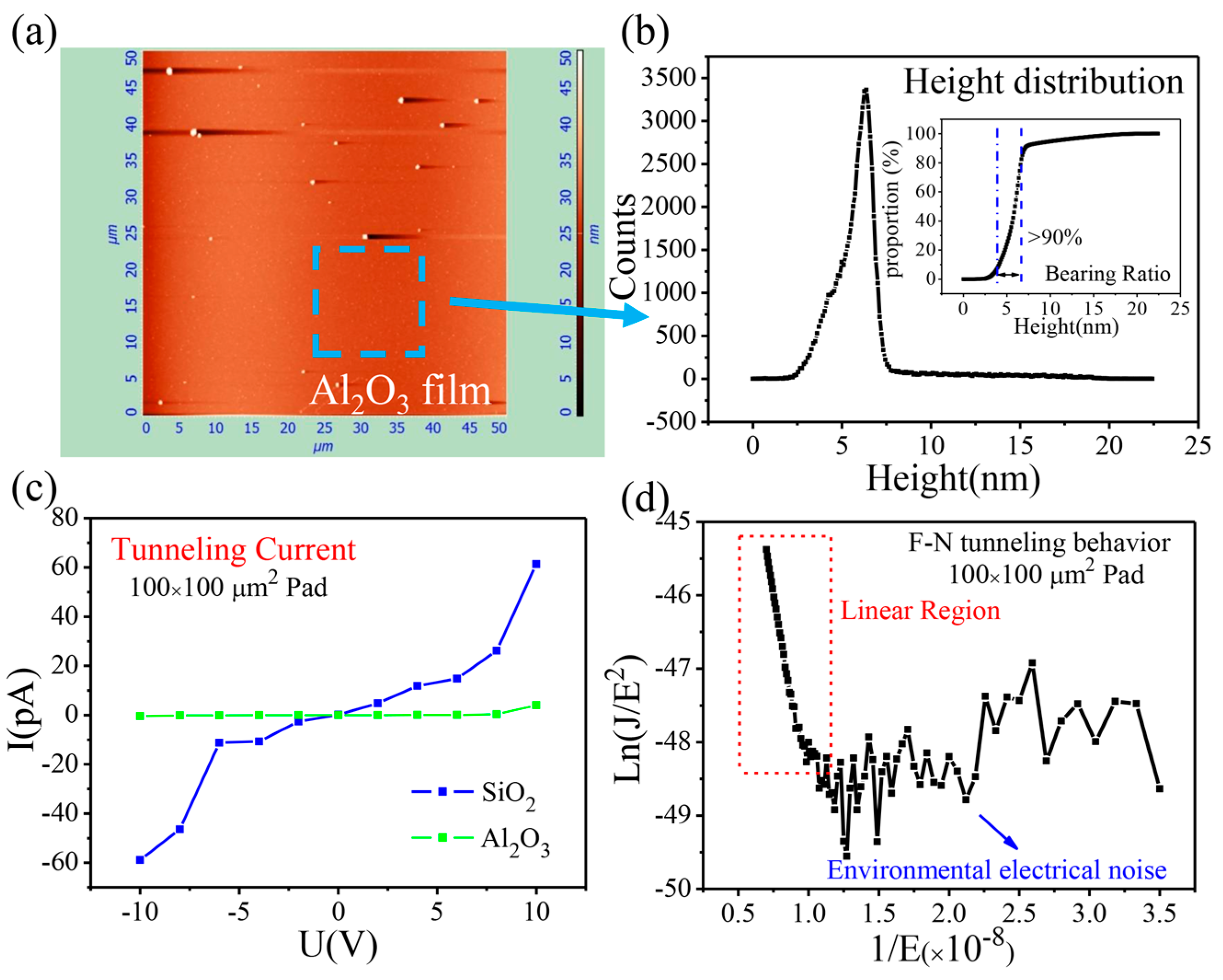
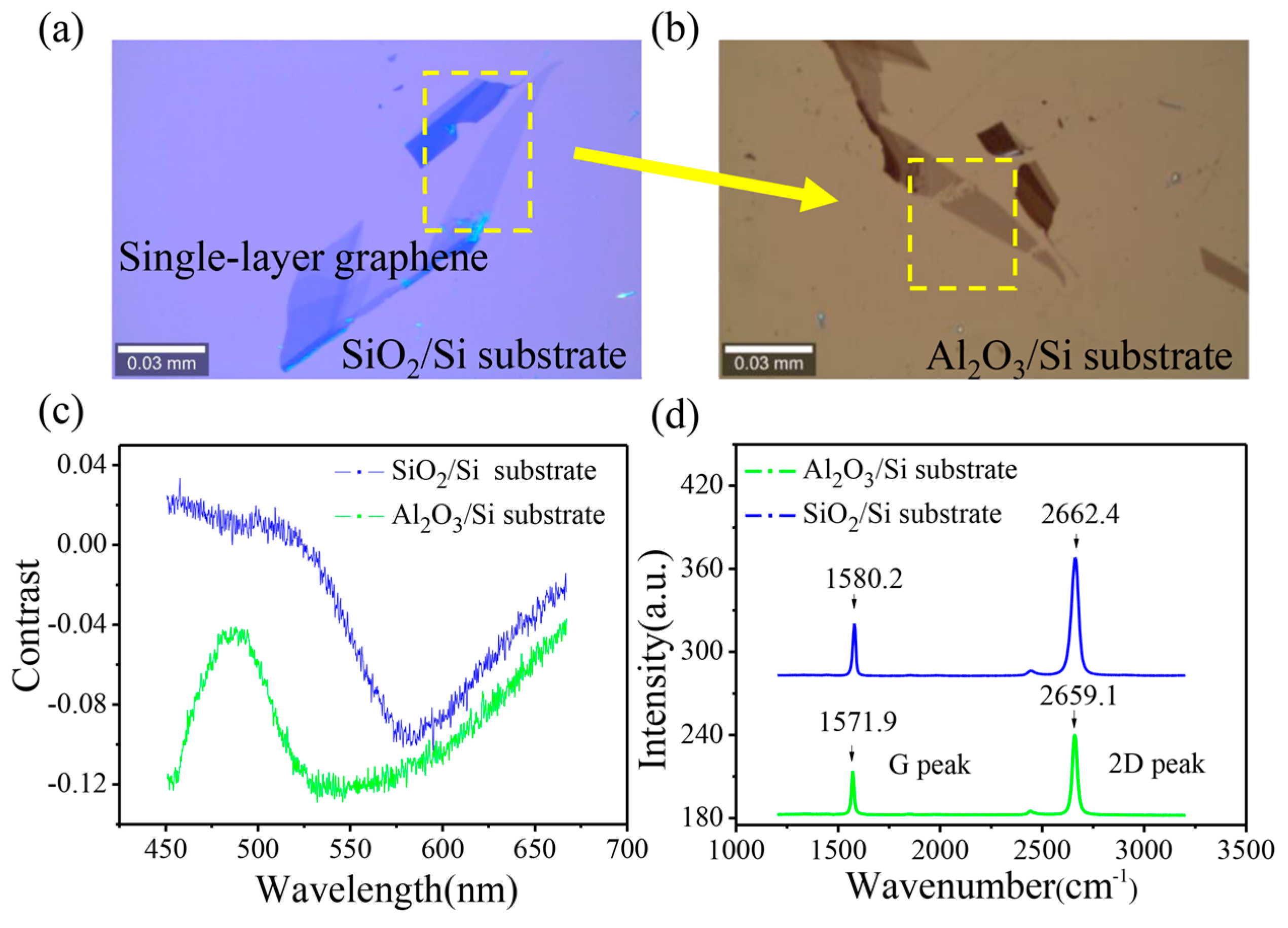
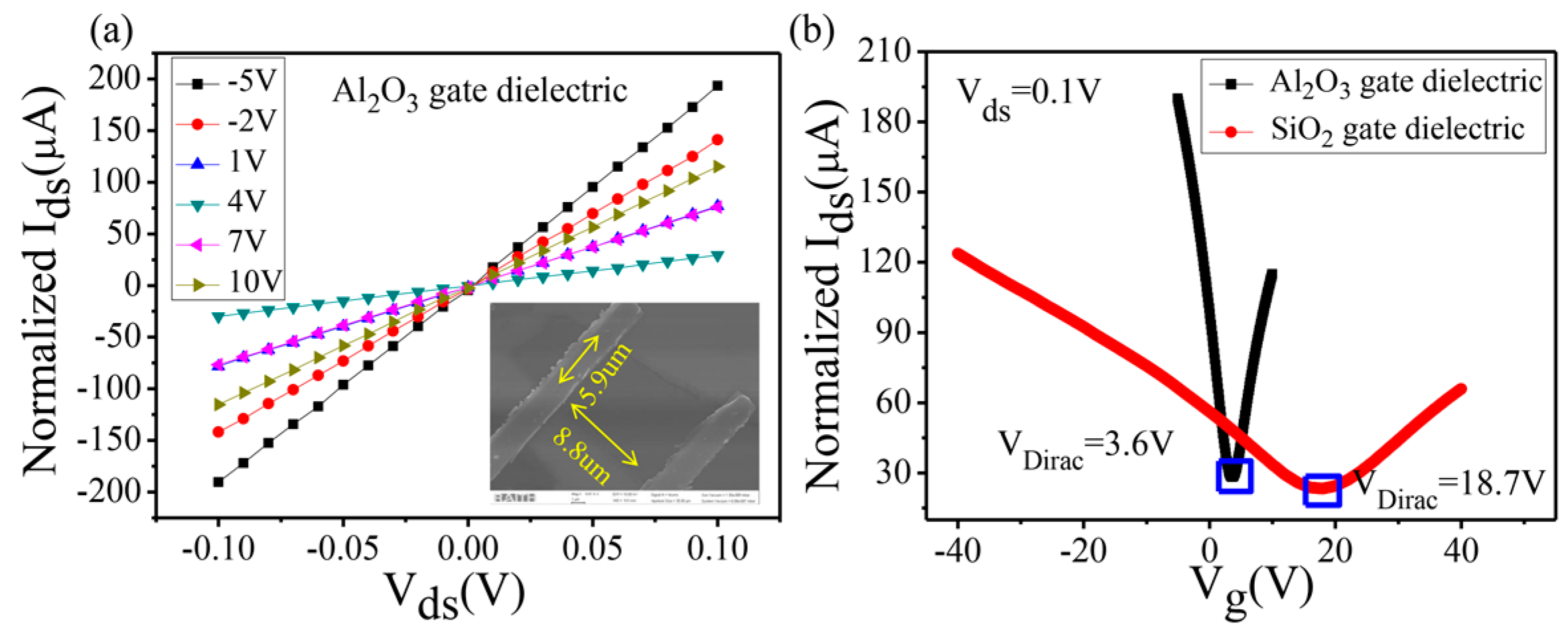
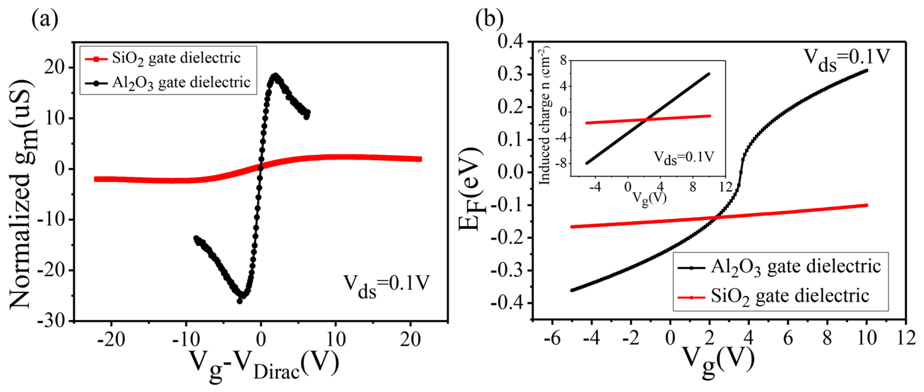
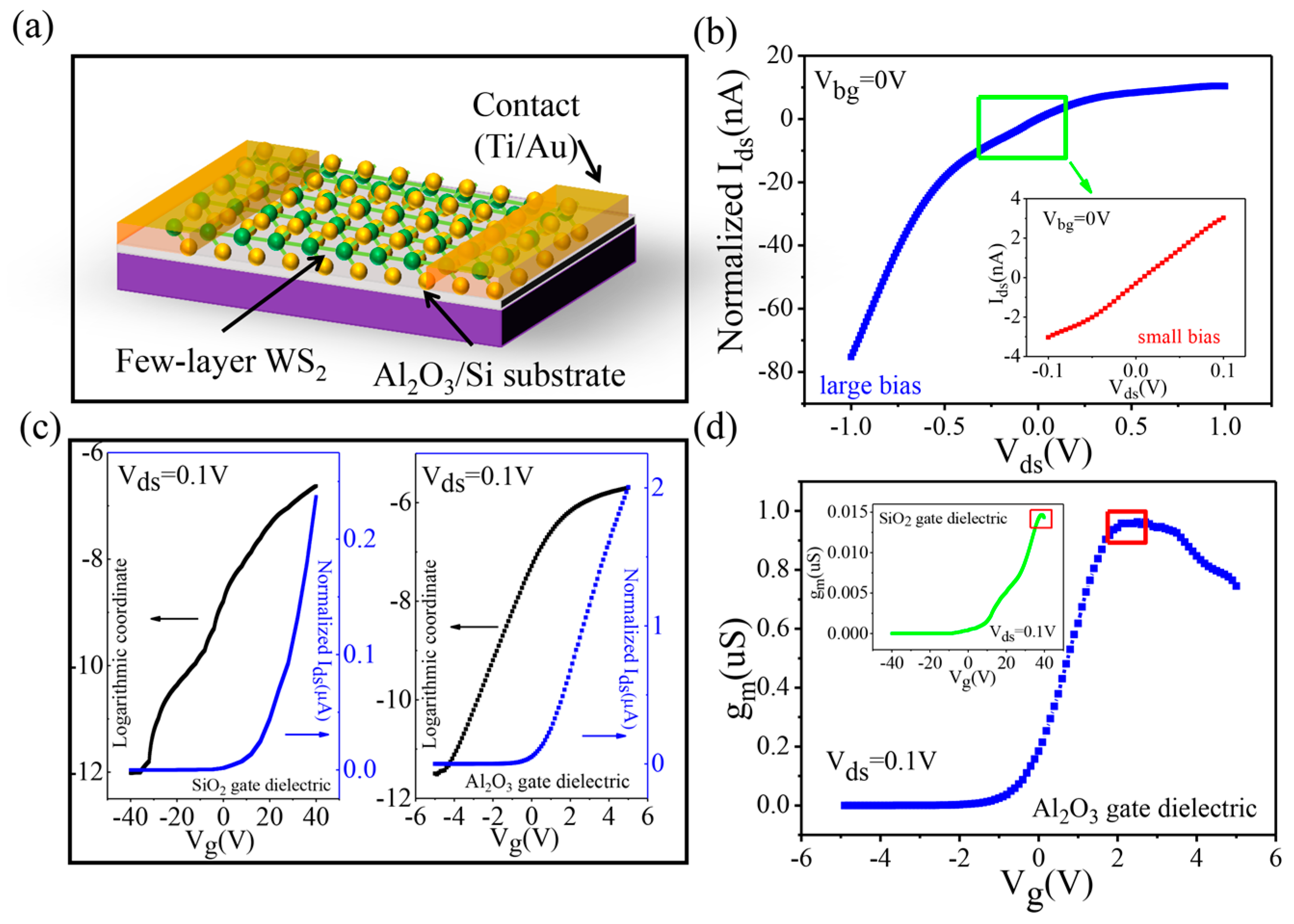
3. Results and Discussion

As shown in Figure 2a, the Al2O3 film is uniform over a large area (50 μ m × 50 μ m). Figure 2b illustrates the height distribution of the local area, which mainly varies from 4 to 6 nm. The parameters of surface roughness are given in Table S1. Based on the measurements, the Si surface is extremely smooth after HF treatment. In addition, the average surface roughness of the ALD-grown Al2O3 film is 1.26 nm.
To understand the dielectric properties of the Al2O3 film, I-V characteristics were firstly measured based on metal-insulator-semiconductor (MIS) devices with Al2O3 and SiO2 insulating layers on silicon wafers (shown in Figure 2c). When bias voltage increased to 10 V, the tunneling current of Al2O3 was only one tenth of that of SiO2. This indicates that the Al2O3 dielectric layer can withstand a higher gate voltage, resulting in greater modulation of the Fermi level of 2D materials. In general, the I-V characteristic of the dielectric layer can be described via Fowler–Nordheim (F–N) tunneling behavior [21,23]:
J = A E o x 2 exp ( B / E o x )
where J is current density, Eox is the electric field, and A and B are constants considering carrier effective mass and barrier height, respectively. Apparently, based on Figure 2d, when the electric field is large, it is in good agreement with the theoretical model [24]. However, in the case of small electric fields, due to the influence of electrical noise in the environment, the experimental curve exhibits fluctuation [19].
Optical contrast is the difference in visual properties that enables us to distinguish an object from other objects and the background. Figure 3a,b shows the optical image of graphene on SiO2/Si and Al2O3/Si substrates, respectively. To quantify the contrast of graphene on different substrates, the color images are converted to gray-scale images. By calculation [25], the absolute value of contrast intensity of graphene on the Al2O3/Si substrate (−0.12) is significantly higher than that on the SiO2/Si substrate (−0.05). Furthermore, from the contrast spectrum shown in Figure 3c, the absolute value of the contrast on the Al2O3/Si substrate in the 450~700 nm wavelength range is always higher than that on the SiO2/Si substrate. The best contrast of graphene on the Al2O3/Si substrate could be obtained with 450 nm and 550 nm illuminations. As depicted in Figure 3d, the G peak and the 2D peak of graphene on the Al2O3/Si substrate experience a red-shift (8.3 cm−1 for G peak and 3.3 cm−1 for 2D peak). The Raman shift could be simplified with the harmonic oscillator model [26]: Δ k = β / m , where Δ k is the Raman shift, β is the mechanical constant, and m is the effective mass. Because of the presence of spotted islands on the Al2O3/Si substrate, a tensile stress is formed onto graphene, which leads to a decrease in β and subsequently the red-shift of the Raman vibration peak of graphene on the Al2O3/Si substrate [26].
Next, the electrical properties of graphene FETs on the Al2O3/Si substrate were studied in nitrogen. As depicted in Figure 4a, the drain-source current (Ids) increases linearly in pace with the bias voltage, indicating good ohmic contact between the graphene and the electrode. The aspect ratio (L/W) of the channel is approximately 1.5, as shown in the SEM image. For better comparison among different samples, normalized Ids (=Ids × L / W ) was applied, which considered the influence of the aspect ratio. Figure 4b shows the transfer characteristics of our devices (Vg means back-gate voltage). It is obvious that the curve slope of the device on the Al2O3/Si substrate is significantly higher than that on the SiO2/Si substrate, indicating a greater gate regulation ability of the 70 nm Al2O3 dielectric layer. In addition, for graphene on the Al2O3/Si substrate, when the gate voltage increases from −5 to 3.6 V, the current decreases from 190 to 28.3 A, so the unit on/off ratio is evaluated to be 0.78 V−1. However, the unit on/off ratio for graphene on the SiO2/Si substrate reaches only 0.09 V−1. Accordingly, the magnification capability was easily estimated to increase by 8.7 times. The minimum conductance on the Al2O3/Si substrate is slightly higher than that on the SiO2/Si substrate, which may be due to induced impurities in the transfer process, leading to more carriers in grapheme [8]. For further discussion, some significant parameters of FETs are listed in Table 1.
The normalized transconductance gm can be extracted from the following [27]:
g m = d I d s d V g L W
The black curve in Figure 5a illustrates the transconductance variation of graphene on the Al2O3/Si substrate. It can be seen that the maximum negative transconductance and maximum positive transconductance are −26.1 μS (Vg = −3.1 V) and 19.4 μS (Vg = 2.9 V), respectively. Compared with the maximum gm of graphene on the SiO2/Si substrate (2.6 μS), it can be concluded that the regulation ability of the Al2O3 dielectric layer is about 10 times that of SiO2, which is in accordance with previous estimations. Accordingly, the value of effective dielectric constant for Al2O3 is 9.2, which is consistent with the theoretical dielectric constant (8~10) of the Al2O3 film grown by ALD [28]. The changes of the Fermi level of graphene can be fitted with the theoretical model [29]:
E F = h v F π n / 2 π q = h v F π ε 0 ε ( V g V D ) / q d / 2 π q
where EF is the Fermi level, n is the induced charge amount, h is the Planck constant, v F is the Fermi speed, q is the elementary charge, and VD is the Dirac point. The amount of charges induced by the applied gate voltages on different substrates is shown in the inset of Figure 5b. Obviously, as the thickness decreases and the dielectric constant increases, the shift of the Fermi level of graphene on the Al2O3/Si substrate is far greater than that on the SiO2/Si substrate. In order to evaluate the mobility of the devices, a device model was used [27]. The extracted carrier mobility of graphene FETs on the Al2O3/Si substrate is 6500 cm2 V−1·s−1, which is similar to 6780 cm2 V−1·s−1 of the FETs on the SiO2/Si substrate. The replacement of the substrate does not lead to the degradation of the transport performance of the devices. Furthermore, transfer characteristic of few-layer graphene FETs on an Al2O3/Si substrate was depicted in Figure S4, showing that Al2O3 gating substrate is also suitable for few-layer graphene.
We also systematically studied the electrical properties of few-layer WS2 on the Al2O3/Si substrate (Figure 6a). The number of layers was determined by Raman and Photoluminescence spectra (see Figure S5). A single layer was not used because the surface states of single-layer TMDs are easily affected by the external environment in the process of device fabrication, thus losing the intrinsic property [30]. As Figure 6b shows, the current varies nonlinearly against the change in bias voltage from −1 to 1 V. This is due to the formation of the Schottky barrier between WS2 and metal contact, which was widely reported in previous studies [30,31,32]. However, from the inset of Figure 6b, it can be seen that the linearity is maintained fairly well under the condition of small bias voltage. Hence, the bias voltage is maintained at 0.1 V in the following test.
Figure 6c illustrates the transfer characteristics of few-layer WS2 on different substrates, and both of them distinctly exhibit n-type behavior conduction [31]. When the gate voltage changes from −10 to 10 V, devices on Al2O3/Si substrates turn from the off state (2.8 pA) to the on state (2.5 μA). Therefore, the unit on/off ratio is as highly as 105 V−1, which is far greater than that on the SiO2/Si substrate (1.5 × 10³ V−1). As depicted in Figure 6d, the maximum transconductance (red rectangle) of few-layer WS2 can reach about 0.92 μS (Vg = 2.3 V), and the corresponding carrier mobility is calculated to be 239 cm2·V−1·s−1. However, as the gate voltage continues to increase, the transconductance starts to decline, indicating that the carrier mobility has reached the maximum value. Compared with the maximum transconductance of few-layer WS2 on the Si/SiO2 substrate (1.5 × 10⁻² μS), the gate control ability was significantly improved (61.3 times). Furthermore, the Al2O3 substrate is a better alternative for other 2D materials (such as WS2).

4. Conclusions

In summary, Al2O3/Si substrates are superior for the visualization of graphene and fabrication of graphene transistors. Compared with SiO2/Si substrates, Al2O3/Si substrates can enhance the optical contrast of graphene by up to 2.4 times. Furthermore, using the Al2O3 film as the gate dielectric, the transconductance of graphene FETs exhibited an approximately 10-fold increase. Significantly, this substrate is also more suitable for other 2D materials, such as WS2, and can remarkably enhance the transconductance by 61.3 times.

Supplementary Materials

The following are available online at https://www.mdpi.com/2079-4991/7/10/286/s1, Figure S1: Steps of deterministic transfer method. Figure S2: Reflection spectra of graphene on different substrates. Figure S3: Raman scanning image of graphene on different substrates. Figure S4: Transfer characteristic and Raman spectrum of few-layer graphene on an Al2O3/Si substrate. Figure S5: Photoluminescence and Raman spectra of few-layer WS2 on Al2O3/Si substrate. Table S1: Average roughness (Sa), root mean square (Sq) and coefficient of kurtosis (Ska) of three different substrates (Si, SiO2, Al2O3).

Acknowledgments

The authors acknowledge financial support from the National Natural Science Foundation of China (Nos. 11574395, 61675234), the Open Foundation of State Key Laboratory of High Performance Computing (No. 201301-02), the Advanced Research Foundation of the National University of Defense Technology (No. zk16-03-40), and the research project of National University of Defense Technology (No. JC15-02-01).

Author Contributions

Hang Yang and Gang Peng conceived and designed the experiments; Hang Yang, Xiaoming Zheng and Yuan Tan performed the experiments; Shiqiao Qin, Guang Wang and Xueao Zhang provided valuable suggestions; Hang Yang wrote the paper. All authors read and approved the final manuscript.

Conflicts of Interest

The authors declare no conflict of interest.

References

  1. Radisavljevic, B.; Radenovic, A.; Brivio, J.; Giacometti, V.; Kis, A. Single-layer MoS2 transistors. Nat. Nanotechnol. 2011, 6, 147–150. [Google Scholar] [CrossRef] [PubMed]
  2. Liao, L.; Lin, Y.C.; Bao, M.; Cheng, R.; Bai, J.; Liu, Y.; Qu, Y.; Wang, K.L.; Huang, Y.; Duan, X. High speed graphene transistors with a self-aligned nanowire gate. Nature 2010, 467, 305–308. [Google Scholar] [CrossRef] [PubMed]
  3. Seyler, K.L.; Schaibley, J.R.; Gong, P.; Rivera, P.; Jones, A.M.; Wu, S.; Yan, J.; Mandrus, D.G.; Yao, W.; Xu, X. Electrical control of second-harmonic generation in a WSe2 monolayer transistor. Nat. Nanotechnol. 2015, 10, 407–411. [Google Scholar] [CrossRef] [PubMed]
  4. Li, Y.; Zhang, H.; Yan, D.W.; Yin, H.-F.; Cheng, X.L. Secondary plasmon resonance in graphene nanostructures. Front. Phys. 2015, 10, 102–108. [Google Scholar] [CrossRef]
  5. Mueller, T.; Xia, F.; Avouris, P. Graphene photodetectors for high-speed optical communications. Nat. Photonics 2010, 4, 297–301. [Google Scholar] [CrossRef]
  6. Hang, Y.; Li, Q.; Luo, W.; He, Y.; Zhang, X.; Peng, G. Photo-Electrical Properties of Trilayer MoSe2 Nanoflakes. Nano 2016, 11, 1650082. [Google Scholar] [CrossRef]
  7. Kim, K.S.; Zhao, Y.; Jang, H.; Lee, S.Y.; Kim, J.M.; Kim, K.S.; Ahn, J.H.; Kim, P.; Choi, J.Y.; Hong, B.H. Large-scale pattern growth of graphene films for stretchable transparent electrodes. Nature 2009, 457, 706. [Google Scholar] [CrossRef] [PubMed]
  8. Kim, Y.; Kwon, Y.J.; Kang, E.L.; Oh, Y.; Um, M.-K.; Seong, D.G.; Lee, J.U. Flexible Textile-Based Organic Transistors Using Graphene/Ag Nanoparticle Electrode. Nanomaterials 2016, 6, 147. [Google Scholar] [CrossRef] [PubMed]
  9. Jung, I.; Pelton, M.; Piner, R.; Dikin, D.A.; Stankovich, S.; Watcharotone, S.; Hausner, M.; Ruoff, R.S. Simple Approach for High-Contrast Optical Imaging and Characterization of Graphene-Based Sheets. Nano Lett. 2007, 7, 3569–3575. [Google Scholar] [CrossRef]
  10. Skulason, H.S.; Gaskell, P.E.; Szkopek, T. Optical reflection and transmission properties of exfoliated graphite from a graphene monolayer to several hundred graphene layers. Nanotechnology 2010, 21, 295709. [Google Scholar] [CrossRef] [PubMed]
  11. Li, H.; Lu, G.; Yin, Z.; He, Q.; Li, H.; Zhang, Q.; Zhang, H. Optical Identification of Single-and Few-Layer MoS2 Sheets. Small 2012, 8, 682–686. [Google Scholar] [CrossRef] [PubMed]
  12. Chen, W.; Qin, S.; Zhang, X.A.; Zhang, S.; Fang, J.; Wang, G.; Wang, C.; Wang, L.; Chang, S. Current induced doping in graphene-based transistor with asymmetrical contact barriers. Appl. Phys. Lett. 2014, 104, 183. [Google Scholar] [CrossRef]
  13. Chen, W.; Qin, S.; Zhang, X.A.; Zhang, S.; Fang, J.; Wang, G.; Wang, C.; Wang, L.; Chang, S. Current self-amplification effect of graphene-based transistor in high-field transport. Carbon 2014, 77, 1090–1094. [Google Scholar] [CrossRef]
  14. Yin, Z.; Li, H.; Li, H.; Jiang, L.; Shi, Y.; Sun, Y.; Lu, G.; Zhang, Q.; Chen, X.; Zhang, H. Single-Layer MoS2 Phototransistors. ACS Nano 2012, 6, 74–80. [Google Scholar] [CrossRef] [PubMed]
  15. Lyu, H.; Lu, Q.; Huang, Y.; Ma, T.; Zhang, J.; Wu, X.; Yu, Z.; Ren, W.; Cheng, H.; Wu, H. Graphene Distributed Amplifiers: Generating Desirable Gain for Graphene Field-Effect Transistors. Sci. Rep. 2015, 5, 17649. [Google Scholar] [CrossRef] [PubMed]
  16. Guerriero, E.; Polloni, L.; Rizzi, L.G.; Massimiliano, B. Graphene audio voltage amplifier. Small 2012, 8, 357–361. [Google Scholar] [CrossRef] [Green Version]
  17. Lee, H.S.; Min, S.W.; Park, M.K.; Lee, Y.T.; Jeon, P.J.; Kim, J.H.; Ryu, S.; Im, S. MoS2 nanosheets for top-gate nonvolatile memory transistor channel. Small 2012, 8, 3111–3115. [Google Scholar] [CrossRef] [PubMed]
  18. Liao, L.; Bai, J.; Cheng, R.; Lin, Y.; Jiang, S.; Huang, Y.; Duan, X. Top-Gated Graphene Nanoribbon Transistors with Ultra-Thin High-k Dielectrics. Nano Lett. 2010, 10, 1917–1921. [Google Scholar] [CrossRef] [PubMed]
  19. Alaboson, J.M.P.; Wang, Q.H.; Emery, J.D.; Lipson, A.L.; Bedzyk, M.J.; Elam, J.W.; Pellin, M.J.; Hersam, M.C. Seeding atomic layer deposition of high-k dielectrics on epitaxial graphene with organic self-assembled monolayers. ACS Nano 2011, 5, 5223–5232. [Google Scholar] [CrossRef] [PubMed]
  20. Xuan, Y.; Wu, Y.Q.; Shen, T.; Qi, M.; Capano, M.A.; Cooper, J.A.; Ye, P.D. Atomic-layer-deposited nanostructures for graphene-based nanoelectronics. Appl. Phys. Lett. 2008, 92, 013101. [Google Scholar] [CrossRef]
  21. Liao, L.; Bai, J.; Qu, Y.; Huang, Y.; Duan, X. Single-layer graphene on Al2O3/Si substrate: Better contrast and higher performance of graphene transistors. Nanotechnology 2010, 21, 015705. [Google Scholar] [CrossRef] [PubMed]
  22. Dean, C.R.; Young, A.F.; Meric, I.; Lee, C.; Wang, L.; Sorgenfrei, S.; Watanabe, K.; Taniguchi, T.; Kim, P.; Shepard, K.L.; et al. Boron nitride substrates for high-quality graphene electronics. Nat. Nanotechnol. 2010, 5, 722–726. [Google Scholar] [CrossRef] [PubMed]
  23. Liao, L.; Bai, J.; Qu, Y.; Lin, Y.C.; Li, Y.; Huang, Y.; Duan, X. High-κ oxide nanoribbons as gate dielectrics for high mobility top-gated graphene transistors. Proc. Natl. Acad. Sci. USA 2010, 107, 6711–6715. [Google Scholar] [CrossRef] [PubMed]
  24. Fallahazad, B.; Lee, K.; Lian, G.; Kim, S.; Corbet, C.M.; Ferrer, D.A.; Colombo, L.; Tutuc, E. Scaling of Al2O3 dielectric for graphene field-effect transistors. Appl. Phys. Lett. 2012, 100, 093112. [Google Scholar] [CrossRef]
  25. Ni, Z.H.; Wang, H.M.; Kasim, J.; Fan, H.M.; Yu, T.; Wu, Y.H.; Feng, Y.P.; Shen, Z.X. Graphene thickness determination using reflection and contrast spectroscopy. Nano Lett. 2007, 7, 2758–2763. [Google Scholar] [CrossRef] [PubMed]
  26. Zheng, X.; Chen, W.; Wang, G.; Yu, Y.; Qin, S.; Fang, J.; Wang, F.; Zhang, X. The Raman redshift of graphene impacted by gold nanoparticles. AIP Adv. 2015, 5, 1530–1534. [Google Scholar] [CrossRef]
  27. Giubileo, F.; di Bartolomeo, A.; Martucciello, N.; Romeo, F.; Iemmo, L.; Romano, P.; Passacantando, M. Contact Resistance and Channel Conductance of Graphene Field-Effect Transistors under Low-Energy Electron Irradiation. Nanomaterials 2016, 6, 206. [Google Scholar] [CrossRef] [PubMed]
  28. Groner, M.D.; Elam, J.W.; Fabreguette, F.H.; George, S.M. Electrical characterization of thin Al2O3 films grown by atomic layer deposition on silicon and various metal substrates. Thin Solid Films 2002, 413, 186–197. [Google Scholar] [CrossRef]
  29. Rao, C.N.; Sood, A.K.; Subrahmanyam, K.S.; Govindaraj, A. Graphene: The new two-dimensional nanomaterial. Angew. Chem. Int. Ed. 2009, 48, 7752–7777. [Google Scholar] [CrossRef] [PubMed]
  30. Huo, N.; Yang, S.; Wei, Z.; Li, S.; Xia, J.; Li, J. Photoresponsive and Gas Sensing Field-Effect Transistors based on Multilayer WS2 Nanoflakes. Sci. Rep. 2014, 4, 5209. [Google Scholar] [CrossRef] [PubMed]
  31. Cui, Y.; Xin, R.; Yu, Z.; Pan, Y.; Ong, Z.; Wei, X.; Wang, J.; Nan, H.; Ni, Z.; Wu, Y. High-Performance Monolayer WS2 Field-Effect Transistors on High-κ Dielectrics. Adv. Mater. 2015, 27, 5230–5234. [Google Scholar] [CrossRef] [PubMed]
  32. Ying, C.; Sun, H.; Peng, W. 2D Transition Metal Dichalcogenides and Graphene-Based Ternary Composites for Photocatalytic Hydrogen Evolution and Pollutants Degradation. Nanomaterials 2017, 7, 62. [Google Scholar]
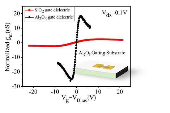
Figure 1. The process of fabricating graphene (or WS2) field effect transistors (FETs) on Al2O3/Si substrates. HF: hydrofluoric acid.
Nanomaterials 07 00286 g001
Figure 2. Characterization of 70 nm Al2O3 film prepared by atomic layer deposition (ALD). (a) Atomic force microscopy (AFM) image and corresponding (b) height distribution of film surface (areas in blue dashed box). (c) Tunneling currents of Al2O3 and SiO2 films. (d) Flow–Nordheim (F–N) fitting curve of the metal-insulator-semiconductor (MIS) device.
Nanomaterials 07 00286 g002
Figure 3. (a,b) Optical image of graphene on the SiO2/Si and Al2O3/Si substrates. (c) The contrast and (d) Raman spectra of graphene on SiO2/Si and Al2O3/Si substrates. Raw data and processing methods are shown in Figures S2 and S3.
Nanomaterials 07 00286 g003
Figure 4. (a) Output characteristics of graphene FETs on the Al2O3/Si substrate at different gate voltages (−5~10 V). The inset shows an SEM image of the device. (b) Transfer characteristics of graphene FETs on different substrates.
Nanomaterials 07 00286 g004
Figure 5. (a) gmVg curves of graphene FETs on different substrates. (b) EFVg curves of graphene FETs on different substrates. The inset shows the variation tendency of the induced charge against gate voltage.
Nanomaterials 07 00286 g005
Figure 6. (a) Three-dimensional schematic view of the few-layer WS2 FETs. (b) Output characteristics of few-layer WS2 on Al2O3/Si substrates in large bias and (inset) small bias voltage. (c) Transfer characteristics of few-layer WS2 FETs on different substrates. (d) gmVg curves of few-layer WS2 FETs on different substrates.
Nanomaterials 07 00286 g006
Table 1. Significant parameters of graphene FETs on different substrates.
ParametersMinimum ConductivityDirac PointMaximum TrascondutanceMobility
Substrate
Al2O3283 μS3.6 V−26.1 μS6500 cm2 V−1·s−1
SiO2237 μS18.7 V2.6 μS6780 cm2 V−1·s−1

