N-Doped Graphene with Low Intrinsic Defect Densities via a Solid Source Doping Technique


1
State Key Laboratory of Electronic Thin Films and Integrate Devices, University of Electronic Science and Technology of China, Chengdu 610054, China
2
Department of Electronic Engineering, Chang Gung University, Taoyuan 33302, Taiwan
3
Institute of Electro-Optical Engineering, Chang Gung University, Taoyuan 33302, Taiwan
4
Biosensor Group, Biomedical Engineering Research Center, Chang Gung University, Taoyuan 33302, Taiwan
5
Department of General Surgery, Chang Gung Memorial Hospital, Linkou 33305, Taiwan
6
Department of Nephrology, Chang Gung Memorial Hospital, Linkou 33305, Taiwan
7
Department of Materials Engineering, Ming Chi University of Technology, New Taipei City 24301, Taiwan
*
Author to whom correspondence should be addressed.
†
These authors contributed equally to this work.
Nanomaterials 2017, 7(10), 302; https://doi.org/10.3390/nano7100302
Submission received: 18 August 2017
/
Revised: 19 September 2017
/
Accepted: 25 September 2017
/
Published: 30 September 2017
Abstract
:N-doped graphene with low intrinsic defect densities was obtained by combining a solid source doping technique and chemical vapor deposition (CVD). The solid source for N-doping was embedded into the copper substrate by NH3 plasma immersion. During the treatment, NH3 plasma radicals not only flattened the Cu substrate such that the root-mean-square roughness value gradually decreased from 51.9 nm to 15.5 nm but also enhanced the nitrogen content in the Cu substrate. The smooth surface of copper enables good control of graphene growth and the decoupling of height fluctuations and ripple effects, which compensate for the Coulomb scattering by nitrogen incorporation. On the other hand, the nitrogen atoms on the pre-treated Cu surface enable nitrogen incorporation with low defect densities, causing less damage to the graphene structure during the process. Most incorporated nitrogen atoms are found in the pyrrolic configuration, with the nitrogen fraction ranging from 1.64% to 3.05%, while the samples exhibit low defect densities, as revealed by Raman spectroscopy. In the top-gated graphene transistor measurement, N-doped graphene exhibits n-type behavior, and the obtained carrier mobilities are greater than 1100 cm2·V−1·s−1. In this study, an efficient and minimally damaging n-doping approach was proposed for graphene nanoelectronic applications.

1. Introduction
Graphene is a promising next generation electronic material, and its electronic properties can be modified by the substitutional doping of heteroatoms (e.g., boron [1], nitrogen [2], fluorine [3], and sulfur [4]). Among these atoms, nitrogen, which forms stable covalent bonds due to its similar atomic size and introduces an additional n-type valance electron, is widely used as the heteroatom for adjusting graphene properties. Nitrogen substitution doping in the graphene lattice gives rise to potential applications in fuel cells [5], lithium ion batteries [6], molecular sensors [7], ultracapacitors [8], and nanoelectronics [9] because nitrogen atoms disrupt the intrinsic graphene hybridization and locally induce significant modifications to its charge distribution and chemical reactivity [10]. Furthermore, with nitrogen doping, the work function of graphene shifts to lower states [11], providing broad and adjustable band applications in graphene p-n junctions [12] and mixed-dimensional van der Waals structures [13] (2D-iD, i = 0, 1, 2, 3, e.g., graphene-quantum dots, graphene-carbon nanotubes (CNTs), graphene-2D materials, and graphene-bulk materials). To obtain these promising properties and applications, researchers have continuously endeavored to synthesis N-doped graphene without damaging the graphene crystal structure and deteriorating its carrier mobility.
The synthesis methods for N-doped graphene can be briefly classified into two main categories [14]: (i) post-treatment in which nitrogen is incorporated into graphene or graphene oxide by post-annealing in NH3 gas or by NH3 plasma [7,11,15,16,17] or via Ultraviolet illumination in NH3 [18] and (ii) direct doping during synthesis in which carbon/nitrogen precursors such as CH4/H2/NH3 [19] and pyridine [9] are simultaneously introduced during the graphene growth, specifically in chemical vapor deposition (CVD). Despite the achievements in the successful synthesis of N-doped graphene in which the graphene properties can be tailored and the crystal structure can be preserved, the incorporation processes are always accompanied by high defect densities and graphene carrier mobility degradation. For the transport mechanism, the presence of additional structural defects and the process of nitrogen incorporation activate short-range (intrinsic lattice defects) and long-range scattering (ionized impurities or ripples), respectively [20,21]. Therefore, the transport behavior of N-doped graphene is strongly dependent on its synthesis process, including the nitrogen doping process and the accompanying formation of defects.
To obtain N-doped graphene with low defect densities, Cory et al. determined the ion energy window for nitrogen doping in the graphene lattice with the balance between the substitutional reaction efficiency and the vacancies or defect formation [22]. Moreover, George et al. proposed a high-temperature (between 1150 to 1200 °C) post-annealing method for efficient nitrogen doping with negligible defect densities [23]. During the high-temperature post-annealing in NH3, covalent C–N bonds form at intrinsic defects, vacancies or sites with weak C–C bonds in which the carbon atoms can be easily replaced by nitrogen atoms. However, considering the mismatch of the thermal expansion coefficients between graphene and the underlying substrate and the electrical disturbance induced by the closer contact between graphene and the underlying substrate after high-temperature post-annealing, extensive research must be devoted to its transport performance after high-temperature post-annealing [24]. For the method of direct doping during growth, two main challenges still remain for the realization of N-doped graphene with low defect densities. First, the mixed flow of carbon and nitrogen precursors in the gas phase triggers a competition between nitrogen incorporation and the NHx group-based etching effect that induces increased defect densities [23]. The second is the growth temperature-dependent trade-off between the intrinsic defect densities and the nitrogen doping efficiency; while the nitrogen doping efficiency was found to be the largest at low temperatures (600 to 880 °C), the use of these temperatures increases the risk of the formation of intrinsic defects and localized bi-layer or few layer fractions. On the other hand, highly crystallized graphene can be synthesized at elevated temperatures (>950 °C), but the presence of NHx groups was limited during the growth process [19,25]. The formation of low defect densities in N-doped graphene substantially weakens its induced short-range scattering, but a method for the synthesis of N-doped graphene without transport degradation is still lacking.
To overcome the bottleneck in the direct synthesis of N-doped graphene in the conventional chemical vapor deposition (CVD) process and to obtain high transport properties for N-doped graphene, a solid state doping technique was introduced in this study. The solid state doping technique is broadly used for efficient and uniform doping with low amounts of structural defects in low dimensional materials, such as nanowires and conducting polymers [26,27,28]; however, this technique has rarely been studied experimentally in monolayer graphene decoration [29]. In the current study, Cu foil was chosen as the substrate for monolayer graphene growth owing to its low solubility of carbon. Cu foils were pre-treated by NH3 plasma at room temperature, and atomic force microscopy (AFM) was performed to examine the surface morphology variation. This process embeds nitrogen atoms into the Cu substrate, which are subsequently used as the solid-state doping source. Then, N-doped graphene was grown by CVD on the nitrogen-doped copper substrate. X-ray photoelectron spectroscopy (XPS) and Raman spectroscopy were used to analyze the bonding and lattice properties of N-doped graphene. Top-gated graphene field-effect transistors (GFETs) were fabricated using N-doped graphene as the channel, and 1100 cm2·V−1·s−1 carrier mobilities were achieved without carrier mobility degradation, which is comparable to the corresponding pristine graphene.
2. Results and Discussion
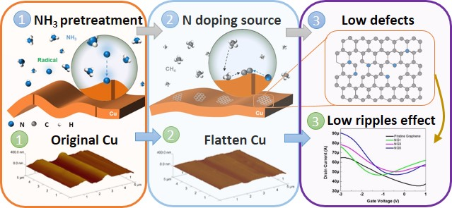
Figure 1 shows the illustration of the NH3 pretreatment and N-doped graphene synthesis. As illustrated in Figure 1a, during NH3 plasma treatment, nitrogen radicals are embedded into the Cu surface, and N–Cu bonds are formed after the surface oxidation and after the organic residues were reduced by hydrogen radicals in the NH3 plasma [30,31]. Meanwhile, the Cu surface was flattened during the plasma treatment [32]. The critical point of N–Cu bond formation commonly started after 20 s to 30 s of the NH3 plasma treatment [30,31], and a high N/Cu ratio of over 10% could be achieved at the Cu surface [33]. Then, the Cu foils with and without NH3 plasma pretreatment were loaded into a low-pressure chemical vapor deposition (LPCVD) chamber for graphene growth separately, as shown in Figure 1b (details are given in the Methods section).
The distinct apparent morphologies of these Cu foil samples with different NH3 plasma pretreatment times, acquired in a 5 μm × 5 μm area prior to graphene CVD growth, are shown in Figure 2a–d. The original Cu foil without the NH3 plasma pretreatment exhibits a periodically corrugated structure with a maximum height of 202.4 nm and a surface roughness with a root mean square (RMS) value of 51.9 nm. Samples with an NH3 plasma pretreatment of 1, 3, and 5 min were labelled as NG1, NG3, and NG5, respectively. The Cu surface morphology becomes less rough as the NH3 plasma pretreatment time increases. For the Cu with a 1, 3, and 5 min plasma treatment, the height of the Cu surface corrugation structure and surface roughness decrease to 46.2 nm and 15.5 nm, respectively. The surface-flattening effect of the plasma treatment is comparable to the effects of other Cu pretreatment processes, such as electrochemical polishing or pre-annealing [34]. After the large domain synthesis is complete, graphene and N-doped graphene are transferred onto the SiO2 substrate for further measurement and analysis (CVD growth and transfer processes are performed following our previous work, and the details are in the Methods section).
To investigate the bonding configurations of N atoms in the graphene lattice, XPS was performed on pristine graphene and N-doped graphene samples after transfer onto the SiO2 substrates. The deconvoluted C1s spectra of pristine graphene and NG1 are shown in Figure 3a,b, respectively (Figure S1a,b show the C1s spectra of NG3 and NG5, respectively). The main peak located at 284.6 eV indicates that most C atoms were arranged in the conjugated honeycomb lattice configurations for each sample. In addition to the main peak, peaks at 285.8, 286.1, 287.6, 288.9 eV corresponding to C–N, C–O, C=O, and O–C=O, respectively, were observed; these peaks are attributed to nitrogen doping and organic residues or oxygen absorption. The N1s spectrum is typically used to elucidate the nitrogen dopant configurations in the graphene lattice [35]. As shown in Figure 3c, the N1s spectrum for NG1 can be deconvoluted into two components, pyrrolic N at 400.0 eV and graphitic N at 401.5 eV (detailed N1s spectra for NG3 and NG5 are shown in Figure S1c,d), which is consistent with other CVD approaches (a brief summary of nitrogen doping configurations is given in Table 1). The inset of Figure 3c shows the N1s spectrum of pristine graphene in the N1s spectrum for comparison, demonstrating that the nitrogen doping in the graphene lattice originated from the NH3 plasma pretreatment on the Cu surface. Note that the hydrogen annealing process may remove some surface nitrogen atoms. However, based on these results, the amount of surface nitrogen is sufficient for the graphene dopants. As shown in Figure 3d, the nitrogen concentrations of N-doped graphene were 3.05%, 1.95%, and 1.64%, for samples NG1, NG3, and NG5, respectively, which was partially contributed by graphitic N with values of 0.59%, 0.55%, and 0.16%, respectively. The discrepancy between the decreased doping efficiency trend and the increased plasma treatment duration could be ascribed to the substrate-flattening effect by NH3 plasma. According to the recent report on atomic-level scanning tunneling microscopy (STM) analysis, nitrogen atoms are preferentially located at the graphene grain boundaries, while there is no indication of nitrogen in the atomically flat graphene regions [36]. Thus, the opportunity for nitrogen doping in rough Cu surface regions is higher than the opportunity in flat Cu surface regions.
N-doped graphene samples were also analyzed using their Raman spectra in the 1200–3000 cm−1 range as shown in Figure 4. There are four typical graphene vibrational modes in the Raman spectrum: (a) a D peak at 1350 cm−1 (defect mode), (b) a G peak at 1586 cm−1 (vertical vibration mode), (c) a D’ peak at 1620 cm−1 (disorder mode), and (d) a 2D peak at 2707 cm−1 (two-phonon vibration mode). The locations of the G peak and the 2D peak of pristine graphene and N-doped graphene are shown in Figure 4a,b. Compared to pristine graphene, N-doped graphene samples (NG1, NG3, and NG5) show a downshift of the G peak from 1586 to 1582, 1582, and 1584 cm−1, respectively, and a downshift of the 2D peak from 2707 to 2701, 2701, and 2701 cm−1, respectively, indicating n-type doping from pristine graphene to NG1, NG3, and NG5 [37]. The I2D/IG ratios for both pristine graphene and N-doped graphene were greater than 2, as shown in Figure 4a, indicating the high quality and crystallinity of the samples. Derived from the data shown in Figure 4a, the ID/IG ratios of pristine graphene and N-doped graphene range from 0.168 to 0.171, 0.173, and 0.191. Based on the ID/IG ratio, the defect density for each sample can be calculated using the average defect distances based on the Tuinstra-Koenig (TK) relation of [2] (2.4 × 10⁻¹⁰)λ4(ID/IG)−1 as 71.4 nm (pristine graphene), 70.1 nm (NG1), 69.3 nm (NG3), and 62,8 nm (NG5). The slightly increasing trend of defect mode intensity is consistent with our XPS survey because more structural defects are induced by pyrrolic N than graphitic N. Moreover, the D’ peak (intra-valley double resonance, which is activated by defects) is weak compared to the G peak, indicating that a relatively low disorder accompanies the nitrogen doping [38]. The incorporation of pyrrolic N is always accompanied by the appearance of structural defects. Pyrrolic N bonds to two sp2-hybridized carbon neighbors with adjacent carbon vacancies. In addition, nitrogen incorporation may influence and even interact with the defect formation process during the kinetic growth of graphene because the nitrogen atoms are predominantly distributed at grain boundary regions where defects and vacancies are also easily formed to release the interfacial stress originating from the lattice mismatch between Cu and graphene [36]. The interaction between the released interfacial stress and nitrogen incorporation is reduced by the current pretreatment approach because the pre-existing nitrogen atoms on the Cu surface do not mix with the CH4 gas in the processes of gas phase deposition, molecular decomposition, and long-range Cu surface kinetic diffusion.
For comparison, the same plasma treatment process was directly applied to the graphene samples after the transfer onto SiO2 substrates. The graphene samples without and with NH3 plasma in 1, 3, and 5 min treatments were also examined by Raman spectroscopy, and the Raman spectra are shown in Figure S2. Under 1 and 3 min NH3 plasma treatments, strong lattice structural damage was found in which splitting was observed for the D and G peaks, and the 2D peak showed an obvious decrease. For the graphene samples under a 5 min NH3 plasma treatment, the typical vibration modes of graphene (D, G, and 2D) almost disappeared. During the NH3 plasma treatment directly on graphene, high additional plasma energy after nitrogen displacement remained in the graphene lattice and transferred into in-plane collisions [22]. Thus, the lattice structure was severely damaged as the treatment time increased.
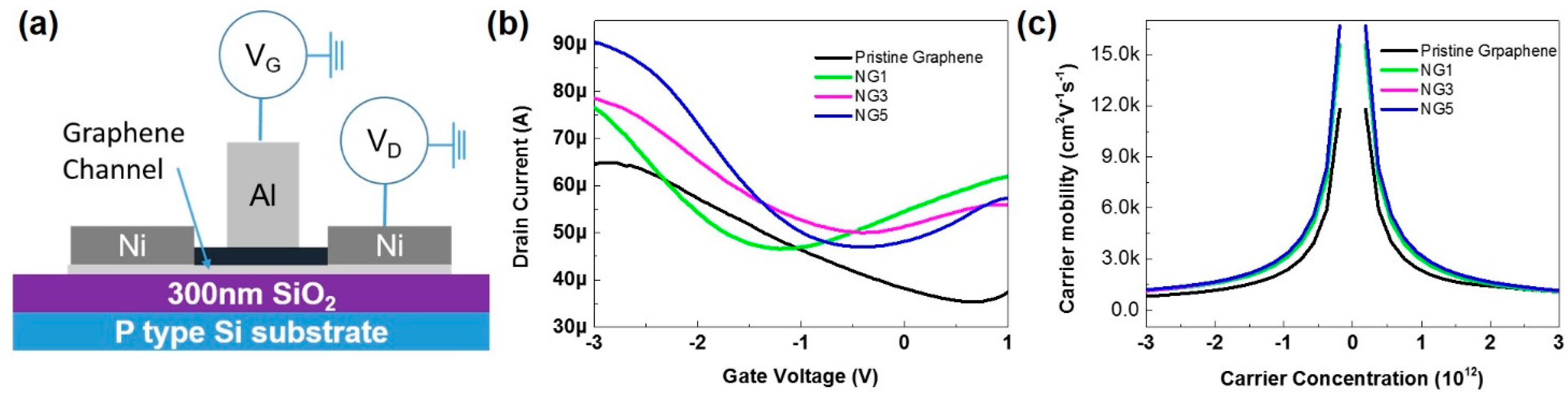
Finally, to measure the electrical properties, a top-gated GFET was fabricated, as shown in Figure 5a (the details of the fabrication process are given in the Methods section). The source and drain metal contact created by Ni can form an ohmic contact with graphene, as clearly shown in the IdVd curves in Figure S3b. The contact resistivity between Ni and CVD graphene was determined using the transfer length method in the range of 0.7 to 7 kΩ·µm [39,40,41]. Based on this range, the contact resistance could be 1.2% to 12% of the total resistance. Aluminum oxide was chosen as the gate dielectric owing to its high isolation property and low charge transfer effects with graphene (Figure S3a). Figure 5b shows the drain current versus gate voltage curves of each graphene transistor under a gate sweep from −2.5 V to 1.5 V and with the drain voltage fixed at 0.1 V. The Dirac point of pristine graphene was located at 0.7 V, and for the N-doped graphene samples, Dirac points were n-type shifted to −1.2 V (NG1), −0.4 V (NG3), and −0.2 V (NG5). The trend of the Dirac point shift is consistent with the N-doping efficiency, as revealed by the XPS survey. Both pyrrolic and graphitic N were attributed to n-type doping behaviors [20]. In graphitic and pyrrolic N-doping configurations, three valence electrons of the nitrogen atoms are necessary to form bonds with their carbon neighbors, and the remaining two valence electrons provide additional charges to the conduction band, giving rise to n-type doping. Based on the IdVg measurement results and the capacitance of graphene transistors shown in Figure 5b and Figure S3c, the carrier mobility of each sample can be derived in terms of the Drude formula () as a function of the carrier density ( = Cg(Vg − VDirac)/e), where is the resistance and Cg is the gate dielectric capacitance [42]. As shown in Figure 5c, the hole mobilities of pristine graphene, NG1, NG3, and NG5 were 809, 1131, 1134, and 1201 cm2·v−1·s−1 (at 3 × 10¹²/cm2), respectively. The electron mobilities of pristine graphene, NG1, NG3, and NG5 were 1060, 1061, 1121, and 1151 cm2·v−1·s−1 (at 3 × 10¹²/cm2), respectively. The opposite ambipolar mobility behaviors of pristine graphene and N-doped graphene can be clarified using Novikov’s calculation showing that attractive scattering is dominant relative to the repulsive scattering for Dirac fermions in graphene [43]. Therefore, for N-doped graphene, the dominant scattering centers are positive ions, while for the p-type pristine graphene, the asymmetry is different from the N-doped graphene samples. Moreover, a higher carrier mobility and conductivity is shown by N-doped graphene than by pristine graphene. These N-doped graphene samples were synthesized on a pre-treated, flattened Cu surface, while pristine graphene was grown on the original Cu surface. The flattened Cu foil weakens the ripple effect of graphene because graphene grows along the apparent contour of the Cu surface [21,34]. For comparison, the FET of the graphene under 1, 3, and 5 min NH3 plasma treatments was also fabricated, and no Id–Vg curves were obtained because the graphene was severely damaged during the direct high-energy plasma treatment.
A brief comparison of the N-doped graphene with different CVD synthesis approaches is presented in Table 1, including the parameters of the synthesis conditions, nitrogen concentrations and configurations, ID/IG ratios, Dirac points, and carrier mobilities. Starting with exfoliated graphene, followed by ion implantation and high-temperature NH3 annealing, N-doped graphene exhibits a high mobility, reaching 6000 cm2·V−1·s−1. However, this post-annealing doping method for pristine graphene results in a relatively low doping concentration, possibly due to the low probability of graphene interface hybridization between nitrogen atoms and the continuous atomic lattice structure [2,23]. For CVD graphene, which could be manipulated in large-area electronic applications, the N-doping concentration can be adjusted from 2.4% to 16% by precursors or by synthesis conditions. Nitrogen dopant incorporated into the graphene lattice via CVD is mostly found in pyrrolic and pyridinic configurations, which are always accompanied by an increase in defect densities and an increased ID/IG ratio to values ranging from 0.3 to 2 (few-layered N-doped graphene shows a lower ID/IG due to a high vertical phonon vibration nature). Both nitrogen incorporation (ionic impurities, long-range scattering) [44] and its accompanied increase in defect densities (bonding disorder and vacancies, short-range scattering) [45] degrade graphene carrier conductivity and mobility [20]. Recently, George Sarau et al. realized N-doped graphene with a low defect density via the post-annealing approach in which the nitrogen atoms are mostly arranged in pyridinic configurations [23]. Compared with pyrrolic nitrogen, pyridinic nitrogen shows a higher similarity to the original graphene lattice; however, a higher formation energy and synthesis temperature are required for the process [19]. In this study, low defect density N-doped graphene with a pyrrolic dominated nitrogen configuration achieved by combining CVD and the solid source doping technique is proposed. First, low defect density reduces short-range scattering in graphene. Second, the flat Cu surface reduces height fluctuations for 2D graphene [21,34], compensating for the long-range scattering caused by ionic nitrogen incorporation. The current carrier mobility of N-doped graphene is comparable to that found in previous studies: 200–450 cm2·v−1·s−1 (CVD with a mixed gas precursor) [35], 100–400 cm2·v−1·s−1 (plasma enhanced CVD-grown) [17], 365 cm2·v−1·s−1 (pyridine annealing on Cu) [46], and 1050 cm2·v−1·s−1 (substrate doping) [37]. Note that the current study is based on top-gated transistor structures rather than the traditional back-gated graphene transistors using thick SiO2 as the gate dielectric, which is more compatible with the integrated circuit (IC) architectures and operates in the low gate voltage mode, but the trade-off is the series resistance in the access region.
3. Conclusions
In summary, a CVD synthesis process for low defect density N-doped graphene based on the NH3 plasma pretreatment of the Cu foil catalyst was proposed. Approximately 80% of the nitrogen dopant atoms in the graphene lattice are present in the pyrrolic configuration, and the nitrogen concentration was negatively correlated with Cu surface roughness. For synthesis on the pre-treated Cu catalyst, N-doping does not induce a high density of defects or disorder in the graphene lattice, as revealed by the Raman spectra. The electrical transport measurement shows that N-doping effectively modulates the electrical properties of graphene to n-type behavior with high conductivity and carrier mobility. This study provides a low defect density approach for N-doped graphene synthesis and significantly advances the modulation and improvement of the performance of graphene in nanoelectronic applications.
4. Methods
4.1. NH3 Plasma Pretreatment and AFM Scanning
Cu foil (99.8% purity, 25 μm, Alfa Aesar, Ward Hill, MA, USA) was loaded into the plasma-enhanced CVD (PECVD) system, and the chamber was evacuated to 2 mTorr at room temperature. NH3 flowed into the chamber at 20 sccm while the pressure was maintained at 0.5 Torr, and radio frequency power of 100 W was applied to generate the NH3 plasma. The degree of plasma treatment of each sample was adjusted by controlling the exposure time (from 1 min to 5 min) after the plasma was ignited. The Cu surface morphology was scanned using an Innova AFM (Bruker Company, Billerica, MA, USA) equipped with an Olympus AC160TS probe (tip radius of 7 nm, Kuboyama-cho, Hachioji-shi, Tokyo, Japan). The AFM tip was operated in tapping mode and set to map a 5 × 5 μm2 area across the samples.
4.2. Graphene Growth and Transfer Process
Copper foils with and without NH3 plasma pretreatment were loaded into a low-pressure tube furnace separately [50]. The growth temperature was set to 1000 °C under a H2 flow rate of 50 standard cubic centimeters per minute (sccm, cm3/min) to remove the native Cu oxide. Then, 20 sccm CH4 was introduced to grow graphene on the Cu foils for 20 min. After the graphene synthesis was complete, the furnace was cooled to room temperature at a rate of ~5 °C/s. A layer of polymethyl methacrylate (PMMA) was spin-coated onto the graphene on the Cu surface. The films were then treated with a Cu etchant and rinsed with deionized (DI) water before they were transferred to the 300 nm SiO2/Si substrates. The PMMA support layer was removed from each film using acetone, and the remaining graphene films were rinsed with isopropyl alcohol.
4.3. Raman Spectral Analysis and X-ray Photoelectron Spectroscopy
Raman spectra were collected using a RAMaker confocal Raman microscope system (PROTRUSTECH, east district, Tainan, Taiwan, laser excitation photon energy of ~2.62 eV; laser spot-size of ~0.5 μm). The Raman peak of Si at 520 cm−1 was used as the calibration signal for each sample. For Raman probing, each sample was exposed for 3 s, which was repeated 3 times to obtain an average value and to eliminate unintentional cosmic ray effects. The chemical configurations were determined using an X-ray photoelectron spectrometer (VG Scientific, Microlab 350, East Grinstead, UK) with an Auger electron beam gun (LEG 300-F electron column). The energies were calibrated relative to the C1s peak to eliminate the charge distribution of the sample during analysis.
4.4. Top-Gated Graphene Field-Effect Transistors Fabrication and Measurement
After transferring the graphene onto the 300 nm SiO2/Si substrate, 50 nm of Ni was deposited as the source and drain (100 μm × 100 μm). The graphene channel (20 µm in width and 50 µm in length) was patterned using lithography methods followed by an O2 plasma etching step; finally, 1500 nm of Al was deposited followed by a 1.5-nm Al deposition as a buffer layer. Both of these Al layers were exposed to air for more than 8 h to form a thin AlOx dielectric layer between the graphene channel and the Al gate [51]. Graphene transistors were measured using a B1500-Agilent semiconductor analyzer (Santa Clara, CA, USA).
Supplementary Materials
The following are available online at https://www.mdpi.com/2079-4991/7/10/302/s1, Figure S1: XPS spectra for N-doped graphene. (a,b) C1s core level for NG3 and NG5; (c,d) N1s core level for NG3 and NG5. Figure S2: Raman spectrum of graphene without and with a 1 min, 3 min, and 5 min NH3 plasma treatment. Figure S3: (a) The Ig/Vg curve of pristine graphene and N-doped graphene; (b) the Id/Vd curve of pristine graphene and N-doped graphene; (c) gate capacitance of pristine graphene and N-doped graphene, the inset illustration shows the structure of the capacitance measurement.
Acknowledgments
This research was supported by the Ministry of Science and Technology, Taiwan (106-2221-E-182-059-MY3, 106-2632-E-182-001, and 106-2911-I-182-504), Chang Gung Memorial Hospital (CMRPD2F0022 and CMRPD2G0101).
Author Contributions
Bo Liu carried out literature search, experiments, figures drawing, data collection, data analysis, organization and writing. Chia-Ming Yang performed data analysis, organization and writing. Zhiwei Liu performed data analysis and manuscript revision. Chao-Sung Lai initiated the idea, designed the study, and performed data analysis, organization and manuscript revision.
Conflicts of Interest
The authors declare no conflict of interest.
References
- Agnoli, S.; Favaro, M. Doping graphene with boron: A review of synthesis. J. Mater. Chem. A Mater. Energy Sustain. 2016, 4, 5002–5025. [Google Scholar] [CrossRef]
- Guo, B.; Liu, Q.; Chen, E.; Zhu, H.; Fang, L.; Gong, J.R. Controllable N-doping of graphene. Nano Lett. 2010, 10, 4975–4980. [Google Scholar] [CrossRef] [PubMed]
- Ho, K.I.; Liao, J.H.; Huang, C.H.; Hsu, C.L.; Zhang, W.; Lu, A.Y.; Li, L.J.; Lai, C.S.; Su, C.Y. One-step formation of a single atomic-layer transistor by the selective fluorination of a graphene film. Small 2014, 10, 989–997. [Google Scholar] [CrossRef] [PubMed]
- Liang, C.; Wang, Y. Synthesis of sulfur-doped p-type graphene by annealing with hydrogen sulfide. Carbon 2014, 82, 506–512. [Google Scholar] [CrossRef]
- Choi, K.; Lee, S.; Shim, Y.; Oh, J.; Kim, S.; Park, S. Electrocatalytic performances of N-doped graphene with anchored iridium species in oxygen reduction reaction. 2D Mater. 2015, 2, 34019. [Google Scholar] [CrossRef]
- Chem, J.M.; Ma, C.; Cao, D. Nitrogen-doped graphene nanosheets as anode materials for lithium ion batteries: A first-principles study. J. Mater. Chem. 2012, 22, 8911–8915. [Google Scholar]
- Lv, R.; Li, Q.; Botello-Méndez, A.R.; Hayashi, T.; Wang, B.; Berkdemir, A.; Hao, Q.; Elías, A.L.; Cruz-Silva, R.; Gutiérrez, H.R.; et al. Nitrogen-doped graphene: Beyond single substitution and enhanced molecular sensing. Sci. Rep. 2012, 2, 586. [Google Scholar] [CrossRef] [PubMed]
- Jeong, H.M.; Lee, J.W.; Shin, W.H.; Choi, Y.J.; Shin, H.J.; Kang, J.K.; Choi, J.W. Nitrogen-Doped Graphene for High-Performance Ultracapacitors and the Importance of Nitrogen-Doped Sites at Basal Planes. Nano Lett. 2011, 11, 2472–2477. [Google Scholar] [CrossRef] [PubMed]
- Jin, Z.; Yao, J.; Kittrell, C.; Tour, J.M. Large-scale growth and characterizations of nitrogen-doped monolayer graphene sheets. ACS Nano 2011, 5, 4112–4117. [Google Scholar] [CrossRef] [PubMed]
- Meyer, J.C.; Kurasch, S.; Park, H.J.; Skakalova, V.; Künzel, D.; Gross, A.; Chuvilin, A.; Algara-siller, G.; Roth, S.; Iwasaki, T.; et al. Experimental anaysis of charge redistribution due to chemical bonding by high resolution transmission electron microscopy. Nat. Mater. 2011, 10, 209–215. [Google Scholar] [CrossRef] [PubMed]
- Boutchich, M.; Arezki, H.; Alamarguy, D.; Ho, K.-I.; Sediri, H.; Güneş, F.; Alvarez, J.; Kleider, J.P.; Lai, C.S.; Ouerghi, A. Atmospheric pressure route to epitaxial nitrogen-doped trilayer graphene on 4H-SiC (0001) substrate. Appl. Phys. Lett. 2014, 105, 233111. [Google Scholar] [CrossRef]
- Lin, L.; Liao, L.; Yin, J.; Peng, H.; Liu, Z. Building graphene p–n junctions for next-generation photodetection. Nano Today 2015, 10, 701–716. [Google Scholar] [CrossRef]
- Jariwala, D.; Marks, T.J.; Hersam, M.C. Mixed-dimensional van der Waals heterostructures. Nat. Mater. 2017, 16, 170–181. [Google Scholar] [CrossRef] [PubMed]
- Wang, H.; Maiyalagan, T.; Wang, X. Review on Recent Progress in Nitrogen-Doped Graphene: Synthesis, Characterization, and Its Potential Applications. ACS Catal. 2012, 2, 781–794. [Google Scholar] [CrossRef]
- Li, X.; Wang, H.; Robinson, J.T.; Sanchez, H.; Diankov, G. Simultaneous Nitrogen Doping and Reduction of Graphene Oxide. J. Am. Chem. Soc. 2009, 131, 15939–15944. [Google Scholar] [CrossRef] [PubMed]
- Lin, Y.; Ksari, Y.; Aubel, D.; Hajjar-garreau, S.; Spiegel, Y.; Roux, L.; Simon, L.; Themlin, J. Efficient and low-damage nitrogen doping of graphene via plasmabased methods. Carbon 2016, 100, 337–344. [Google Scholar] [CrossRef]
- Wei, D.; Peng, L.; Li, M.; Mao, H.; Niu, T.; Han, C.; Chen, W.; Wee, A.T.S. Low Temperature Critical Growth of High Quality Nitrogen Doped Graphene on Dielectrics by Plasma-Enhanced Chemical Vapor Deposition. ACS Nano 2015, 9, 164–171. [Google Scholar] [CrossRef] [PubMed]
- Imamura, G.; Saiki, K. Effect of UV light-induced nitrogen doping on the field effect transistor characteristics of graphene. RSC Adv. 2015, 5, 70522–70526. [Google Scholar] [CrossRef]
- Sui, Y.; Zhu, B.; Zhang, H.; Shu, H.; Chen, Z.; Zhang, Y.; Zhang, Y.; Wang, B.; Tang, C.; Xie, X.; et al. Temperature-dependent nitrogen configuration of N-doped graphene by chemical vapor deposition. Carbon 2014, 81, 814–820. [Google Scholar] [CrossRef]
- Lu, Y.-F.; Lo, S.-T.; Lin, J.-C.; Zhang, W.; Lu, J.-Y.; Liu, F.-H.; Tseng, C.-M.; Lee, Y.-H.; Liang, C.-T.; Li, L.-J. Nitrogen-Doped Graphene Sheets Grown by Chemical Vapor Deposition: Synthesis and Influence of Nitrogen Impurities on Carrier Transport. ACS Nano 2013, 7, 6522–6532. [Google Scholar] [CrossRef] [PubMed]
- Fasolino, A.; Katsnelson, M.I. Intrinsic ripples in graphene. Nat. Mater. 2007, 6, 6–9. [Google Scholar] [CrossRef] [PubMed] [Green Version]
- Cress, C.D.; Schmucker, S.W.; Friedman, A.L.; Dev, P.; Culbertson, J.C.; Lyding, J.W.; Robinson, J.T. Nitrogen doped graphene and twisted bilayer graphene via hyperthermal ion implantation with depth control. ACS Nano 2016, 10, 3714–3722. [Google Scholar] [CrossRef] [PubMed]
- Christiansen, S.; Fau, E.; Staudtstrasse, B. Efficient Nitrogen Doping of Single-Layer Graphene Accompanied by Negligible Defect Generation for Integration into Hybrid Semiconductor Heterostructures. ACS Appl. Mater. 2017, 9, 10003–10011. [Google Scholar]
- Liu, B.; Chiu, I.; Lai, C. Improvements on thermal stability of graphene and top gate graphene transistors by Ar annealing. Vaccum 2017, 137, 8–13. [Google Scholar] [CrossRef]
- Zhang, S.; Tsuzuki, S.; Ueno, K.; Dokko, K.; Watanabe, M. Upper Limit of Nitrogen Content in Carbon Materials. Angew. Chem. Int. Ed. 2015, 54, 1302–1306. [Google Scholar] [CrossRef] [PubMed]
- Moselund, K.E.; Ghoneim, H.; Schmid, H.; Bj, M.T. Solid-state diffusion as an efficient doping method for silicon nanowires and nanowire field effect transistors. Nanotechnology 2010, 21, 435202. [Google Scholar] [CrossRef] [PubMed]
- Resasco, J.; Dasgupta, N.P.; Rosell, J.R.; Guo, J.; Yang, P. Uniform Doping of Metal Oxide Nanowires Using Solid State. J. Am. Chem. Soc. 2014, 136, 10521–10526. [Google Scholar] [CrossRef] [PubMed]
- Kang, K.; Watanabe, S.; Broch, K.; Sepe, A.; Brown, A.; Nasrallah, I.; Nikolka, M.; Fei, Z.; Heeney, M.; Matsumoto, D.; et al. Sirringhaus, 2D coherent charge transport in highly ordered conducting polymers doped by solid state diffusion. Nat. Mater. 2016, 15, 896. [Google Scholar] [CrossRef] [PubMed]
- Zhang, C.; Fu, L.; Liu, N.; Liu, M.; Wang, Y.; Liu, Z. Synthesis of nitrogen-doped graphene using embedded carbon and nitrogen sources. Adv. Mater. 2011, 23, 1020–1024. [Google Scholar] [CrossRef] [PubMed]
- Noguchi, J.; Ohashi, N.; Jimbo, T.; Yamaguchi, H.; Takeda, K.; Hinode, K. Effect of NH3-Plasma Treatment and CMP Modification on TDDB Improvement in Cu. IEEE Trans. Electron Devices 2001, 48, 1340–1345. [Google Scholar] [CrossRef]
- Chang, Y.; Leu, J.; Lin, B.; Wang, Y.; Cheng, Y. Comparison of H2 and NH3 Treatments for Copper Interconnects. Adv. Mater. Sci. Eng. 2013, 2013, 825195. [Google Scholar] [CrossRef]
- Junhwan, O.; Lee, S.; Kim, J.; Lee, C. Effects of Plasma Cleaning of the Cu Seed Layer Surface on Cu Electroplating. J. Korean Phys. Soc. 2001, 39, 472–477. [Google Scholar]
- Vairagar, A.V.; Gan, Z.; Shao, W.; Mhaisalkar, S.G.; Li, H.; Tu, K.N.; Chen, Z.; Zschech, E.; Engelmann, H.J.; Zhang, S. Improvement of Electromigration Lifetime of Submicrometer Dual-Damascene Cu Interconnects Through Surface Engineering. J. Electrochem. Soc. 2006, 153, 840–845. [Google Scholar] [CrossRef]
- Lee, D.; Kwon, G.D.; Kim, J.H.; Moyen, E.; Lee, Y.H.; Baik, S.; Pribat, D. Significant enhancement of the electrical transport properties of graphene films by controlling the surface roughness of Cu foils before and during chemical vapor deposition. Nanoscale 2014, 6, 12943–12951. [Google Scholar] [CrossRef] [PubMed]
- Wei, D.; Liu, Y.; Wang, Y.; Zhang, H.; Huang, L.; Yu, G. Synthesis of n-doped graphene by chemical vapor deposition and its electrical properties. Nano Lett. 2009, 9, 1752–1758. [Google Scholar] [CrossRef] [PubMed]
- Wang, C.; Schouteden, K.; Wu, Q.; Li, Z. Atomic resolution of nitrogen-doped graphene on Cu foils. Nanotechnology 2016, 27, 1–9. [Google Scholar] [CrossRef] [PubMed]
- Xu, W.; Lim, T.S.; Seo, H.K.; Min, S.Y.; Cho, H.; Park, M.H.; Kim, Y.H.; Lee, T.W. N-doped graphene field-effect transistors with enhanced electron mobility and air-stability. Small 2014, 10, 1999–2005. [Google Scholar] [CrossRef] [PubMed]
- Ferrari, A.C.; Basko, D.M. Raman spectroscopy as a versatile tool for studying the properties of graphene. Nat. Nanotechnol. 2013, 8, 235–246. [Google Scholar] [CrossRef] [PubMed]
- Leong, W.S.; Gong, H.; Thong, J.T.L. Low-Contact-Resistance Graphene Devices with Nickel-Etch. ACS Nano 2014, 8, 994–1001. [Google Scholar] [CrossRef] [PubMed]
- Giubileo, F.; Di, A. Progress in Surface Science The role of contact resistance in graphene field-effect devices. Prog. Surf. Sci. 2017, 92, 143–175. [Google Scholar] [CrossRef]
- Bartolomeo, A.D.; Santandrea, S.; Giubileo, F.; Romeo, F.; Petrosino, M.; Citro, R.; Barbara, P.; Lupina, G.; Schroeder, T.; Rubino, A. Effect of back-gate on contact resistance and on channel conductance in graphene-based field-effect transistors. Diam. Relat. Mater. 2013, 38, 19–23. [Google Scholar] [CrossRef]
- Lee, K.H.; Shin, H.; Lee, J.; Lee, I.; Kim, G.; Choi, J.; Kim, S. Large-Scale Synthesis of High-Quality Hexagonal Boron Nitride Nanosheets for Large-Area Graphene Electronics. Nano Lett. 2012, 12, 714–718. [Google Scholar] [CrossRef] [PubMed]
- Novikov, D.S. Numbers of donors and acceptors from transport measurements in graphene. Appl. Phys. Lett. 2009, 91, 666. [Google Scholar] [CrossRef]
- Ho, K.I.; Boutchich, M.; Su, C.Y.; Moreddu, R.; Sebastian, E.S.; Marianathan, R.; Montes, L.; Lai, C.S. A Self-Aligned High-Mobility Graphene Transistor: Decoupling the Channel with Fluorographene to Reduce Scattering. Adv. Mater. 2015, 27, 6519. [Google Scholar] [CrossRef] [PubMed]
- Chen, J.; Cullen, W.G.; Jang, C.; Fuhrer, M.S.; Williams, E.D. Defect Scattering in Graphene. Phys. Rev. Lett. 2009, 102, 236805. [Google Scholar] [CrossRef] [PubMed]
- He, B.; Ren, Z.; Qi, C.; Yan, S.; Wang, Z. Synthesis of nitrogen-doped monolayer graphene with high transparent and n-type electrical properties. J. Mater. Chem. C 2015, 3, 6172–6177. [Google Scholar] [CrossRef]
- Luo, Z.; Lim, S.; Tian, Z.; Shang, J.; Lai, L.; MacDonald, B.; Fu, C.; Shen, Z.; Yu, T.; Lin, J. Pyridinic N doped graphene: Synthesis, electronic structure, and electrocatalytic property. J. Mater. Chem. 2011, 21, 8038–8044. [Google Scholar] [CrossRef]
- Li, J.; Ren, Z.; Zhou, Y.; Wu, X.; Xu, X.; Li, W.; Bai, J.; Wang, L.; Qi, M. Scalable synthesis of pyrrolic N-doped graphene by atmospheric pressure chemical vapor deposition and its terahertz response. Carbon 2013, 62, 330–336. [Google Scholar] [CrossRef]
- Qu, L.; Liu, Y.; Baek, J.B.; Dai, L. Nitrogen-doped graphene as efficient metal-free electrocatalyst for oxygen reduction in fuel cells. ACS Nano 2010, 4, 1321–1326. [Google Scholar] [CrossRef] [PubMed]
- Ho, K.-I.; Huang, C.-H.; Liao, J.-H.; Zhang, W.; Li, L.-J.; Lai, C.-S.; Su, C.-Y. Fluorinated Graphene as High Performance Dielectric Materials and the Applications for Graphene Nanoelectronics. Sci. Rep. 2014, 4, 5893. [Google Scholar] [CrossRef] [PubMed]
- Lu, C.-C.; Lin, Y.-C.; Yeh, C.-H.; Huang, J.-C.; Chiu, P.-W. High Mobility Flexible Graphene Field-Effect Transistors with Self-Healing Gate Dielectrics. ACS Nano 2012, 6, 4469–4474. [Google Scholar] [CrossRef] [PubMed]
Figure 1.
Schematic of (a) NH3 plasma pretreatment of the Cu surface and (b) N-doped graphene synthesis on the pre-treated Cu surface using low-pressure chemical vapor deposition (LPCVD).
Figure 1.
Schematic of (a) NH3 plasma pretreatment of the Cu surface and (b) N-doped graphene synthesis on the pre-treated Cu surface using low-pressure chemical vapor deposition (LPCVD).
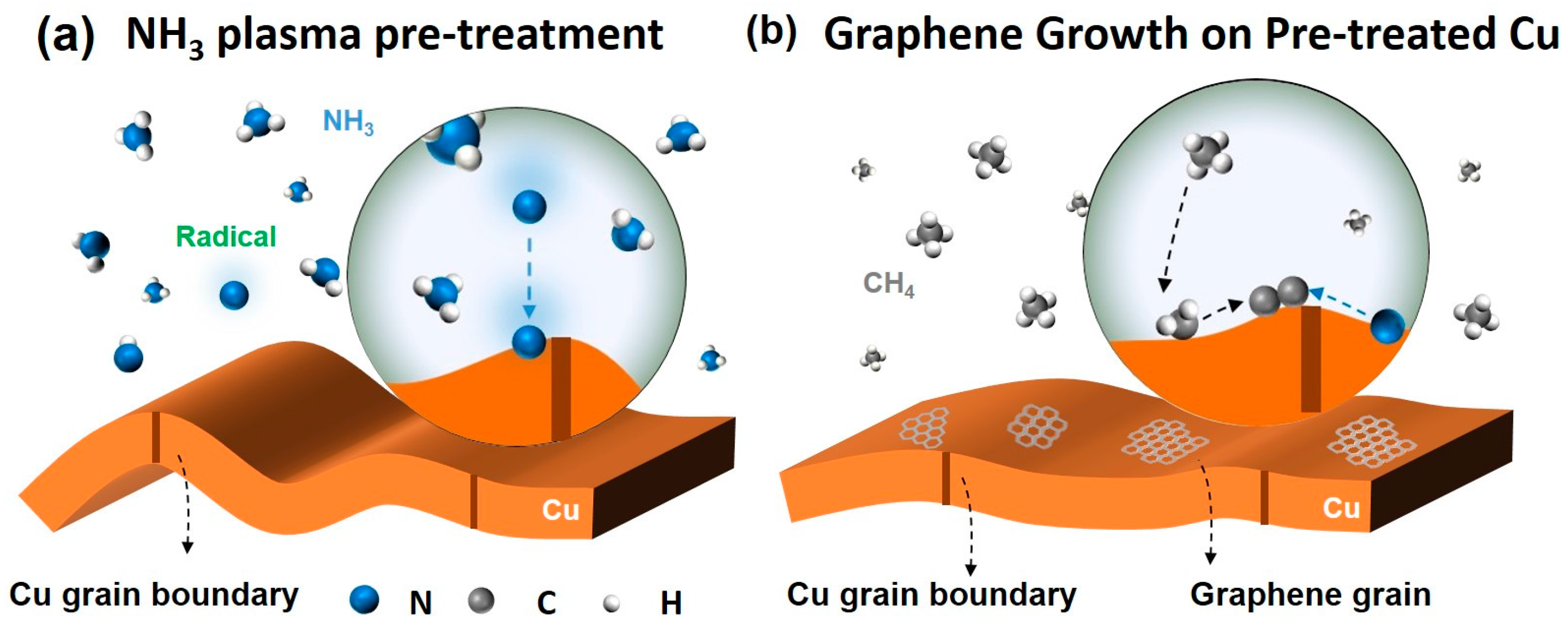
Figure 2.
Atomic force microscopy (AFM) images of the Cu surface without and with NH3 plasma treatment for different durations: (a) original Cu, (b) 1 min, (c) 3 min, and (d) 5 min. RMS is the abbreviation of roughness mean square.
Figure 2.
Atomic force microscopy (AFM) images of the Cu surface without and with NH3 plasma treatment for different durations: (a) original Cu, (b) 1 min, (c) 3 min, and (d) 5 min. RMS is the abbreviation of roughness mean square.
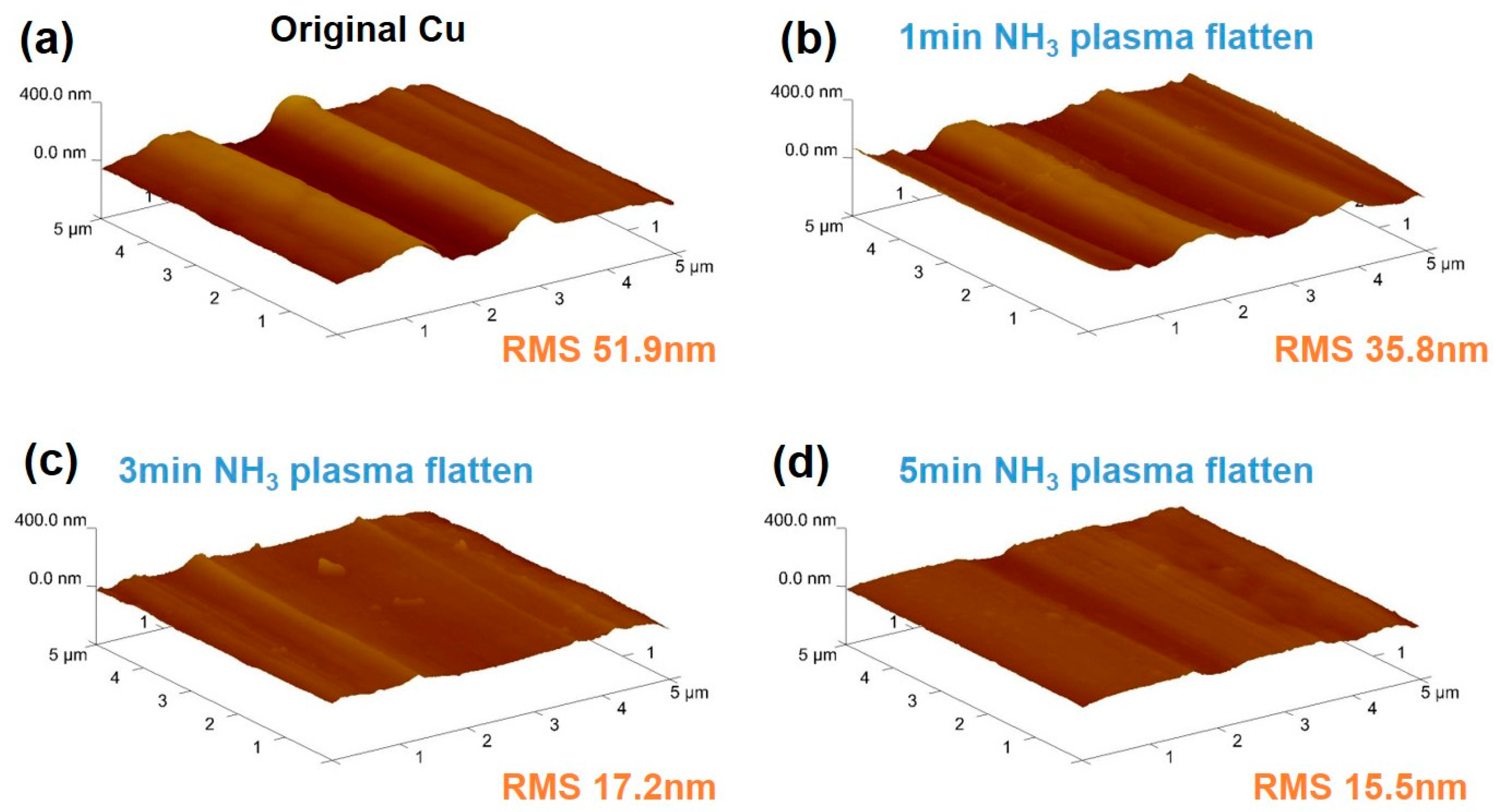
Figure 3.
Analysis of X-ray photoelectron spectroscopy (XPS) spectra for pristine graphene and N-doped graphene. (a,b) C1s spectrum for pristine graphene and NG1; (c) N1s core level for NG1 (inset is the N1s spectrum for pristine graphene); (d) N content ratio and graphitic configuration ratio for NG1, NG3, and NG5.
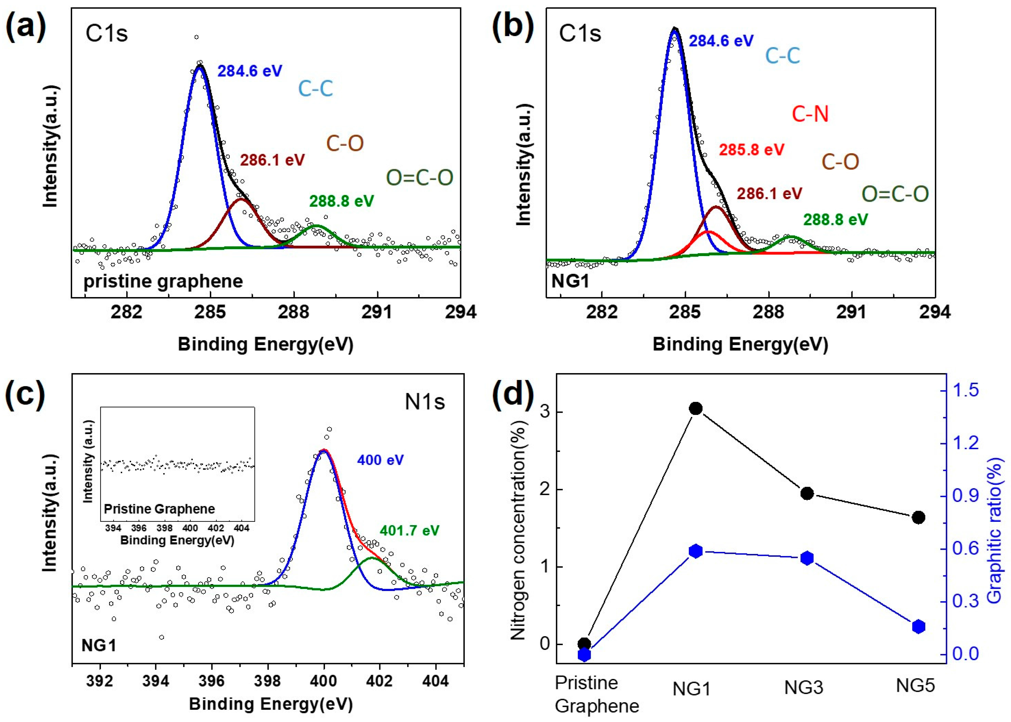
Figure 4.
Raman spectra for pristine graphene and N-doped graphene. (a) Raman spectrum and (b) G and 2D band positions (derived from the Raman spectra).
Figure 4.
Raman spectra for pristine graphene and N-doped graphene. (a) Raman spectrum and (b) G and 2D band positions (derived from the Raman spectra).
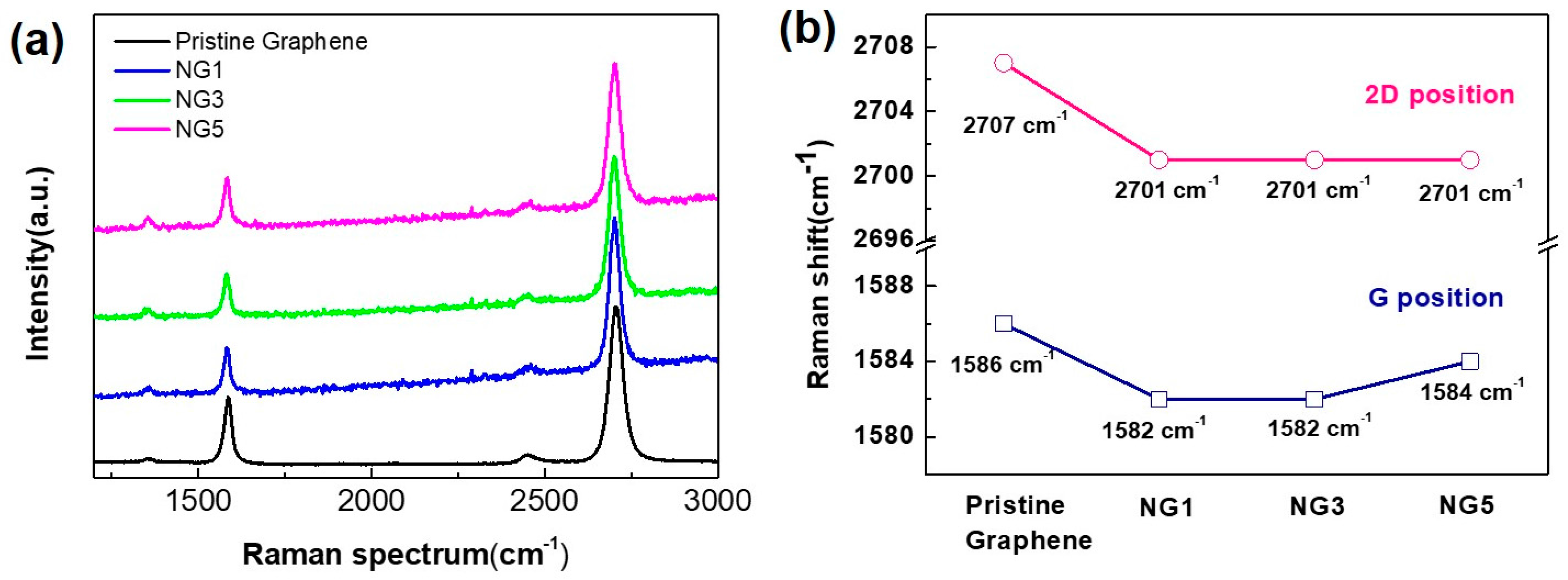
Figure 5.
Transport characteristics for pristine graphene and N-doped graphene. (a) Schematic structure of top-gated graphene field-effect transistors (GFETs) (b) Id–Vg curves for pristine, NG1, NG3, and NG5 FETs, with the drain voltage maintained at 0.1 V and a gate voltage sweep from −2.5 to 1 V; and (c) Mobility as a function of carrier density for pristine graphene, NG1, NG3, and NG5 FETs.


Table 1.
Comparison of N-doping and the electrical performance for N-doped graphene obtained using different growth approaches.
Table 1.
Comparison of N-doping and the electrical performance for N-doped graphene obtained using different growth approaches.
| N-Doped Graphene Synthesis Method | Synthesis Temperature | Nitrogen Content (*) | Nitrogen Configurations (#) | ID/IG | Dirac Point Shift | Carrier mobility N-Doped Graphene/Pristine Graphene (cm2·V−1·s−1) | Ref. |
|---|---|---|---|---|---|---|---|
| CVD monolayer graphene growth on NH3 plasma pre-treated Cu foil | 1000 °C | 3% | Pyrrolic, Graphitic | 0.17 | 0.7 to −1.2 V (top gate) | ~1100/~1000 (electron branch) ~1100/800 (hole branch) | This work |
| CVD monolayer graphene growth on Cu using C2H2, H2 and NH3 as precursors | 900 °C | 16% | Pyridinic | >2 | N/A | N/A | [47] |
| CVD monolayer graphene growth on Cu using CH4 and NH3 as precursors | 1000 °C | 6.4% | Pyrrolic | ~0.7 | N/A | N/A | [48] |
| CVD monolayer graphene growth on Cu (CH4 + NH3) | 800 °C | 8.9% | Graphitic | ~0.30 | N/A | 450/1200 | [35] |
| CVD few-layered (2–8 layers) graphene growth on Ni (CH4 + NH3 + Ar) | 1000 °C | 4% | Pyrrolic, Pyridinic | 0.06–0.25 | N/A | N/A | [49] |
| CVD few-layered graphene growth on Ni with embedded nitrogen | 1000 °C | 2.9% | Pyrrolic, Pyridinic, Graphitic | 2.1 | more than 60 to −50 V (back gate) | N/A | [29] |
| CVD on Cu using pyridine as the precursor | 1000 °C | 2.4% | Pyridinic, Pyrrolic | 0.3–0.4 | 10 to −10 V (back gate) | 5/2000 | [9] |
| PECVD growth of NG on SiO2/Si using C2H2 and NH3 plasma as precursors | 475 °C | N/A | Pyridinic | ~0.7 | 20 to −20 V (back gate) | 400/NA | [17] |
| Post-annealing of CVD graphene (on Cu foil) in NH3 gas | 850 °C | 0.25% | Pyrrolic, Pyridinic | ~1 | N/A | N/A | [7] |
| Exfoliated graphene with N2 ion implantation and post-annealing in NH3 | 1100 °C | 1.1% | Pyridinic | ~0.6 | ~2 V to ~−7 V (back gate) | 6000/6700 (electron branch) 6000/15000 (hole branch) | [2] |
(*) Only the highest nitrogen content samples were chosen in each study; (#) The nitrogen configurations were sequenced by the nitrogen content ratio for each study. The nitrogen pyridinic, pyrrolic, and graphitic configurations accounted for a binding energy of approximately 398.2, 400.3, and 401.5 eV, respectively. CVD = chemical vapor deposition. PECVD = plasma-enhanced CVD.
© 2017 by the authors. Licensee MDPI, Basel, Switzerland. This article is an open access article distributed under the terms and conditions of the Creative Commons Attribution (CC BY) license (http://creativecommons.org/licenses/by/4.0/).
Share and Cite
MDPI and ACS Style
Liu, B.; Yang, C.-M.; Liu, Z.; Lai, C.-S. N-Doped Graphene with Low Intrinsic Defect Densities via a Solid Source Doping Technique. Nanomaterials 2017, 7, 302. https://doi.org/10.3390/nano7100302
AMA Style
Liu B, Yang C-M, Liu Z, Lai C-S. N-Doped Graphene with Low Intrinsic Defect Densities via a Solid Source Doping Technique. Nanomaterials. 2017; 7(10):302. https://doi.org/10.3390/nano7100302
Chicago/Turabian StyleLiu, Bo, Chia-Ming Yang, Zhiwei Liu, and Chao-Sung Lai. 2017. "N-Doped Graphene with Low Intrinsic Defect Densities via a Solid Source Doping Technique" Nanomaterials 7, no. 10: 302. https://doi.org/10.3390/nano7100302
Note that from the first issue of 2016, this journal uses article numbers instead of page numbers. See further details here.