Self-Assembled InAs Nanowires as Optical Reflectors

 ,
,  , , , ,
 and
and 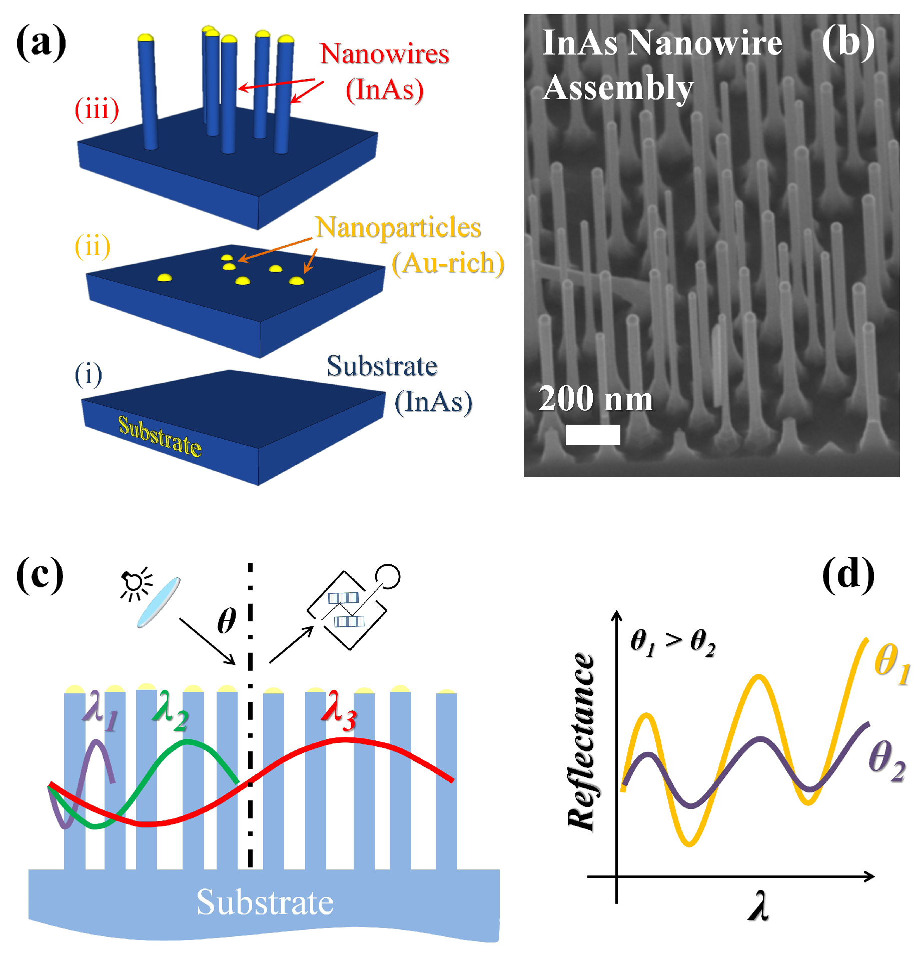
Abstract
:1. Introduction
2. Nanowire Assemblies and Light Reflection
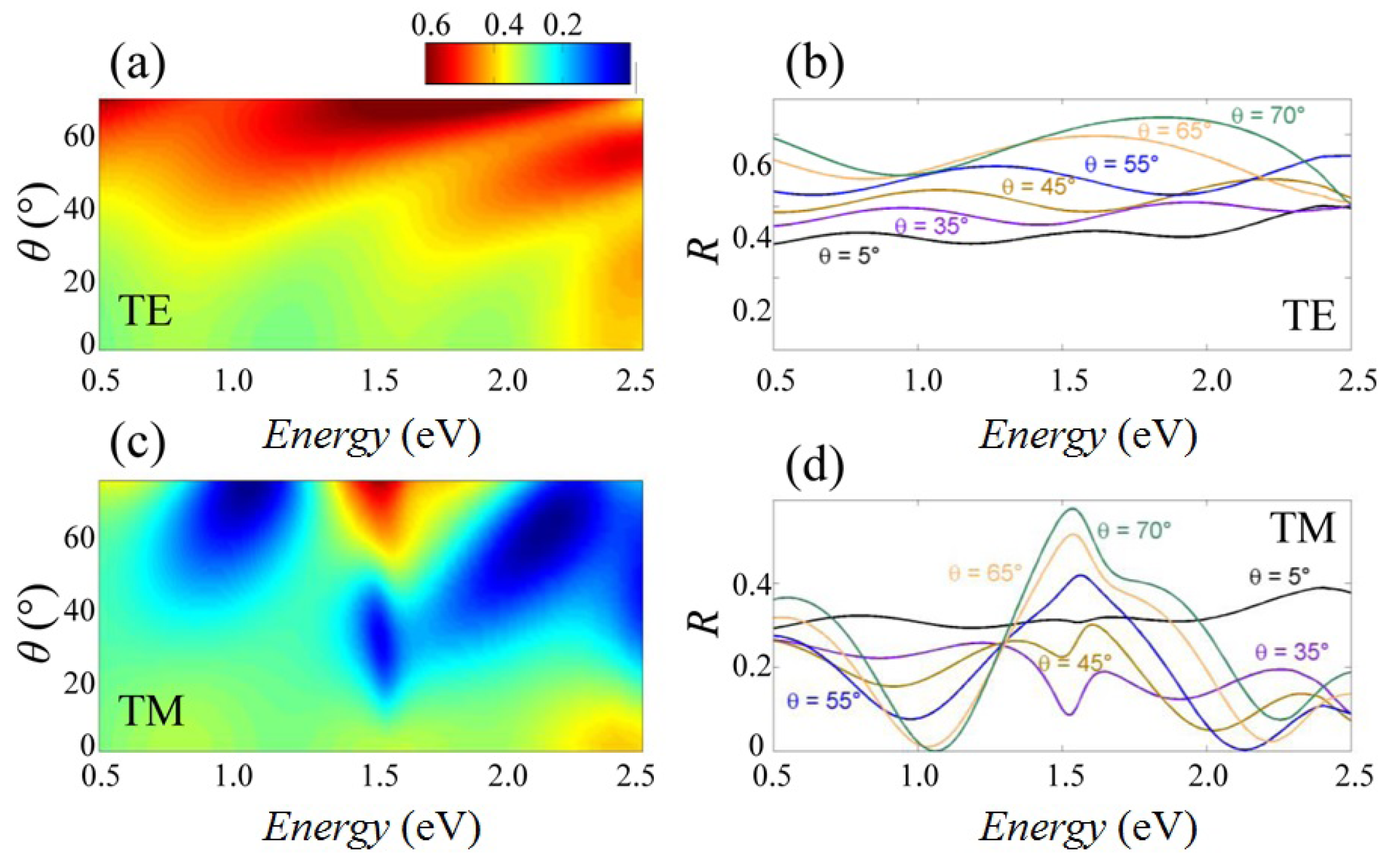
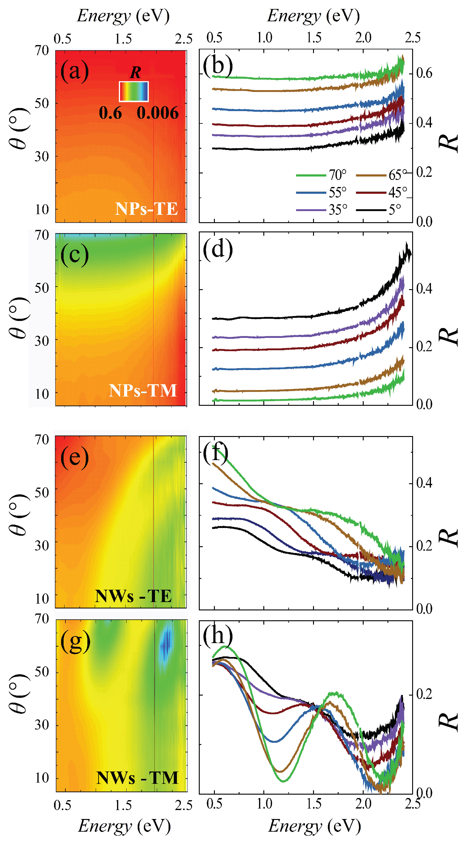
3. Experimental Results: Optical Reflectance
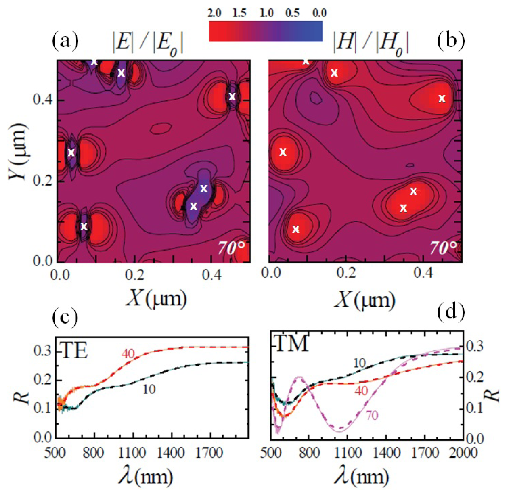
4. Theoretical Results: Analytical and Numerical Simulations
5. Discussion: Sensing Applications
6. Methods
7. Conclusions
Supplementary Materials
Acknowledgments
Author Contributions
Conflicts of Interest
References
- Yao, J.; Liu, Z.; Liu, Y.; Wang, Y.; Sun, C.; Bartal, G.; Stacy, A.M.; Zhang, X. Optical negative refraction in bulk metamaterials of nanowires. Science 2008, 321, 930. [Google Scholar] [CrossRef] [PubMed]
- Krishnamoorthy, H.N.S.; Jacob, Z.; Narimanov, E.; Kretzschmar, I.; Menon, V.M. Active hyperbolic metamaterials: Enhanced spontaneous emission and light extraction. Science 2012, 336, 205–209. [Google Scholar] [CrossRef] [PubMed]
- Noginov, M.A.; Li, H.; Barnakov, Y.A.; Dryden, D.; Nataraj, G.; Zhu, G.; Bonner, C.E.; Mayy, M.; Jacob, Z.; Narimanov, E.E. Controlling spontaneous emission with metamaterials. Opt. Lett. 2010, 35, 1863–1865. [Google Scholar] [CrossRef] [PubMed]
- Kauranen, M.; Zayats, A.V. Nonlinear plasmonics. Nat. Photonics 2012, 6, 737–748. [Google Scholar] [CrossRef]
- Belardini, A.; Centini, M.; Leahu, G.; Hooper, D.C.; Li Voti, R.; Fazio, E.; Haus, J.W.; Sarangan, A.; Valev, V.K.; Sibilia, C. Chiral light intrinsically couples to extrinsic/pseudo-chiral metasurfaces made of tilted gold nanowires. Sci. Rep. 2016, 6, 31796. [Google Scholar] [CrossRef] [PubMed]
- Lemoult, F.; Kaina, N.; Fink, M.; Lerosey, G. Wave propagation control at the deep subwavelength scale in metamaterials. Nat. Phys. 2013, 9, 55–60. [Google Scholar] [CrossRef]
- Jacob, Z.; Kim, J.Y.; Naik, G.V.; Boltasseva, A.; Narimanov, E.E.; Shalaev, V.M. Engineering photonic density of states using metamaterials. Appl. Phys. B Laser Opt. 2010, 100, 215–218. [Google Scholar] [CrossRef]
- Yu, N.; Capasso, F. Flat optics with designer metasurfaces. Nat. Mater. 2014, 13, 139–150. [Google Scholar] [CrossRef] [PubMed]
- Zhao, Y.; Alù, A. Manipulating light polarization with ultrathin plasmonic metasurfaces. Phys. Rev. B 2011, 84, 205428. [Google Scholar] [CrossRef]
- Karimi, E.; Schulz, S.A.; De Leon, I.; Qassim, H.; Upham, J.; Boyd, R.W. Generating optical orbital angular momentum at visible wavelengths using a plasmonic metasurface. Light Sci. Appl. 2014, 3, e167. [Google Scholar] [CrossRef]
- Wang, B.; Dong, F.; Li, Q.-T.; Yang, D.; Sun, C.; Chen, J.; Song, Z.; Xu, L.; Chu, W.; Xiao, Y.-F.; et al. Visible-Frequency Dielectric Metasurfaces for Multiwavelength Achromatic and Highly Dispersive Holograms. Nano Lett. 2016, 16, 5235–5240. [Google Scholar] [CrossRef] [PubMed]
- Huang, Y.-W.; Lee, H.W.H.; Sokhoyan, R.; Pala, R.A.; Thyagarajan, K.; Han, S.; Tsai, D.P.; Atwater, H.A. Gate-Tunable Conducting Oxide Metasurfaces. Nano Lett. 2016, 16, 5319–5325. [Google Scholar] [CrossRef] [PubMed]
- Yan, R.; Gargas, D.; Yang, P. Nanowire photonics. Nat. Photonics 2009, 3, 569–576. [Google Scholar] [CrossRef]
- Soldano, C.; Rossella, F.; Bellani, V.; Giudicatti, S.; Kar, S. Cobalt Nanocluster-Filled Carbon Nanotube Arrays: Engineered Photonic Bandgap and Optical Reflectivity. ACS Nano 2010, 4, 6573–6578. [Google Scholar] [CrossRef] [PubMed]
- Brongersma, M.L.; Cui, Y.; Fan, S. Light management for photovoltaics using high-index nanostructures. Nat. Mater. 2014, 13, 451–460. [Google Scholar] [CrossRef] [PubMed]
- Zhu, J.; Yu, Z.; Burkhard, G.F.; Hsu, C.-M.; Connor, S.T.; Xu, Y.; Wang, Q.; McGehee, M.; Fan, S.; Cui, Y. Optical Absorption Enhancement in Amorphous Silicon Nanowire and Nanocone Arrays. Nano Lett. 2009, 9, 279–282. [Google Scholar] [CrossRef] [PubMed]
- Garnett, E.; Yang, P. Light trapping in silicon nanowire solar cells. Nano Lett. 2010, 10, 1082–1087. [Google Scholar] [CrossRef] [PubMed]
- Wallentin, J.; Anttu, N.; Asoli, D.; Huffman, M.; Åberg, I.; Magnusson, M.H.; Siefer, G.; Fuss-Kailuweit, P.; Dimroth, F.; et al. InP nanowire array solar cells achieving 13.8% efficiency by exceeding the ray optics limit. Science 2013, 339, 1057–1060. [Google Scholar] [CrossRef] [PubMed]
- Anttu, N.; Abrand, A.; Asoli, D.; Heurlin, M.; Aberg, I.; Samuelson, L.; Borgstrom, M. Absorption of light in InP nanowire arrays. Nano Res. 2014, 7, 816–823. [Google Scholar] [CrossRef]
- LaPierre, R.R.; Chia, C.E.; Gibson, S.J.; Haapamaki, C.M.; Boulanger, J.; Yee, R.; Kuyanov, P.; Zhang, J.; Tajik, N.; Jewell, N.; et al. III-V nanowire photovoltaics: Review of design for high efficiency. Phys. Status Solidi Rapid Res. Lett. 2013, 7, 815–830. [Google Scholar] [CrossRef]
- Khorasaninejad, M.; Abedzadeh, N.; Walia, J.; Patchett, S.; Saini, S.S. Color Matrix Refractive Index Sensors Using Coupled Vertical Silicon Nanowire Arrays. Nano Lett. 2012, 12, 4228–4234. [Google Scholar] [CrossRef] [PubMed]
- Wen, L.; Li, X.; Zhao, Z.; Bu, S.; Zeng, X.; Huang, J.; Wang, Y. Theoretical consideration of III–V nanowire/Si triple-junction solar cells. Nanotechnology 2012, 23, 505202. [Google Scholar] [CrossRef] [PubMed]
- Fazio, B.; Arton, P.; Iatì, M.A.; D’Andrea, C.; Lo Faro, M.J.; Del Sorbo, S.; Pirotta, S.; Gucciardi, P.G.; Musumeci, P.; Vasi, C.S.; et al. Strongly enhanced light trapping in a two-dimensional silicon nanowire random fractal array. Light 2016, 5, e16062. [Google Scholar] [CrossRef]
- Street, R.A.; Wong, W.S.; Paulson, C. Analytic Model for Diffuse Reflectivity of Silicon Nanowire Mats. Nano Lett. 2009, 9, 3494–3497. [Google Scholar] [CrossRef] [PubMed]
- Muskens, O.L.; Diedenhofen, S.L.; van Weert, M.H.M.; Borgström, M.T.; Bakkers, E.P.A.M.; Gómez-Rivas, J. Epitaxial Growth of Aligned Semiconductor Nanowire Metamaterials for Photonic Application. Adv. Funct. Mater. 2008, 18, 1039–1046. [Google Scholar] [CrossRef]
- Muskens, O.L.; Borgström, M.T.; Bakkers, E.P.A.M.; Gómez-Rivas, J. Giant optical birefringence in ensembles of semiconductor nanowires. Appl. Phys. Lett. 2006, 89, 233117. [Google Scholar] [CrossRef]
- Gómez-Rivas, J.; Diedenhofen, S.L.; Muskens, O.L.; Grzela, G. Tailoring light scattering of nanowires for photovoltaic applications. SPIE Newsroom 2010, 10–12. [Google Scholar] [CrossRef]
- Strudley, T.; Zehender, T.; Blejean, C.; Bakkers, E.P.A.M.; Muskens, O.L. Mesoscopic light transport by very strong collective multiple scattering in nanowire mats. Nat. Photonics 2013, 7, 413–418. [Google Scholar] [CrossRef]
- Gomes, U.P.; Ercolani, D.; Zannier, V.; Beltram, F.; Sorba, L. Controlling the diameter distribution and density of InAs nanowires grown by Au-assisted methods. Semicond. Sci. Technol. 2015, 30, 115012. [Google Scholar] [CrossRef]
- Caridad, J.M.; McCloskey, D.; Rossella, F.; Bellani, V.; Donegan, J.F.; Krstić, V. Effective Wavelength Scaling of and Damping in Plasmonic Helical Antennae. ACS Photonics 2015, 2, 675–679. [Google Scholar] [CrossRef]
- Wilhelm, C.; Larrue, A.; Dai, X.; Migasd, D.; Soci, C. Anisotropic photonic properties of III–V nanowires in the zinc-blende and wurtzite phase. Nanoscale 2012, 4, 1446–1454. [Google Scholar] [CrossRef] [PubMed]
- Pollard, R.J.; Murphy, A.; Hendren, W.R.; Evans, P.R.; Atkinson, R.; Wurtz, G.A.; Zayats, A.V.; Podolskiy, V.A. Optical Nonlocalities and Additional Waves in Epsilon-Near-Zero Metamaterials. Phys. Rev. Lett. 2009, 102, 127405. [Google Scholar] [CrossRef] [PubMed]
- Giudicatti, S.; Valsesia, A.; Marabelli, F.; Colpo, P.; Rossi, F. Plasmonic resonances in nanostructured gold/polymer surfaces by colloidal lithography. Phys. Status Solidi A 2010, 4, 935–942. [Google Scholar] [CrossRef]
- Floris, F.; Figus, C.; Fornasari, L.; Patrini, M.; Pellacani, P.; Marchesini, G.; Valsesia, A.; Artizzu, F.; Marongiu, D.; Saba, M.; et al. Optical Sensitivity Gain in Silica-Coated Plasmonic Nanostructures. J. Phys. Chem. Lett. 2014, 5, 2935–2940. [Google Scholar] [CrossRef] [PubMed]
- Patolsky, F.; Lieber, C.M. Nanowire nanosensors. Mat. Today 2005, 8, 20–28. [Google Scholar] [CrossRef]
- Xu, X.; Vereecke, G.; Chen, C.; Pourtois, G.; Armini, S.; Verellen, N.; Tsai, W.-K.; Kim, D.-W.; Lee, E.; Lin, C.-Y.; et al. Capturing Wetting States in Nanopatterned Silicon. ACS Nano 2014, 8, 885–893. [Google Scholar] [CrossRef] [PubMed]
- Gwon, M.; Kim, S.; Li, J.; Xu, X.; Kim, S.-K.; Lee, E.; Kim, D.-W.; Chen, C. Influence of wetting state on optical reflectance spectra of Si nanopillar arrays. J. App. Phys. 2015, 118, 213102. [Google Scholar] [CrossRef]
- Peli, S.; Nembrini, N.; Damin, F.; Chiari, M.; Giannetti1, C.; Banfi, F.; Ferrini, G. Discrimination of molecular thin films by surface-sensitive time-resolved optical spectroscopy. Appl. Phys. Lett. 2015, 107, 163107. [Google Scholar] [CrossRef]
- Travagliati, M.; Nardi, D.; Giannetti, C.; Gusev, V.; Pingue, P.; Piazza, V.; Ferrini, G.; Banfi, F. Interface nano-confined acoustic waves in polymeric surface phononic crystals. Appl. Phys. Lett. 2015, 106, 021906. [Google Scholar] [CrossRef]
- Sackmann, E.K.; Fulton, A.L.; Beebe, D.J. The present and future role of microfluidics in biomedical research. Nature 2014, 507, 181–189. [Google Scholar] [CrossRef] [PubMed]
- Kim, J.; Junkin, M.; Kim, D.H.; Kwon, S.; Shik Shin, Y.; Kin Wong, P.; Gale, B.K. Applications, techniques, and microfluidic interfacing for nanoscale biosensing. Microfluid Nanofluid 2009, 7, 149–167. [Google Scholar] [CrossRef]
- Benetti, G.; Caddeo, C.; Melis, C.; Ferrini, G.; Giannetti, C.; Winckelmans, N.; Bals, S.; van Bael, M.J.; Cavaliere, E.; Gavioli, L.; et al. Bottom-Up Mechanical Nanometrology of Granular Ag Nanoparticles Thin Films. J. Phys. Chem. C 2017, 121, 22434–22441. [Google Scholar] [CrossRef]


© 2017 by the authors. Licensee MDPI, Basel, Switzerland. This article is an open access article distributed under the terms and conditions of the Creative Commons Attribution (CC BY) license (http://creativecommons.org/licenses/by/4.0/).
Share and Cite
Floris, F.; Fornasari, L.; Marini, A.; Bellani, V.; Banfi, F.; Roddaro, S.; Ercolani, D.; Rocci, M.; Beltram, F.; Cecchini, M.; et al. Self-Assembled InAs Nanowires as Optical Reflectors. Nanomaterials 2017, 7, 400. https://doi.org/10.3390/nano7110400
Floris F, Fornasari L, Marini A, Bellani V, Banfi F, Roddaro S, Ercolani D, Rocci M, Beltram F, Cecchini M, et al. Self-Assembled InAs Nanowires as Optical Reflectors. Nanomaterials. 2017; 7(11):400. https://doi.org/10.3390/nano7110400
Chicago/Turabian StyleFloris, Francesco, Lucia Fornasari, Andrea Marini, Vittorio Bellani, Francesco Banfi, Stefano Roddaro, Daniele Ercolani, Mirko Rocci, Fabio Beltram, Marco Cecchini, and et al. 2017. "Self-Assembled InAs Nanowires as Optical Reflectors" Nanomaterials 7, no. 11: 400. https://doi.org/10.3390/nano7110400