High-Performance and Self-Powered Deep UV Photodetectors Based on High Quality 2D Boron Nitride Nanosheets

 , , ,
, , ,
Abstract
:
1. Introduction
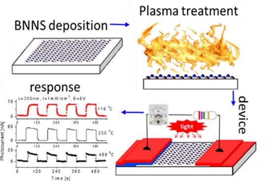
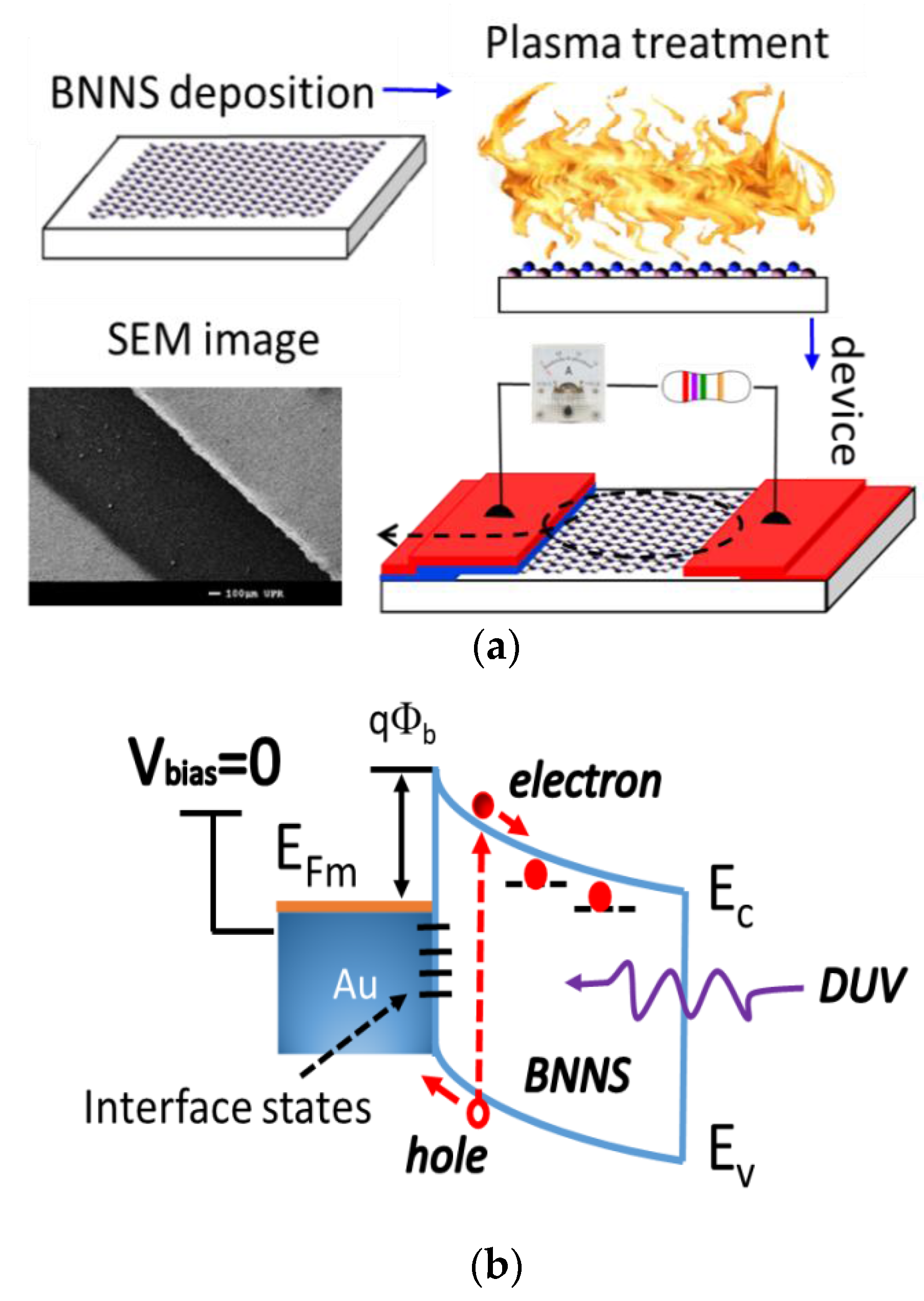
2. Experimental Section
2.1. Synthesis and Basic Characterization of BNNSs
2.2. SEM and TEM Analyses
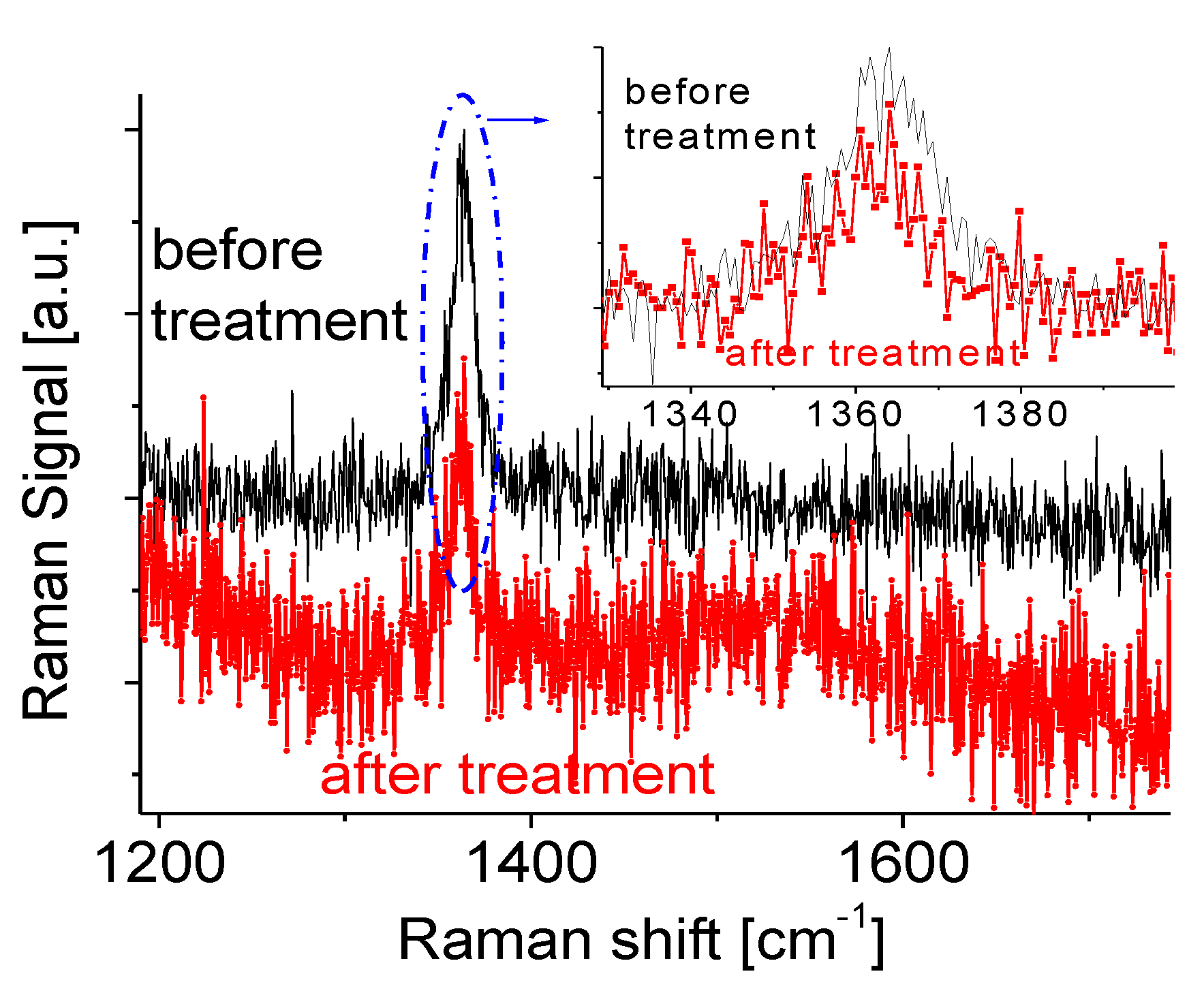
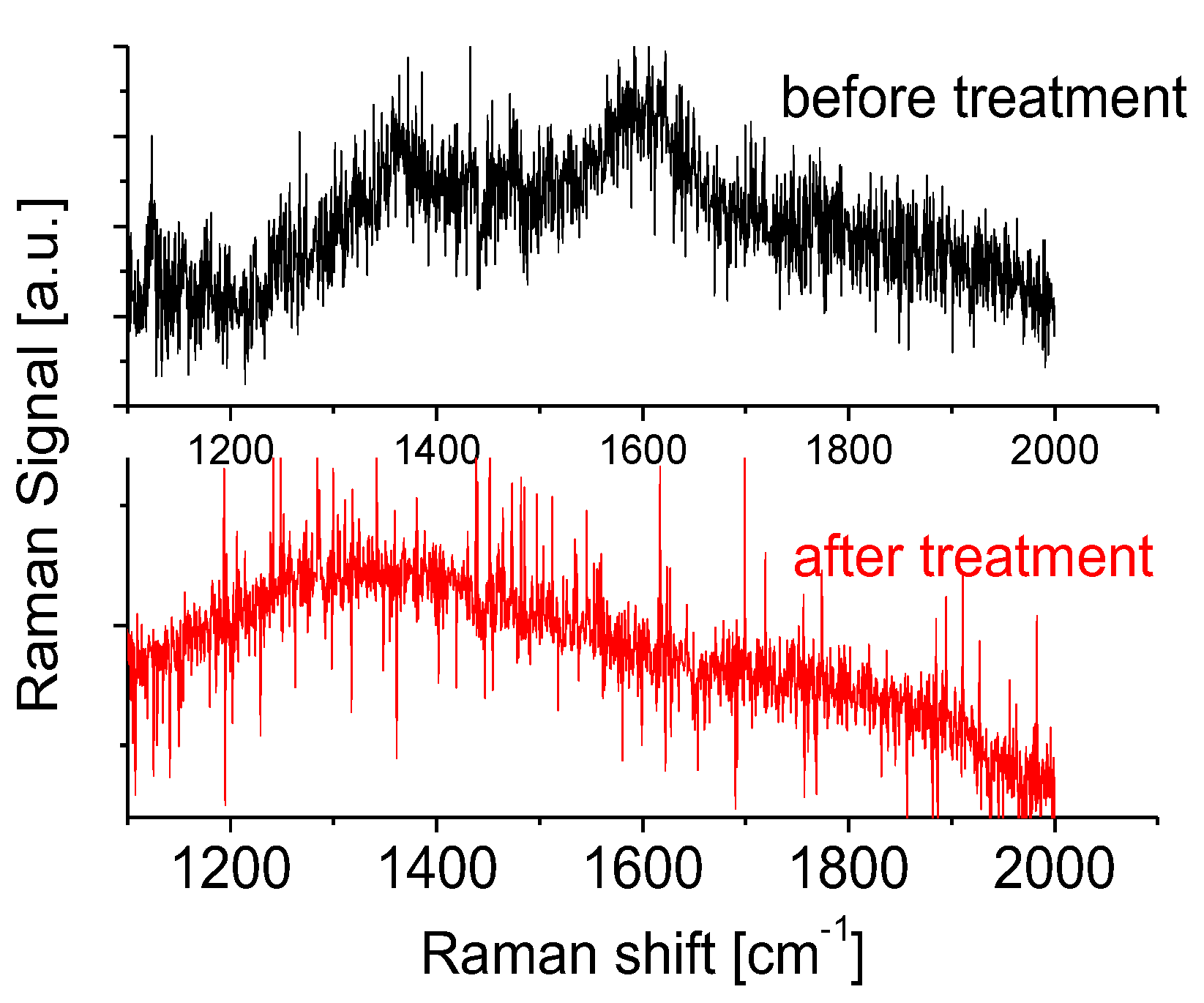
2.3. Raman Analyses
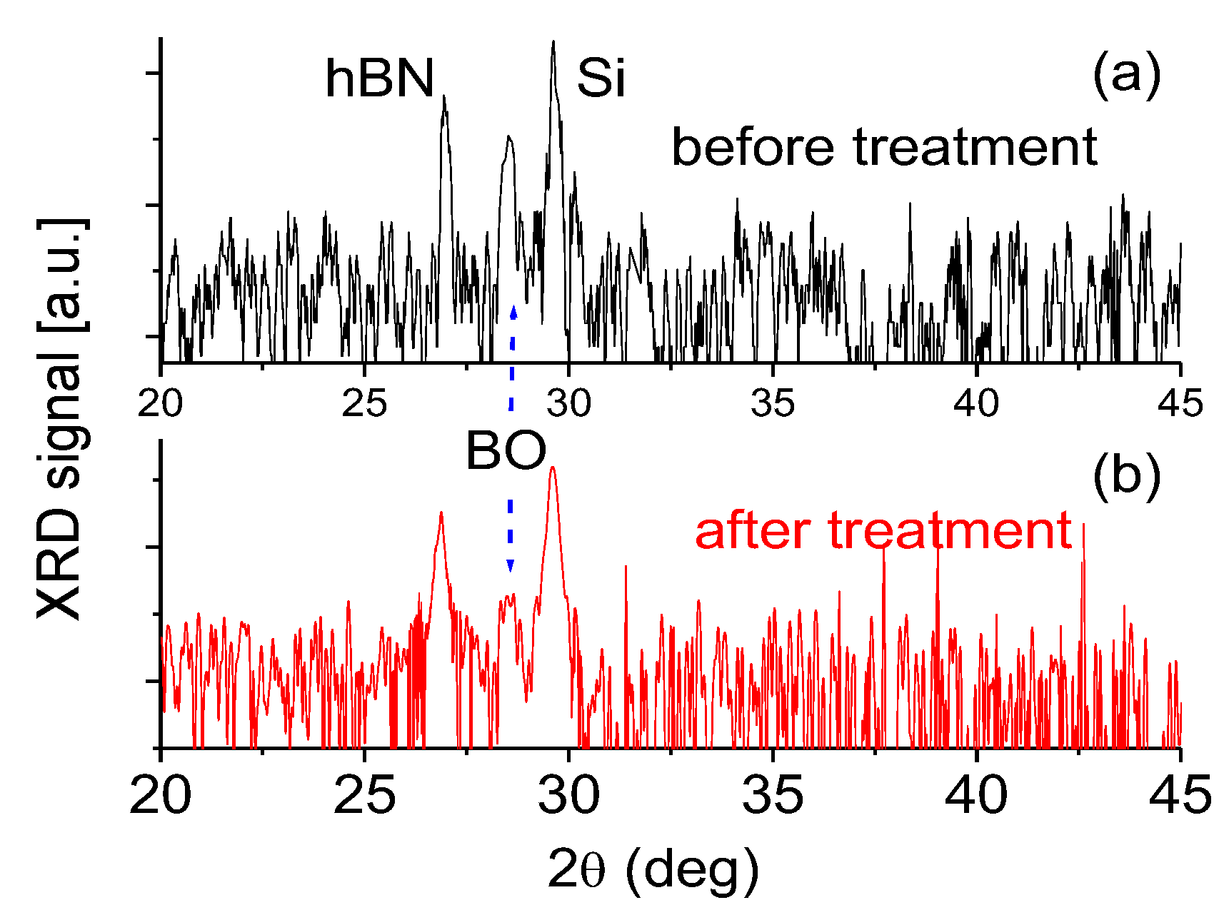
2.4. XRD Analyses
3. Results and Discussions
3.1. Fabrication of the Prototype and Characterization of Its Electrical Properties
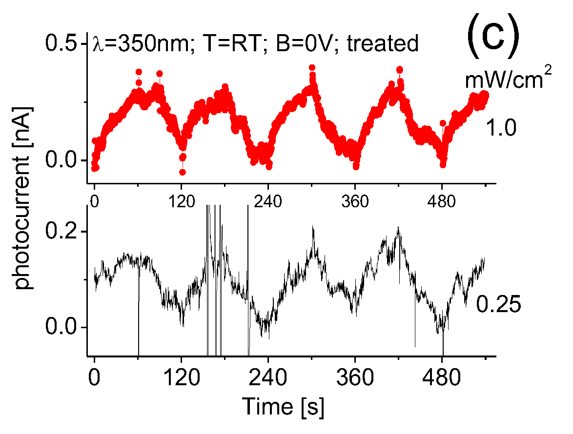
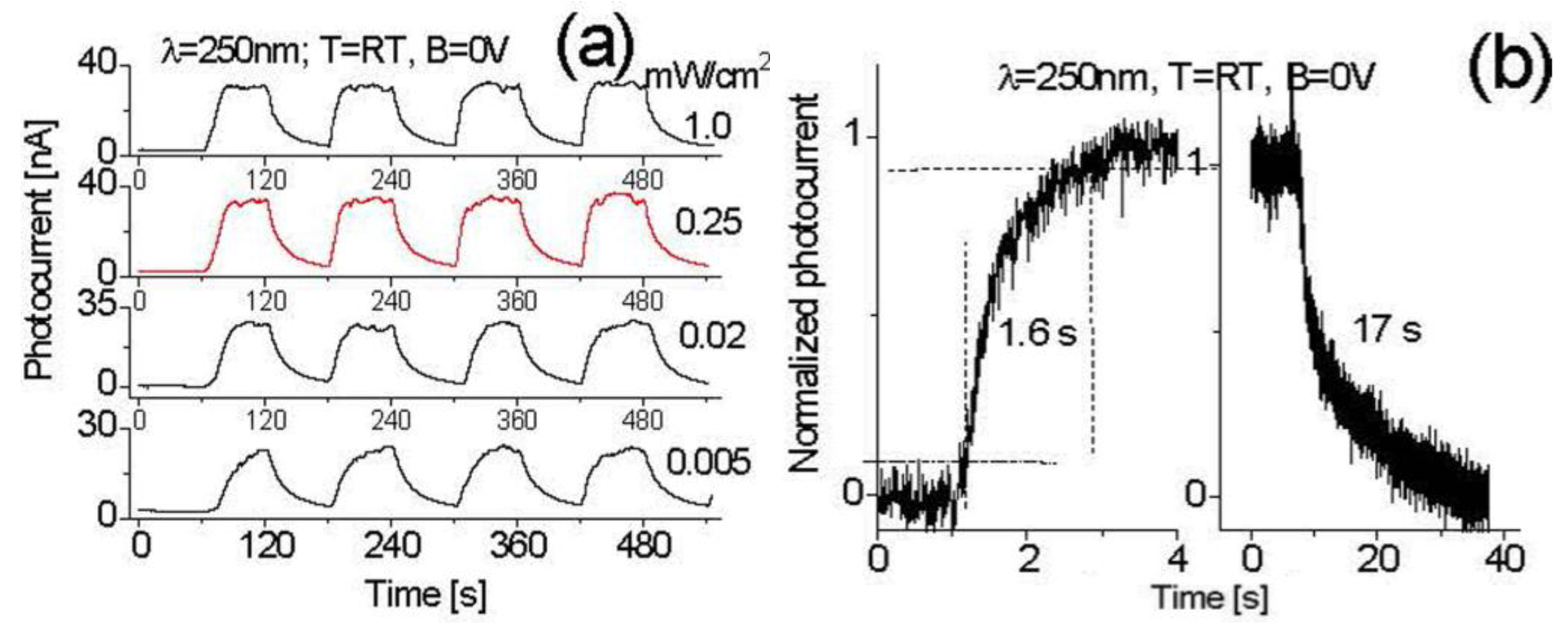
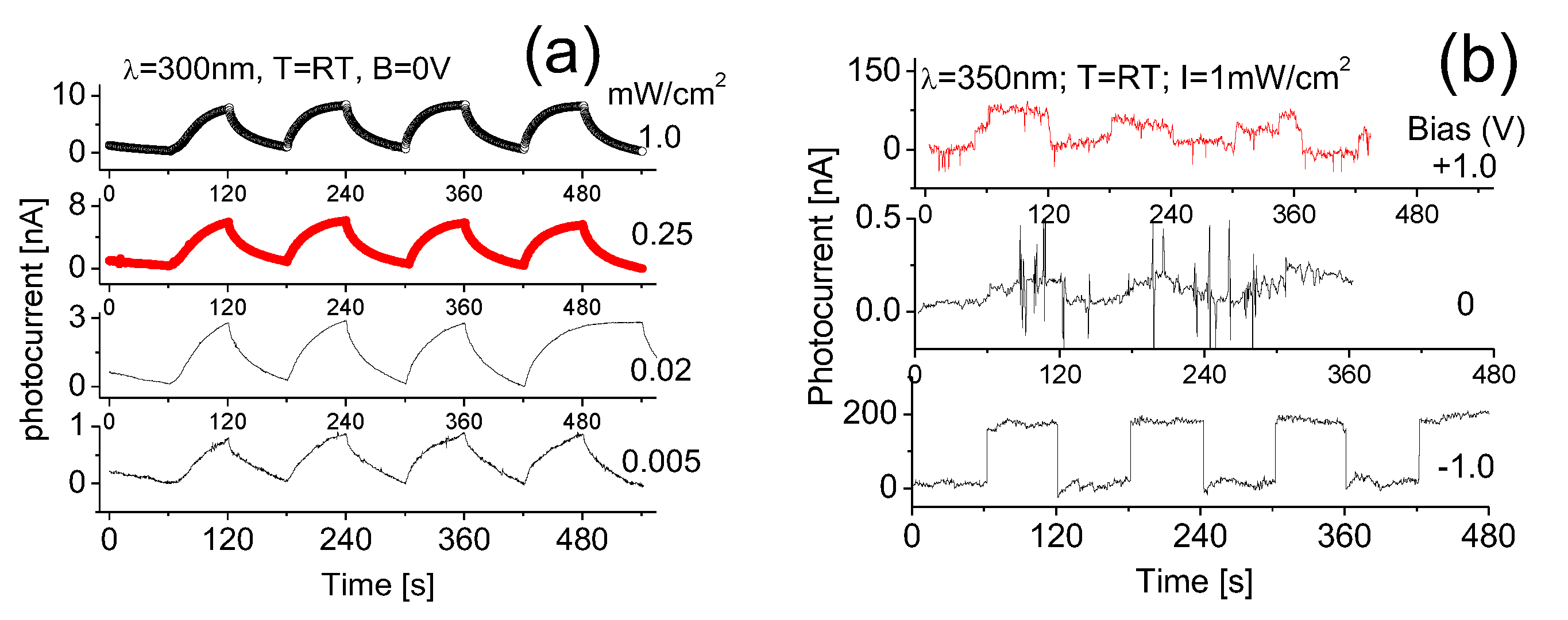
3.2. Response at Zero Bias to Various UV Wavelengths at Different Intensities
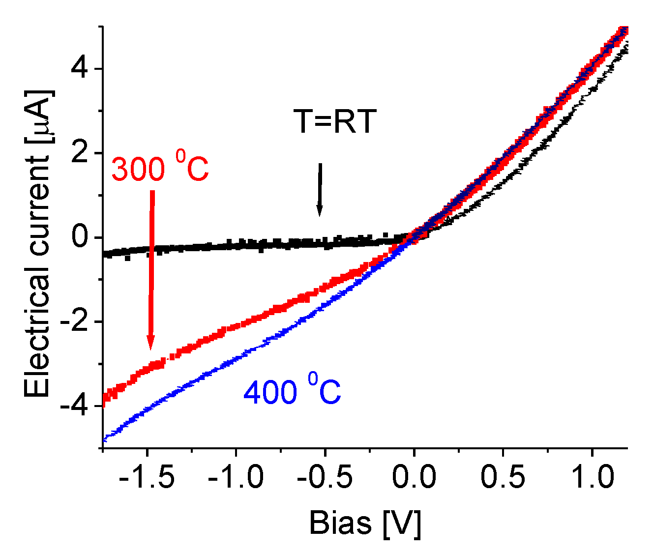
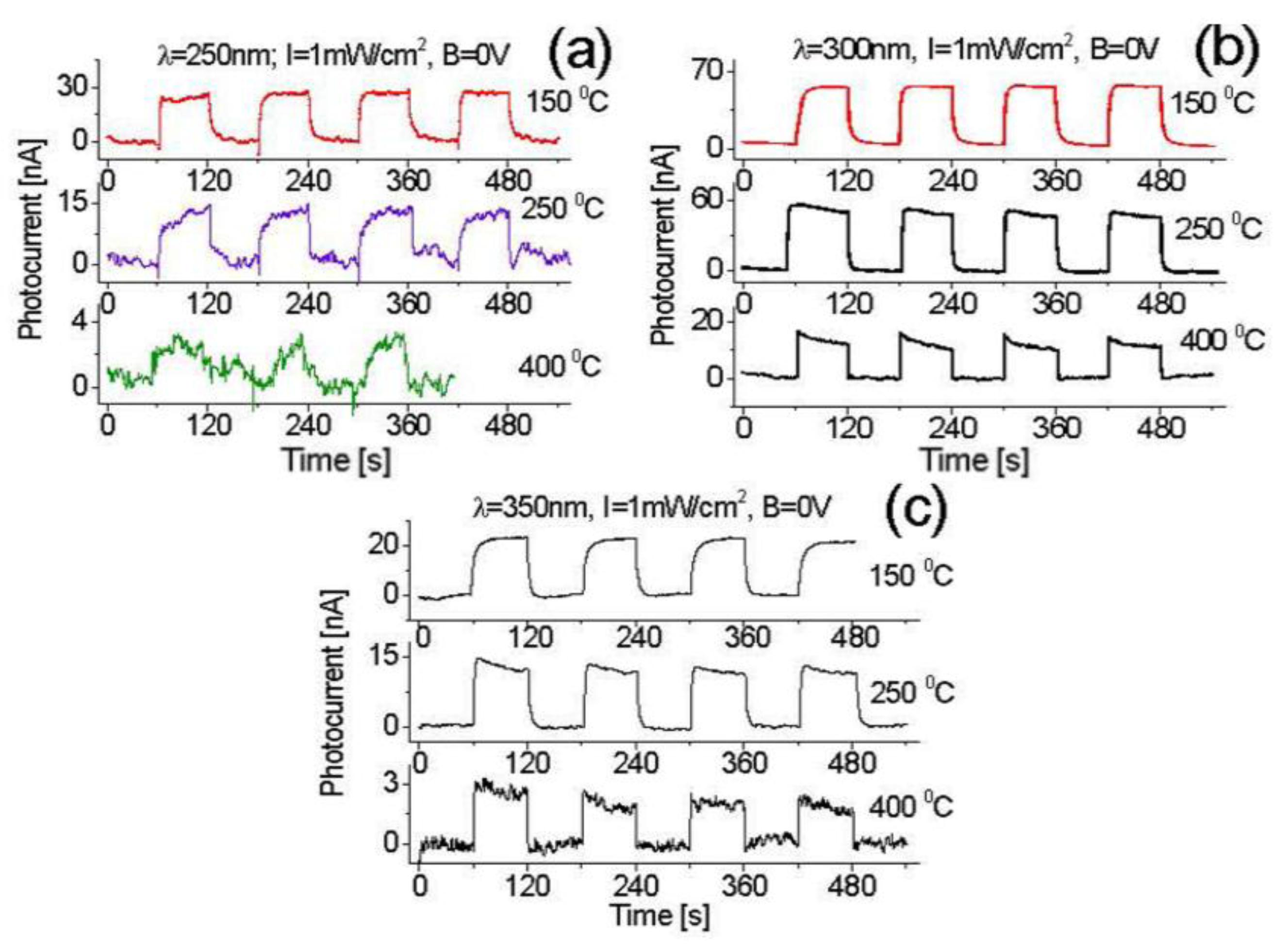
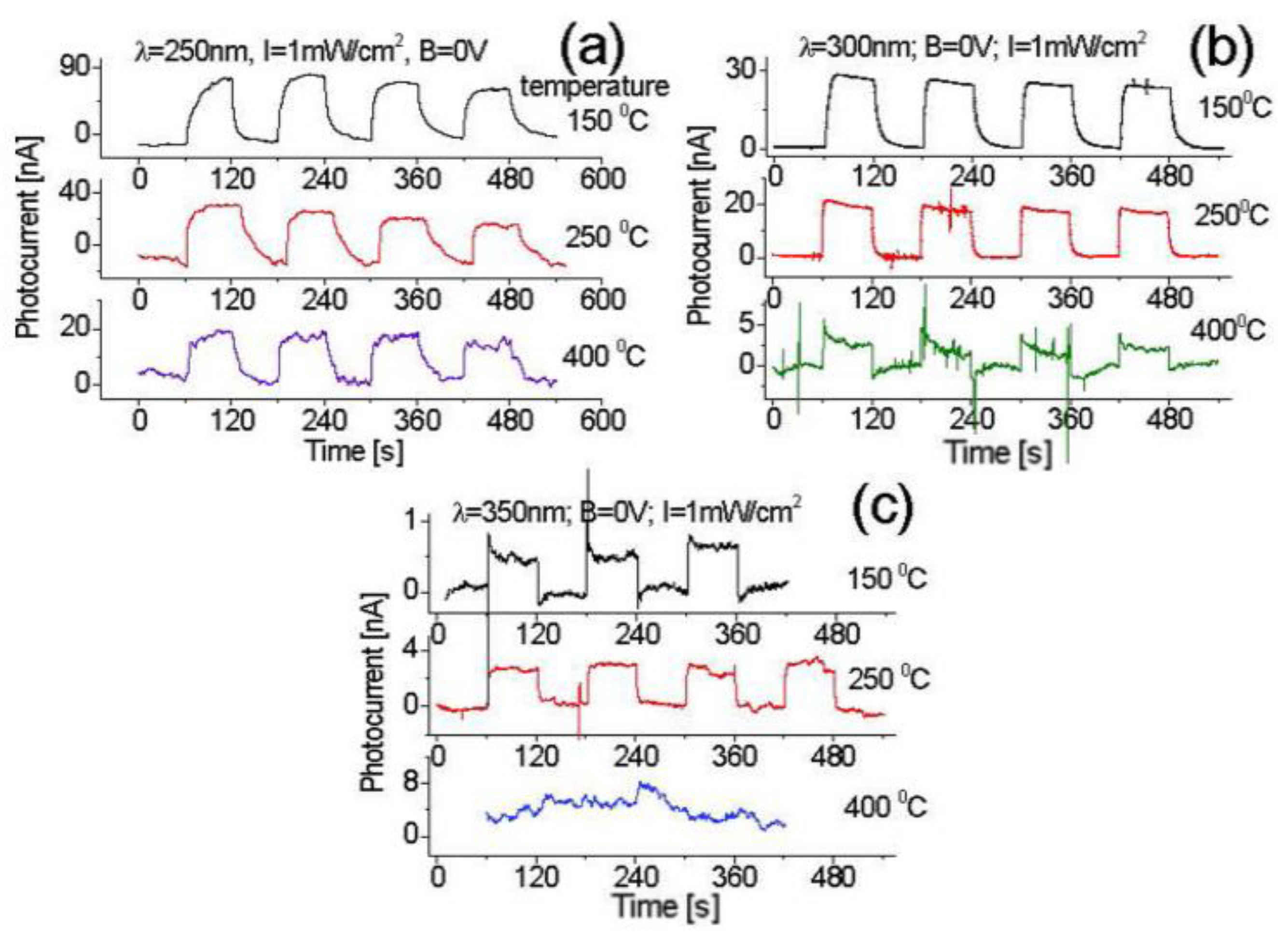
3.3. Temperature Effect
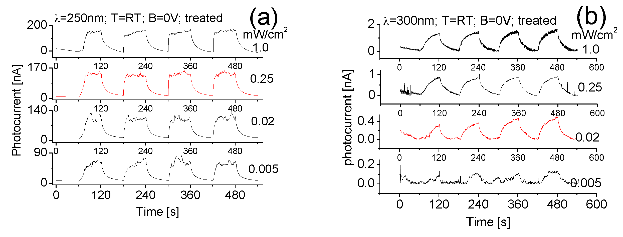
3.4. Plasma Treatment
4. Conclusions
Acknowledgments
Author Contributions
Conflicts of Interest
References
- Jiang, H.X.; Lin, J.Y. Hexagonal boron nitride for deep ultraviolet photonic devices. Semicond. Sci. Technol. 2014, 29, 84003. [Google Scholar] [CrossRef]
- Tan, C.-K.; Borovac, D.; Sun, W.; Tansu, N. Dilute-As AlNAs Alloy for Deep-Ultraviolet Emitter. Sci. Rep. 2016, 6, 22215. [Google Scholar] [CrossRef] [PubMed]
- Verma, J.; Islam, S.M.; Protasenko, V.; Kandaswamy, P.K.; Xing, H.; Jena, D. Tunnel-injection quantum dot deep-ultraviolet light-emitting diodes with polarization-induced doping in III-nitride heterostructures. Appl. Phys. Lett. 2014, 104, 021105. [Google Scholar] [CrossRef]
- Sajjad, M.; Jadwisienczak, W.M.; Feng, P. Nanoscale structure study of boron nitride nanosheets and development of deep-UV photo-detector. ACS Nanoscale 2014, 6, 4577–4582. [Google Scholar] [CrossRef] [PubMed]
- Xu, X.; Xu, C.; Hu, J. High-performance deep ultraviolet photodetectors based on ZnO quantum dot assemblies. J. Appl. Phys. 2014, 116, 103105. [Google Scholar] [CrossRef]
- Lien, W.-C.; Tsai, D.-S.; Chiu, S.-H.; Senesky, D.G.; Maboudian, R.; Pisano, A.P.; He, H., Jr. Low-temperature, ion beam-assisted SiC thin films with antireflective ZnO nanorod arrays for high-temperature photodetection. IEEE Electron Device Lett. 2011, 32, 1564–1566. [Google Scholar] [CrossRef]
- Chen, H.; Liu, K.; Hu, L.; Al-Ghamdi, A.A.; Fang, X. New concept ultraviolet photodetectors. Mater. Today 2015, 18, 493–502. [Google Scholar] [CrossRef]
- Sang, L.; Liao, M.; Sumiya, M. A comprehensive review of semiconductor ultraviolet photodetectors: From thin film to one-dimensional nanostructures. Sensors 2013, 13, 10482–10518. [Google Scholar] [CrossRef] [PubMed]
- BenMoussa, A.; Soltani, A.; Schühle, U.; Haenen, K.; Chong, Y.M.; Zhang, W.J.; Dahal, R.; Lin, J.Y.; Jiang, H.X.; Barkad, H.A.; et al. Recent developments of wide-bandgap semiconductor based UV sensors. Diam. Relat. Mater. 2009, 18, 860–864. [Google Scholar] [CrossRef]
- Goldsman, N. Silicon Carbide Electronics: Deep Ultraviolet Detectors: Design, Modeling and Fabrication. In Proceedings of the NASA Early Stage Technology Workshop: Astrophysics & Heliophysics, Crystal City, VA, USA, 3–4 March 2015. [Google Scholar]
- Omnès, F.; Monroy, E.; Muñozc, E.; Reverchond, J.-L. Wide bandgap UV photodetectors: A short review of devices and applications. In Gallium Nitride Materials and Devices II, Proceedings of the SPIE, San Jose, CA, USA, 22–25 January 2007; Morkoc, H., Litton, C.W., Eds.; SPIE: Bellingham, WA, USA, 2007. [Google Scholar]
- Alenezi, M.R.; Henley, S.J.; Silva, S.R.P. On-chip fabrication of high performance nanostructured ZnO UV detectors. Sci. Rep. 2015, 5, 8516. [Google Scholar] [CrossRef] [PubMed] [Green Version]
- Liu, Z.; Li, F.; Li, S.; Hu, C.; Wang, W.; Wang, F.; Lin, F.; Wang, H. Fabrication of UV photodetector on TiO2/diamond film. Sci. Rep. 2015, 5, 14420. [Google Scholar] [CrossRef] [PubMed]
- Velazquez, R.; Aldalbahi, A.; Rivera, M.; Feng, P. Fabrications and application of single crystalline GaN for high-performance DUV photodetectors. AIP Adv. 2016, 6, 85117. [Google Scholar] [CrossRef]
- Laksana, C.; Chen, M.R.; Liang, Y.; Tzou, A.J.; Kao, H.L.; Jeng, E.; Chen, J.; Chen, H.G.; Jian, S.R. Deep-UV sensors based on SAW oscillators using low-temperature-grown AlN films on sapphires. IEEE Trans. Ultrason. Ferroelectr. Freq. Control 2011, 58, 1688–1693. [Google Scholar] [CrossRef] [PubMed]
- Dahal, R.; Li, J.; Majety, S.; Pantha, B.N.; Cao, X.K.; Lin, J.Y.; Jiang, H.X. Epitaxially grown semiconducting hexagonal boron nitride as a deep ultraviolet photonic material. Appl. Phys. Lett. 2011, 98, 211110. [Google Scholar] [CrossRef]
- Aldalbahi, A.; Li, E.; Rivera, M.; Velazquez, R.; Altalhi, T.; Peng, X.; Feng, P. A new approach for fabrications of SiC based photodetectors. Sci. Rep. 2016, 6, 23457. [Google Scholar] [CrossRef] [PubMed]
- Lin, C.R.; Wei, D.H.; BenDao, M.K.; Chen, W.E.; Liu, T.Y. Development of High-Performance UV Detector Using Nanocrystalline Diamond Thin Film. Int. J. Photoenergy 2014, 2014, 1–8. [Google Scholar] [CrossRef]
- Pace, E.; De Sio, A. Innovative diamond photo-detectors for UV astrophysics. Memorie della Società Astronomica Italiana Supplement 2010, 14, 84–89. [Google Scholar]
- Li, C.; Bando, Y.; Liao, M.; Koide, Y.; Golberg, D. Visible-blind deep-ultraviolet Schottky photodetector with a photocurrent gain based on individual Zn2GeO4Zn2GeO4 nanowire. Appl. Phys. Lett. 2010, 97, 161102. [Google Scholar] [CrossRef]
- Li, L.; Lee, P.S.; Yan, C.; Zhai, T.; Fang, X.; Liao, M.; Koide, Y.; Bando, Y.; Golberg, D. Ultrahigh-Performance Solar-Blind Photodetectors Based on Individual Single-crystalline In2Ge2O7 Nanobelts. Adv. Mater. 2010, 22, 5145. [Google Scholar] [CrossRef] [PubMed]
- Jiang, X.-F.; Weng, Q.; Wang, X.-B.; Li, X.; Zhang, J.; Golberg, D.; Bando, Y. Recent Progress on Fabrications and Applications of Boron Nitride Nanomaterials: A Review. J. Mater. Sci. Technol. 2015, 31, 589–598. [Google Scholar] [CrossRef]
- Rivera, M.; Velázquez, R.; Aldalbahi, A.; Zhou, A.F.; Feng, P. High Operating Temperature and Low Power Consumption Boron Nitride Nanosheets Based Broadband UV Photodetector. Sci. Rep. 2017, 7, 42973. [Google Scholar] [CrossRef] [PubMed]
- Aldalbahi, A.; Feng, P. Development of 2D boron nitride nanosheets UV photoconductive detectors. IEEE Trans. Electron Devices 2015, 62, 1885. [Google Scholar] [CrossRef]
- Li, J.; Majety, S.; Dahal, R.; Zhao, W.P.; Lin, J.Y.; Jiang, H.X. Dielectric strength, optical absorption, and deep ultraviolet detectors of hexagonal boron nitride epilayers. Appl. Phys. Lett. 2012, 101, 171112. [Google Scholar] [CrossRef]
- Yu, J.; Qin, L.; Hao, Y.; Kuang, S.; Bai, X.; Chong, Y.-M.; Zhang, W.; Wang, E. Vertically aligned boron nitride nanosheets: Chemical vapor synthesis, ultraviolet light emission, and super hydrophobicity. ACS Nano 2010, 4, 414. [Google Scholar] [CrossRef] [PubMed]
- Zou, R.; Zhang, Z.; Liu, Q.; Hu, J.; Sang, L.; Liao, M.; Zhang, W. High Detectivity Solar-Blind High-Temperature Deep-UV Photodetector Based on Multi-Layered (l00) Facet-Oriented β-Ga2O3 Nanobelts. Small 2014, 10, 1848–1856. [Google Scholar] [CrossRef] [PubMed]
- Chang, W.-R.; Fang, Y.-K.; Ting, S.-F.; Tsair, Y.-S.; Chang, C.-N.; Lin, C.-Y.; Chen, S.-F. The hetero-epitaxial SiCN/Si MSM photodetector for high-temperature deep-UV detecting applications. IEEE Electron Device Lett. 2003, 24, 565–567. [Google Scholar] [CrossRef]
- Zhang, S.; Lian, G.; Si, H.; Wang, J.; Zhang, X.; Wang, Q.; Cui, D. Ultrathin BN nanosheets with zigzag edge: One-step chemical synthesis, applications in wastewater treatment and preparation of highly thermal-conductive BN–polymer composites. J. Mater. Chem. A 2013, 1, 5105–5112. [Google Scholar] [CrossRef]
- Khan, M.H.; Huang, Z.; Xiao, F.; Casillas, G.; Chen, Z.; Molino, P.J.; Liu, H.K. Synthesis of large and few atomic layers of hexagonal boron nitride on melted copper. Sci. Rep. 2015, 5, 7743. [Google Scholar] [CrossRef] [PubMed]
- Wang, X.; Zhi, C.; Li, L.; Zeng, H.; Li, C.; Mitome, M.; Golberg, D.; Bando, Y. Chemical blowing of thin-walled bubbles: High-throughput fabrication of large-area, few-layered BN and Cx-BN Nanosheets. Adv. Mater. 2011, 23, 4072. [Google Scholar] [CrossRef] [PubMed]
- Du, M.; Wu, Y.; Hao, X. A facile chemical exfoliation method to obtain large size boron nitride Nanosheets. CrystEngComm 2013, 15, 1782. [Google Scholar] [CrossRef]
- Wang, Y.; Shi, Z.; Yin, J. Boron nitride nanosheets: large-scale exfoliation in methanesulfonic acid and their composites with polybenzimidazole. J. Mater. Chem. 2011, 21, 11371. [Google Scholar] [CrossRef]
- Deepika; Li, L.H.; Glushenkov, A.M.; Hait, S.K.; Hodgson, P.; Chen, Y. High-efficient production of boron nitride nanosheets via an optimized ball milling process for lubrication in oil. Sci. Rep. 2014, 4, 7288. [Google Scholar] [CrossRef] [PubMed]
- Lee, C.; Li, Q.; Kalb, W.; Liu, X.-Z.; Berger, H.; Carpick, R.W.; Hone, J. Frictional characteristics of atomically thin sheets. Science 2010, 328, 76–80. [Google Scholar] [CrossRef] [PubMed]
- Zhi, C.; Bando, Y.; Tang, C.; Kuwahara, H.; Golberg, D. Large-scale fabrication of boron nitride nanosheets and their utilization in polymeric composites with improved thermal and mechanical properties. Adv. Mater. 2009, 21, 2889. [Google Scholar] [CrossRef]
- Lei, W.; Potehauh, D.; Liu, D.; Qin, S.; Chen, Y. Porous boron nitride nanosheets for effective water cleaning. Nat. Commun. 2013, 4, 1777. [Google Scholar] [CrossRef] [PubMed]
- Sajjad, M.; Peng, X.; Chu, J.; Zhang, H.; Feng, P. Design and installation of a CO2-pulsed laser plasma deposition system for the growth of mass product nanostructures. J. Mater. Res. 2013, 28, 1747–1752. [Google Scholar] [CrossRef]
- Feng, P.; Li, E.Y.; Sajjad, M.; Aldalbahi, A.; Chu, J. Boron Nitride Nanosheets and Their Electrical Tunneling Effect. Sci. Adv. Mater. 2015, 7, 1326. [Google Scholar] [CrossRef]
- Sajjad, M.; Morell, G.; Feng, P. Advance in Novel Boron Nitride Nanosheets to Nanoelectronic Device Applications. ACS Appl. Mater. Interfaces 2013, 5, 5051–5056. [Google Scholar] [CrossRef] [PubMed]
- Sajjad, M.; Ahmadi, M.; Guinel, M.J.-F.; Lin, Y.; Feng, P. Large-scale synthesis of single-crystal and polycrystalline boron nitride nanosheets. J. Mater. Sci. 2013, 48, 2543–2549. [Google Scholar] [CrossRef]
- Chen, H.; Yu, P.; Zhang, Z.; Teng, F.; Zheng, L.; Hu, K.; Fang, X. Ultrasensitive Self-Powered Solar-Blind Deep-Ultraviolet Photodetector Based on All-Solid-State Polyaniline/MgZnO Bilayer. Small 2016, 12, 5809–5816. [Google Scholar] [CrossRef] [PubMed]
- Lin, P.; Yan, X.; Zhang, Z.; Shen, Y.; Zhao, Y.; Bai, Z.; Zhang, Y. Self-Powered UV Photosensor Based on PEDOT:PSS/ZnO Micro/Nanowire with Strain-Modulated Photoresponse. ACS Appl. Mater. Interfaces 2013, 5, 3671–3676. [Google Scholar] [CrossRef] [PubMed]
- Zu, X.; Wang, H.; Yi, G.; Zhang, Z.; Jiang, X.; Gong, J.; Luo, H. Self-powered UV photodetector based on heterostructured TiO2 nanowire arrays and polyaniline nanoflower arrays. Synth. Met. 2015, 200, 58–65. [Google Scholar] [CrossRef]
- Xie, Y.; Wei, L.; Li, Q.; Chen, Y.; Yan, S.; Jiao, J.; Liu, G.; Mei, L. High-performance self-powered UV photodetectors based on TiO2 nano-branched arrays. Nanotechnology 2014, 25, 075202. [Google Scholar] [CrossRef] [PubMed]
- Prakash, N.; Singh, M.; Kumar, G.; Barvat, A.; Anand, K.; Pal, P.; Singh, S.P.; Khanna, S.P. Ultrasensitive Self-powered large area planar GaN UV-photodetector using reduced graphene oxide electrodes. Appl. Phys. Lett. 2016, 109, 242102. [Google Scholar] [CrossRef]
- Chen, X.; Liu, K.; Zhang, Z.; Wang, C.; Li, B.; Zhao, H.; Zhao, D.; Shen, D. Self-Powered Solar-Blind Photodetector with Fast Response Based on Au/β-Ga2O3 Nanowires Array Film Schottky Junction. ACS Appl. Mater. Interfaces 2016, 8, 4185–4191. [Google Scholar] [CrossRef] [PubMed]
- Yang, Y.; Guo, W.; Qi, J.; Zhao, J.; Zhang, Y. Self-powered ultraviolet photodetector based on a single Sb-doped ZnO nanobelt. Appl. Phys. Lett. 2010, 97, 223113. [Google Scholar] [CrossRef]
- Lee, B.; Kim, C.; Lee, Y.; Lee, S.; Kim, D.Y. Dependence of photocurrent on UV wavelength in ZnO/Pt bottom-contact Schottky diode. Curr. Appl. Phys. 2015, 15, 29. [Google Scholar] [CrossRef]
- Kumar, A.; Latzel, M.; Christiansen, S.; Kumar, V.; Singh, R. Effect of rapid thermal annealing on barrier height and 1/f noise of Ni/GaN Schottky barrier diodes. Appl. Phys. Lett. 2015, 107, 093502. [Google Scholar] [CrossRef]
- Chawanda, A.; Coelho, S.M.M.; Auret, F.D.; Mtangi, W.; Nyamhere, C.; Nel, J.M.; Diale, M. Effect of thermal treatment on the characteristics of iridium Schottky barrier diodes on n-Ge (1 0 0). J. Alloys Compd. 2012, 513, 44. [Google Scholar] [CrossRef]
- Doan, T.C.; Li, J.; Lin, J.Y.; Jiang, H.X. Charge carrier transport properties in layer structured hexagonal boron nitride. AIP Adv. 2014, 4, 107126. [Google Scholar] [CrossRef]
- He, B.; Qiu, M.; Yuen, M.F.; Zhang, W.J. Electrical properties and electronic structure of Si-implanted hexagonal boron nitride films. Appl. Phys. Lett. 2014, 105, 012104. [Google Scholar] [CrossRef]
- Zhang, Z.; Guo, W.; Yakobson, B.I. Self-modulated band gap in boron nitride nanoribbons and hydrogenated sheets. Nanoscale 2013, 5, 6381–6387. [Google Scholar] [CrossRef] [PubMed]
- Park, C.-H.; Louie, S.G. Energy gaps and stark effect in boron nitride nanoribbons. Nano Lett. 2008, 8, 2200–2203. [Google Scholar] [CrossRef] [PubMed]
- Kang, J.; Zhang, L.; Wei, S.H. A Unified Understanding of the Thickness-Dependent Bandgap Transition in Hexagonal Two-Dimensional Semiconductors. J. Phys. Chem. Lett. 2016, 7, 597–602. [Google Scholar] [CrossRef] [PubMed]
- Zeng, H.; Zhi, C.; Zhang, Z.; Wei, X.; Wang, X.; Guo, W.; Bando, Y.; Golberg, D. White graphenes: Boron nitride nanoribbons via boron nitride nanotube unwrapping. Nano Lett. 2010, 10, 5049–5055. [Google Scholar] [CrossRef] [PubMed]
- Yamijala, S.S.R.K.C.; Pati, S.K. Effects of edge passivations on the electronic and magnetic properties of zigzag boron-nitride nanoribbons with even and odd-line stone-wales (5–7 pair) defects. Indian J. Phys. 2014, 88, 931–938. [Google Scholar] [CrossRef]
- Qi, J.; Qian, X.; Qi, L.; Feng, J.; Shi, D.; Ju, L. Strain-engineering of band gaps in piezoelectric boron nitride nanoribbons. Nano Lett. 2012, 12, 1224–1228. [Google Scholar] [CrossRef] [PubMed]
- Koswattage, K.R.; Shimoyama, I.; Baba, Y.; Sekiguchi, T.; Nakagawa, K. Selective adsorption of atomic hydrogen on a h-BN thin film. J. Chem. Phys. 2011, 135, 014706. [Google Scholar] [CrossRef] [PubMed]
- Zhang, H.X.; Feng, P.X. Controlling bandgap of rippled hexagonal boron nitride membranes via plasma treatment. ACS Appl. Mater. Interfaces 2012, 4, 30–33. [Google Scholar] [CrossRef] [PubMed]
- Feng, P.; Sajjad, M.; Li, E.Y.; Zhang, H.; Chu, J.; Aldalbahi, A.; Morell, G. Fringe structures and tunable bandgap width of 2D boron nitride Nanosheets. Beilstein J. Nanotechnol. 2014, 5, 1186–1192. [Google Scholar] [CrossRef] [PubMed]
- Mendoza, F.; Makarov, V.; Hildalgo, A.; Weiner, B.; Morell, G. Solar-blind field-emission diamond ultraviolet detector. J. Appl. Phys. 2011, 109, 114904. [Google Scholar] [CrossRef]


| T = RT, before plasma treatment | |||||
| I (mW/cm2) | 1 | 0.25 | 0.02 | 0.005 | |
| Light (λ) | |||||
| 250 nm | 34 nA | 33 nA | 29 nA | 23 nA | |
| 300 nm | 9 nA | 5.5 nA | 2.7 nA | 0.8 nA | |
| 350 nm | 0.14 nA | - | - | - | |
| I = 1 mW/cm2, before plasma treatment | |||||
| T (°C) | RT | 150 | 250 | 400 | |
| Light (λ) | |||||
| 250 nm | 34 nA | 30 nA | 14 nA | 2.7 nA | |
| 300 nm | 9 nA | 56.8 nA | 53 nA | 14.2 nA | |
| 350 nm | 0.14 nA | 22.4 nA | 12.2 nA | 2.2 nA | |
| T = RT, after plasma treatment | |||||
| I (mW/cm2) | 1 | 0.25 | 0.02 | 0.005 | |
| Light (λ) | |||||
| 250 nm | 162.7 nA | 139 nA | 105 nA | 67 nA | |
| 300 nm | 1.5 nA | 0.85 nA | 0.53 nA | 0.11 nA | |
| 350 nm | 0.33 nA | 0.18 nA | - | - | |
| I = 1 mW/cm2, after plasma treatment | |||||
| T (°C) | RM | 150 | 250 | 400 | |
| Light (λ) | |||||
| 250 nm | 162.7 nA | 81 nA | 29 nA | 18 nA | |
| 300 nm | 1.5 nA | 26 nA | 17.8 nA | 2.4 nA | |
| 350 nm | 0.33 nA | 0.64 nA | 2.9 nA | - | |
© 2017 by the authors. Licensee MDPI, Basel, Switzerland. This article is an open access article distributed under the terms and conditions of the Creative Commons Attribution (CC BY) license (http://creativecommons.org/licenses/by/4.0/).
Share and Cite
Aldalbahi, A.; Rivera, M.; Rahaman, M.; Zhou, A.F.; Mohammed Alzuraiqi, W.; Feng, P. High-Performance and Self-Powered Deep UV Photodetectors Based on High Quality 2D Boron Nitride Nanosheets. Nanomaterials 2017, 7, 454. https://doi.org/10.3390/nano7120454
Aldalbahi A, Rivera M, Rahaman M, Zhou AF, Mohammed Alzuraiqi W, Feng P. High-Performance and Self-Powered Deep UV Photodetectors Based on High Quality 2D Boron Nitride Nanosheets. Nanomaterials. 2017; 7(12):454. https://doi.org/10.3390/nano7120454
Chicago/Turabian StyleAldalbahi, Ali, Manuel Rivera, Mostafizur Rahaman, Andrew F. Zhou, Waleed Mohammed Alzuraiqi, and Peter Feng. 2017. "High-Performance and Self-Powered Deep UV Photodetectors Based on High Quality 2D Boron Nitride Nanosheets" Nanomaterials 7, no. 12: 454. https://doi.org/10.3390/nano7120454