Pure and Highly Nb-Doped Titanium Dioxide Nanotubular Arrays: Characterization of Local Surface Properties


1
Institute of Electronics, Silesian University of Technology, 44-100 Gliwice, Poland
2
Sensor Lab., Department of Information Engineering, University of Brescia, 25133 Brescia, Italy
*
Author to whom correspondence should be addressed.
Nanomaterials 2017, 7(12), 456; https://doi.org/10.3390/nano7120456
Submission received: 16 October 2017
/
Revised: 11 December 2017
/
Accepted: 15 December 2017
/
Published: 18 December 2017
Abstract
:This paper presents the results of studies of the local surface properties of pure and highly Nb-doped (12 wt %) TiO2 nanotubes (TNT) using the X-ray photoelectron spectroscopy (XPS) and scanning electron microscopy (SEM) methods, respectively. XPS analysis showed that the pure TNT exhibit an evident over-stoichiometry combined with high level of undesired C contaminations, which was confirmed by the relative concentration of specific elements O, Ti and C (with respect to all the surface atoms) equal to 0.46, 018 and 0.36, respectively. In turn, for the highly Nb-doped (12 wt %) TNT, a slightly different surface chemistry was observed because the relative concentration of specific elements O and Ti and, with respect to all the surface atoms, is slightly lower, that is, 0.42 and 0.12, respectively; this is directly related to the fact that Nb atoms appeared having the relative concentration at the level of 0.09, whereas the undesired C contaminations reached the same level (0.36), as is the case of pure TNT. In addition, SEM analysis confirms that there are evident free spaces between the specific slops containing several TNT, what was additionally confirmed by the contribution of specific surface bonding coming from the SiO2/Si substrate. The obtained information allowed us a new insight on the potential origin of aging effect at the surface of TNT in atmosphere being the undesired limitation for their potential application as the chemical resistive type sensors or in any other fields of their application related to their surface activity.
1. Introduction
In the last several years there was an increasing attention of the scientific community to titanium dioxide (TiO2), an n-type wide band-gap stable nontoxic oxide semiconductor material, exhibiting extraordinary physical, chemical, electronic, electrochemical and photoactive properties. This was among the reasons that TiO2 has been found to be a very important electronic material for potential application in photovoltaics [1,2,3], photocatalysis [4,5], and chemical/gas sensing [6,7,8,9,10].
It is well known that TiO2 based gas sensors are particularly attractive for the detection of reducing gases, and that larger surface to volume ratio provides better gas sensing performances [11]. This is why special attention was given to the different forms of nanostructures having large specific surface area. In particular, hierarchical nanostructured TiO2 seems to be among the best candidates for the development of gas sensors because its conductance/resistance changes with the surface adsorption and desorption of gas molecules in a reversible way. This is related to the electronic transfer that occurs between the chemical species and the semiconductor upon the molecules adsorption over the surface [12].
Because the conductance change strongly depend on the nanostructures shape and size, nanostructured titania with tubular shape seems to be one of the most promising materials for the fabrication of novel type gas sensing devices [13].
Lately it was also recognized that anatase phase of TiO2 is more reactive than the rutile phase [14]. Thus, in order to enhance TiO2 sensor properties the phase transformation from anatase to rutile should be avoided, stabilizing the anatase phase even at higher temperatures and hindering its transition to rutile observed already at ~600 °C.
It is also well known that addition of pentavalent atoms like Nb or Ta to titania evidently diminishes the anatase to rutile transformation and also hinders the grain growth [15]. This is extremely important because the addition of different metals as dopants to the metal oxides lattice cause the enhancement of their gas sensing performances (sensitivity, selectivity, response time, etc.) [16].
The most popular methods for the synthesis of one-dimensional TiO2 nanostructures are the sol-gel template [17] and the hydrothermal method [18]. Apart from them, to obtain TiO2 nanotubular arrays for the development of TiO2 nanotubes gas sensors, extremely sensitive towards hydrogen [19] the anodization method was lately develop by our group. Moreover, we have also found that the sensing performances of TiO2 nanotubes, in terms of baseline conductivity, response and stability [20,21,22], can be improve by adding of niobium (Nb).
However, a fact that has been well known for over that 20 years should be taken into account, namely, that the transduction of chemical information into the electrical signal change of metal oxides responsible for sensing performances of TiO2 nanotubes takes place within the surface space charge layer within the Debye length (about several nm) [23].
Thus, it is absolutely crucial to try to propose a new insight into the surface properties of pure and Nb-doped TNT, with a special emphasis on their surface chemistry (nonstoichiometry), including the undesired C surface contaminations, which mainly cause the sensor aging effect after their exposure to atmosphere, something that was until now rather completely ignored in the available literature. This type of information can be obtained by a surface sensitive method, such as X-ray photoelectron spectroscopy (XPS), exhibiting the information depth comparable with the above mentioned Debye length.
According to the above the aim of this research was to obtain the fundamental information on the local surface properties of pure titanium oxide TiO2 nanotubes and highly Nb-doped (12 wt %) TiO2 nanotubes (TNT), including surface chemistry (stoichiometry/nonstoichiometry, as well as surface contaminations including C species) by using the XPS method, in relation to their surface morphology and additionally verified by Scanning Electron Microscopy (SEM) method.
2. Results and Discussion
As mentioned above at the first stage, the XPS studies have been performed in order to check the surface chemistry of prepared pure and highly Nb-doped (12 wt %) TiO2 nanotubes (TNT).
At the beginning the XPS the survey spectra of pure and highly Nb-doped TNT have been recorded. The respective survey XPS spectra in the limited binding energy (600 eV) are shown in Figure 1.
As can be seen from Figure 1, for the pure TNT the following main core-level XPS peaks of basic elements of TiO2, that is, single O1s, as well as, double Ti2p, and single Ti2s, Ti3s and Ti3p peaks are visible. Apart from them there also the core-level XPS peaks of C1s, as well as Si2s and Si2p. It means that from one side, there is an evident strong surface C contamination at the surface of pure TNT, and from the second one, that Si substrate covered by SiO2 is not fully covered by TNT, something was completely ignored in the recent paper of Xu et al. [24].
In turn, for the Nb-doped TNT there are additional contributions from the core-level XPS peaks of Nb, that is, single Nb3s, double Nb3p, double Nb3d, single Nb4s, and single Nb4p. Moreover, it was evident that for the Nb-doped TNT the surface C contamination at the similar level as for the case of the pure TNT.
Based on the respective experimental XPS survey spectra (shown in Figure 1) the quantitative analysis of surface chemistry of pure and Nb-doped TNT (within the escape depth of inelastic mean free path of photoelectrons ~3 nm) have been performed.
It mainly consists in determination of the relative concentration of respective surface atoms like Ti, O, C and Nb, with respect to all the surface atoms using the commonly known formula:
based on the relative intensity (height) Ii of the O1s, Ti2p, Nb3d and C1s core-level lines (peaks) corrected by the transmission function T(E) of electron analyzer CHA PHOIBOS 100 (SPECS, Berlin, Germany) of 1.02, 0.99, 0.88, and 0.90, respectively, as well as by the atomic sensitivity factors (ASFi) related to the height of specific peaks of O1s (O.66), Ti2p (1.2), Nb3d (1.57), and C1s (0.25), respectively [25,26,27].
Results on the determination of relative concentration of specific elements (with respect to all the surface atoms), and the corresponding partial concentration (in %) of the basic elements of pure and highly doped (12 wt %) Nb-TNT are summarized in Table 1.
For the pure TNT the relative concentration of specific elements O, Ti and C, with respect to all the surface atoms, are equal to 0.46, 018 and 0.36, respectively. What is crucial is that the corresponding partial surface concentration of these elements is 46, 18 and 36%. It means that there is an evident over-stoichiometry of TNT combined with an undesired high partial C concentration.
Slightly different surface chemistry was observed for the highly Nb-doped (12 wt %) TNT. The relative concentration of specific elements O and Ti and with respect to all the surface atoms is slightly lower, 0.42 and 0.12, which is related to the fact that Nb atoms appeared to be having the relative concentration with respect to all the surface atoms at the level of 0.09. It confirms that for this sample even higher nonstoichiometry was observed, whereas the C contaminations reached the same level (0.36), as was the case of pure TNT.
It means that the concentration of Nb atoms at the surface of Nb-doped TNT is slightly evidently lower with respect to the bulk. It is direct proof that at the surface/subsurface region for both TNT samples some kind of a specific competition is observed between the main matrix atoms like Ti, O and Nb, and undesired C atoms being the main surface contaminations.
This last information is absolutely crucial when trying to apply of Nb-doped TNT as the gas sensors material, which will be more precisely analyzed below. What is also crucial is that the above-described information on the surface chemistry (including stoichiometry) of the pure and Nb-doped TNT derived from XPS survey spectra are in a good correlation with those obtained after precise analysis of the shape of respective XPS main core level O1s, Ti2p, C1s and Nb3d spectral lines using the deconvolution procedure, which is described in detail below.
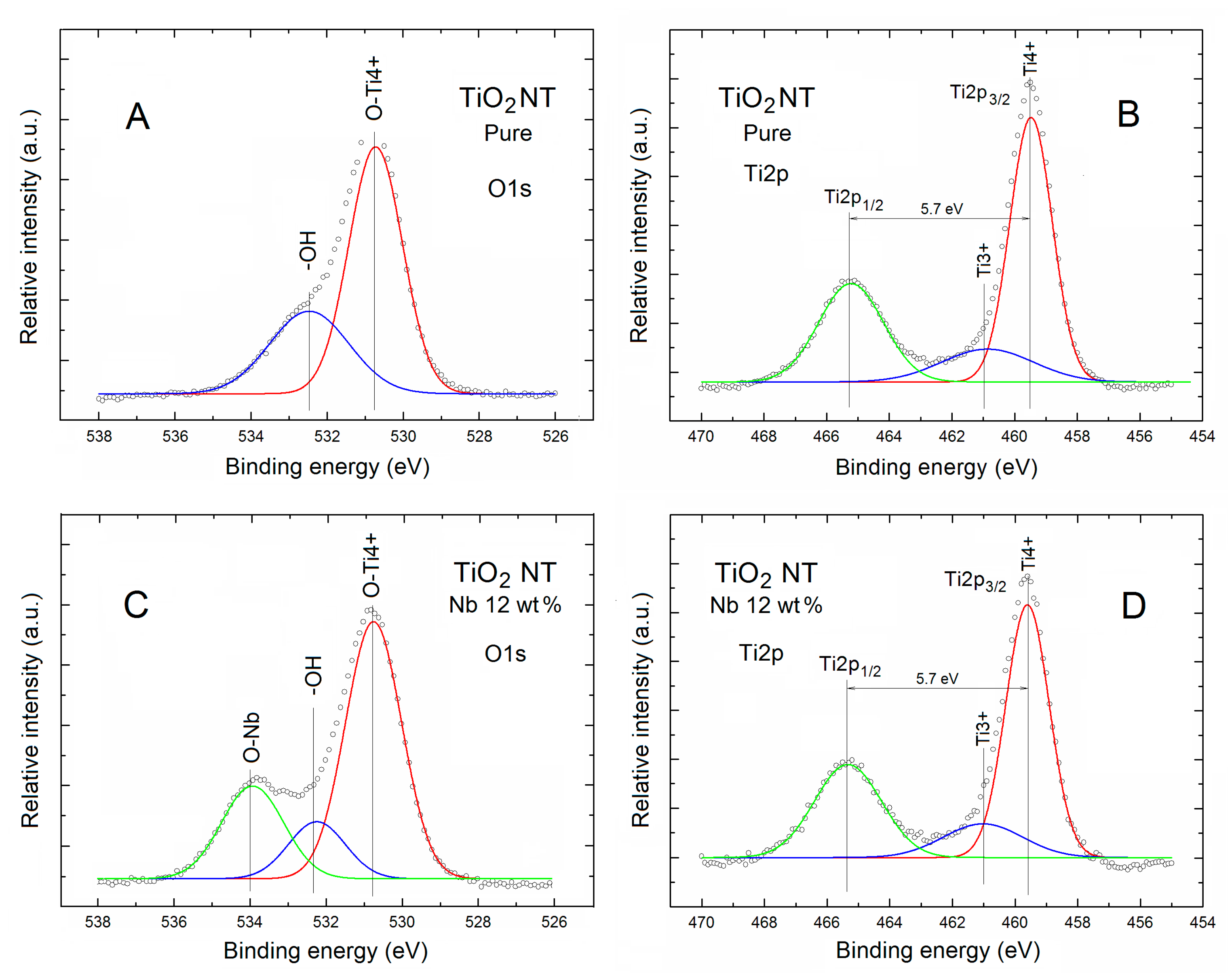
Figure 2 shows the XPS O1s and double Ti2p spectral lines of pure and Nb-doped TNT after deconvolution using Gauss fitting procedure.
As has been mentioned earlier, for Nb-doped TNT higher nonstoichiometry of the main matrix TiO2 was observed with respect to the pure ones. It means that one can expect different O surface bonding for both samples. This has been confirmed in our detailed analysis of the XPS O1s spectral lines after Gauss deconvolution procedure, as shown in Figure 2 (left column).
For the pure TNT, only two O components were recognized, as shown in Figure 2A.
The first one (as red), higher in intensity, is located at about 530.5 eV, can be attributed to the lattice oxygen bonded to O-Ti4+ bonding at the surface of pure TNT, which was in a good agreement, among others, with the TNT array by Mahajan et al. [28], as well as with the TiO2 thin films by Mohanta et al. [29].
The second one (as blue), lower in intensity, is located at about 532.5 eV, can be attributed to the different forms of surface hydroxyl bonding like –OH that can be present at the pure TNT surface after air exposure, which was observed for the highly porous TiO2 thin films with nanocrystalline framework by Kondalkar et al. [30].
However, this contribution can also reflects the presence of oxygen from carboxyl and alcohol groups adsorbed at the TiO2 surface that cannot be also excluded, as suggested by Gao et al. [31]. Moreover, it cannot also be excluded that this component is related partially to the contribution of SiO2 covering the Si substrate ,as well hydroxyl groups adsorbed at the SiO2 surface (having similar binding energies [32]), because at least TNT were deposited on such SiO2/Si substrate.
An evidently different shape of XPS O1s spectral line was observed for the Nb-doped TNT, as shown in Figure 2C. Apart from the two components observed above, in this case an evident component appeared (as green) at binding energy of about 534 eV, which can be attributed to the Nb oxides in form of diametric niobium oxide O–Nb=O, as observed recently by Chennakesavulu et al. [32] at the surface of an Nb2O5/ZnO catalyst.
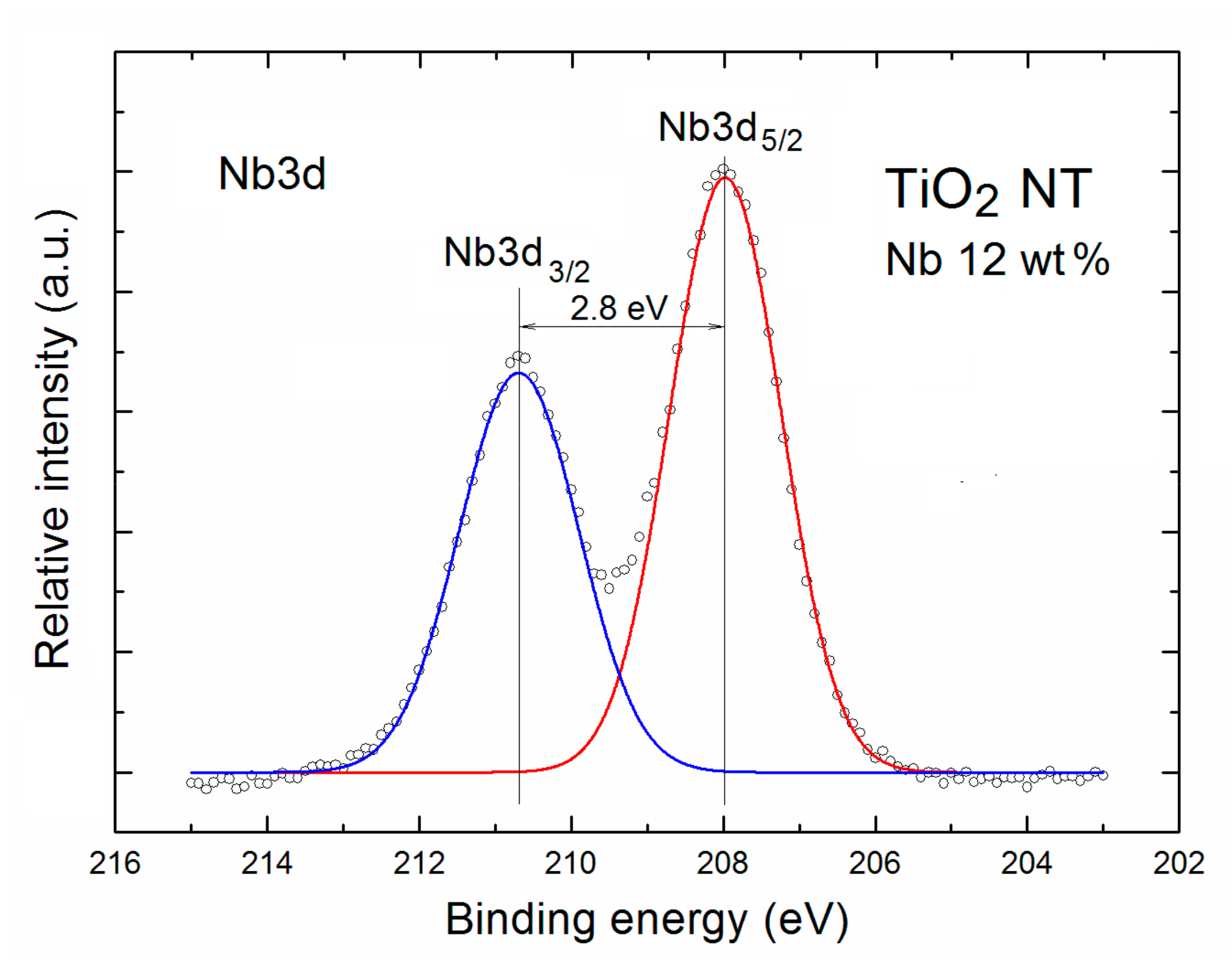
This last information is in a good correlation with the shape of spin orbit doublet XPS Nb3d spectral line of Nb-doped TNT after the Gauss deconvolution procedure shown in Figure 3, which will be discussed in more details below.
In relation to analysis of components of XPS O1s spectral lines shown in Figure 2A,C at the next step a detailed analysis of the XPS Ti2p spectral line of the pure and Nb-doped TNT was performed.
What is shown in Figure 2B,D for both TNT samples the XPS Ti2p core-level spectral lines contain the spin orbit doublet at binding energy of 459.6 eV (Ti2p3/2) (as red) and at a binding energy about 465.3 eV (Ti2p1/2) (as green) with the separation binding energy of 5.7 eV and intensity ratio of 0.5, which was in a good agreement with data obtained recently by Xu et al. [24].
In order to verify additionally an existence of any potential Ti ions of different valences in both TNT samples the Gauss deconvolution fitting procedure was applied for the higher Ti2p3/2 spectral lines, and for both samples two components were observed, as shown in Figure 2B,D.
A first one located at 459.5 eV can be assigned to the main Ti4+ bonding in TiO2, whereas a second one located at about 460.9 eV can be attributed to the Ti3+ bonding, probably related to the unsaturated Ti3+ adjacent to oxygen vacancy, as also observed for the titanium/silica nanostructured system exposed to molecular oxygen by Martinez-Mendez et al. [33], for the Nb-doped TiO2 thin films by Tucker et al. [34], and for the self-aligned TNT arrays by Anthony et al. [35]. It should be noted at this moment that the related intensity (area) of respective [Ti3+]/[Ti4+] components was equal to 0.27.
What is important the binding energy values of the above-described Ti components observed in our studies are in a good agreement with the values reported for various forms of TiO2 in the NIST database [36]. It should be additionally noted at this moment that, in our present study of the pure TNT, the existence of Ti2+ state of was not identified.
The only small difference for the Nb-doped TNT was in the related intensity (area) of the respective components [Ti3+]/[Ti4+] because it slightly decreased to the value of 0.23. This means that it differs only by about 15%, whereas the difference between the partial concentration of Ti in both samples was at the level of 35%; this was also summarized in Table 1.
As was mentioned above for the Nb-doped TNT, the additional evident component appeared in the XPS O1s spectral line with a binding energy of about 534 eV, which has been attributed to the Nb oxides in the form of diametric niobium oxide O–Nb=O.
This information was in a good correlation with the shape of respective XPS Nb3d spectral line after the Gauss deconvolution procedure shown in Figure 3.
It contains the spin orbit doublet at a binding energy of 207.9 eV (Nb3d5/2) and at a binding energy about 210.7 eV (Nb3d3/2), respectively, with the separation binding energy of 2.8 eV, and the intensity ratio of 0.72.
The obtained binding energies of both Nb components were in a good agreement with the data recently published, among other, Mohanta et al. [29] and by Tucker et al. [34], as well as with data available in the NIST database [36]. The Nb3d5/2 components observed in our studies confirm the existence of the pure niobium oxides Nb2O5 [37] at the surface of Nb-doped TNT.
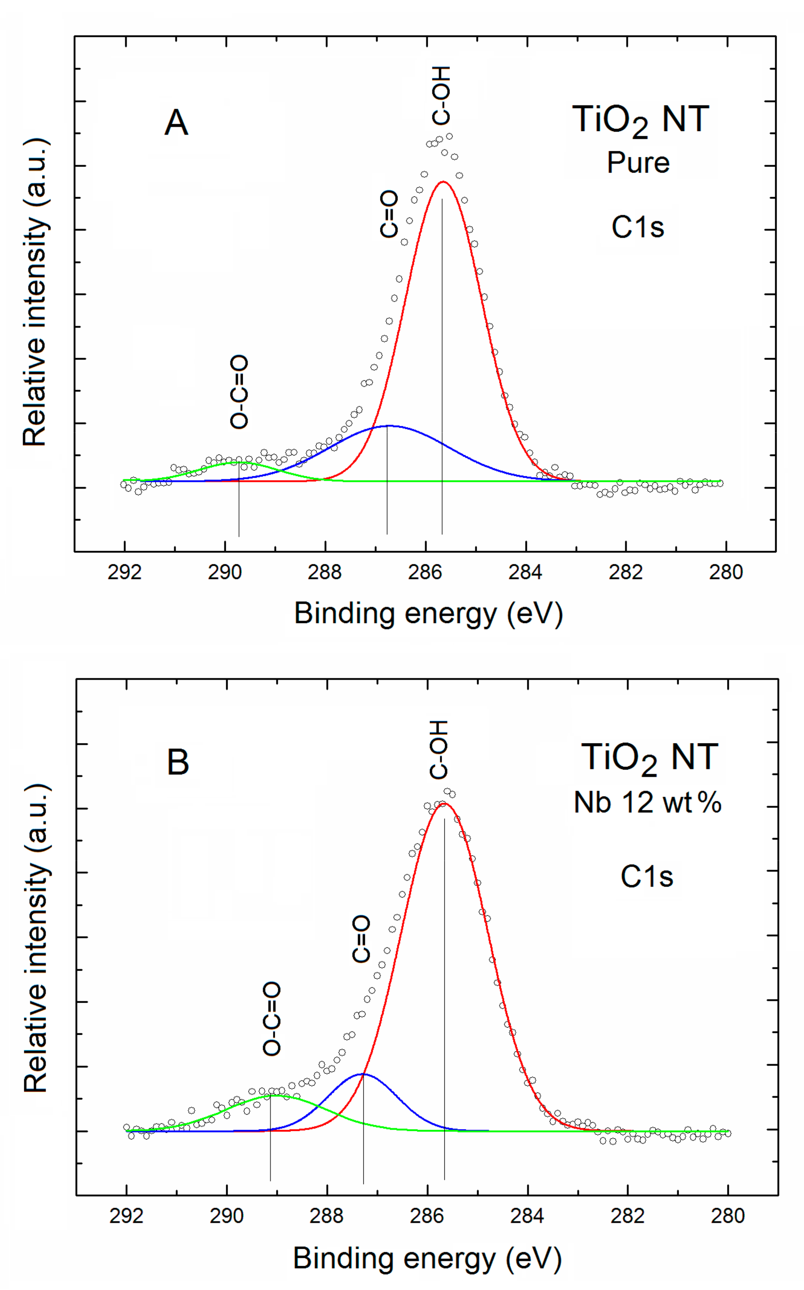
At this point it should be underlined that the potential existence of the hydroxyl groups at the surface of TNT after air exposure is in a good correlation with the fact that their existence was confirmed by the specific component in the XPS C1s spectral lines after the Gauss deconvolution procedure, as shown in Figure 4.
As shown in Figure 4A,B for both TNT samples XPS C1s spectral lines contain three evident components.
A first one, evidently highest in intensity, is located at binding energy about 286 eV, and can be attributed to the C bonding with water vapor components like C–OH at the surface of TNT after air exposure since this type of bonding are commonly observed at the oxide surfaces.
In turn, a second one, of evidently lower intensity (only 30% of the first one), located at the binding energy about 287 eV, can be attributed to the C bonding with oxygen surface contamination like C=O also commonly observed at oxide surfaces after air exposure.
Finally, a third one, of evidently lowest intensity (only 18% of the first one), located at the binding energy about 288 eV, can be attributed to the another C bonding with oxygen surface contamination like O–C=O, also commonly observed at oxide surfaces after air exposure. What is important is that the similar types of C surface bonding were also observed for the anodic oxide formed on Ti–Nb–Sn alloy by Ohtsu et al. [38], at the surface of Nb-doped TiO2 thin films prepared by the sol-gel method by Atashbar et al. [39], and at the surface of anatase TiO2 nanoparticles by Karthick et al. [40].
As mentioned above, also for the Nb-doped TNT three evident C components were observed with only small shift in binding energy of the second and third components. Moreover, an evident variation of the intensity of second and third components was observed, that is, they exhibit only 14% and 12% of the first one, what means that the contribution of C=O surface bonding was evidently smaller.
For the additional deeper analysis of C issue, we had in mind to consider the ion sputtering to remove the topmost layer of our TNT samples. However, this procedure looks rather doubtful because of two reasons:
Firstly, during the sputtering the ion Ar+ beam is commonly used of diameter of ~mm and focused perpendicularly (or at the specific angle to avoid its implantation) at the sample surface. However, in our studies we used the TiO2 NTs, which were aligned almost perpendicularly to the Si substrate (as seen in Figure 5). In such a case, what is absolutely crucial is that the ion beam not penetrates across the TiO2 NTs, but along their length. Thus, at such configuration, we are not able to obtain any reliable in depth information concerning the C contaminations across the TiO2 NTs of cylindrical surface of diameter ~50 nm, having additionally in mind that the diameter of X-ray beam using in XPS studies is ~3 mm.
Secondly, in the relation to our long-term experience in ion depth profiling studies, we had also in mind that during the ion sputtering the additional undesired effect commonly appears related to the fact that the ion Ar+ beam commonly generates the so-called “deep craters”, containing at their side surface the atoms not directly related to the atoms located primarily at the specific depth inside the subsurface of sample under investigation. This type of undesired effect was observed in our recent study of the ion depth profiling of SnO2 nanolayers deposited by the Laser-enhanced Chemical Vapor Deposition (L-CVD) method [41].
In addition to all the XPS information above on local surface chemistry of pure and Nb-doped TNT, at this point a contribution of Si substrate covered by SiO2 in the survey spectra of both samples confirmed by the existence of an evident XPS Si2p spectral lines visible in Figure 1 will be precisely analyzed below.
For the pure TNT the level of signal-to-noise ratio (S/N) for XPS Si2p spectral line was close to 5, whereas for the Nb-doped TNT it was almost two times larger.
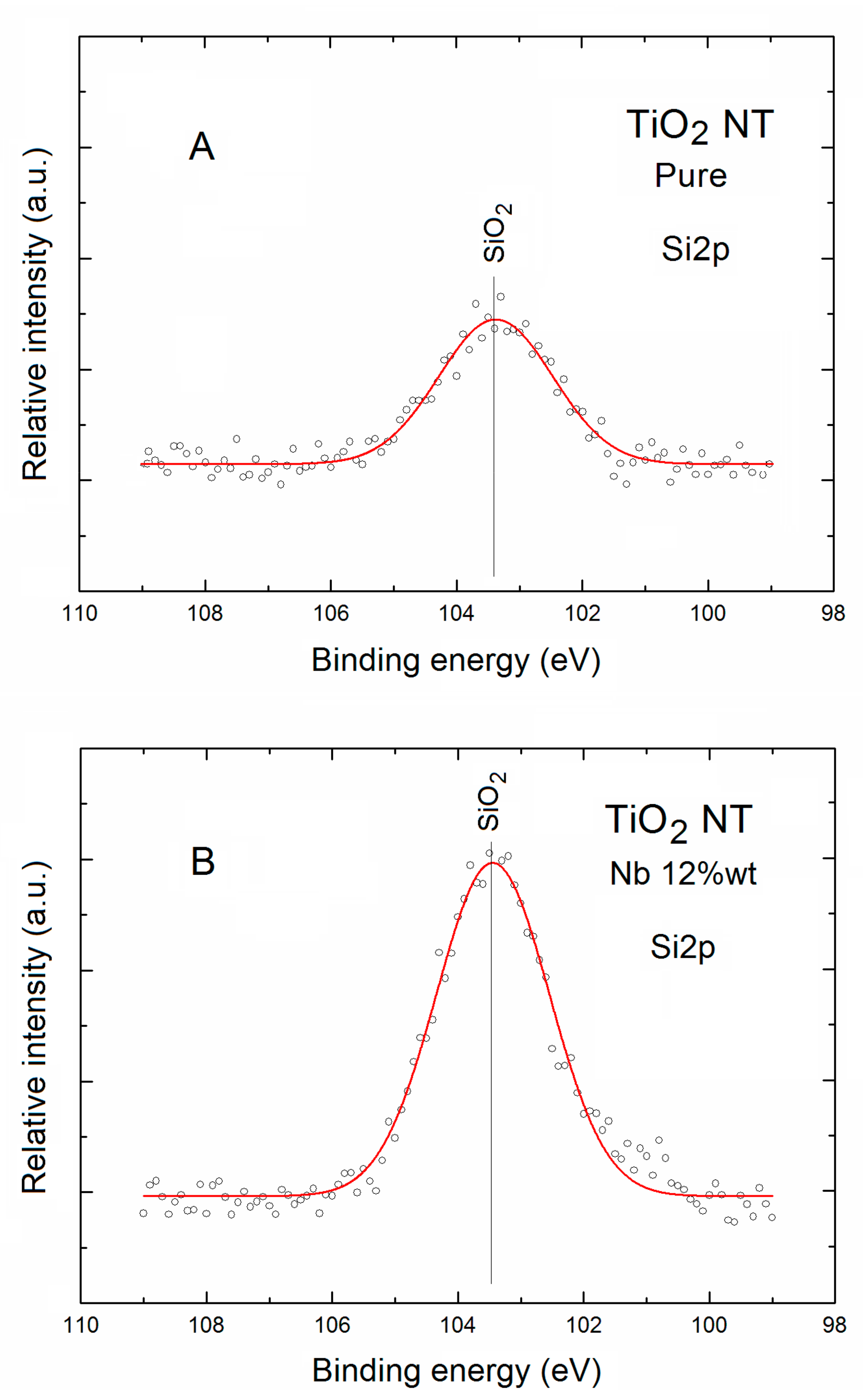
In order to check (verify) any surface Si ions of different valences related to the various SiO2 substrate surface bonding, the deconvolution fitting procedure was also applied for the XPS Si2p spectral lines for both TNT samples, what was shown in Figure 5.
As can be seen in Figure 5A,B the XPS Si2p spectral lines for both TNT samples contain only one evident component.
The binding energy location of this component was about 103.5 eV, which can be assigned to the SiO2 surface bonding at the Si substrate. The only difference in the deconvoluted XPS Si2p spectra is related in their evidently various relative intensity, clearly visible in Figure 5A,B.
What is important the binding energy of the main SiO2 surface bonding at the Si substrate observed in our studies was in a good agreement with the value reported recently by Alam et al. [42], as well as with data available in the NIST database [36]. It should be additionally noted at this moment that, in our present study, for both TNT samples the existence of another states (valences) of Si surface bonding were not identified.
An appearance of the contribution from SiO2 substrate in our XPS spectra of both TNT samples can be interpreted on the base of specific surface morphology of both TNT samples deposited on the SiO2/Si substrate.
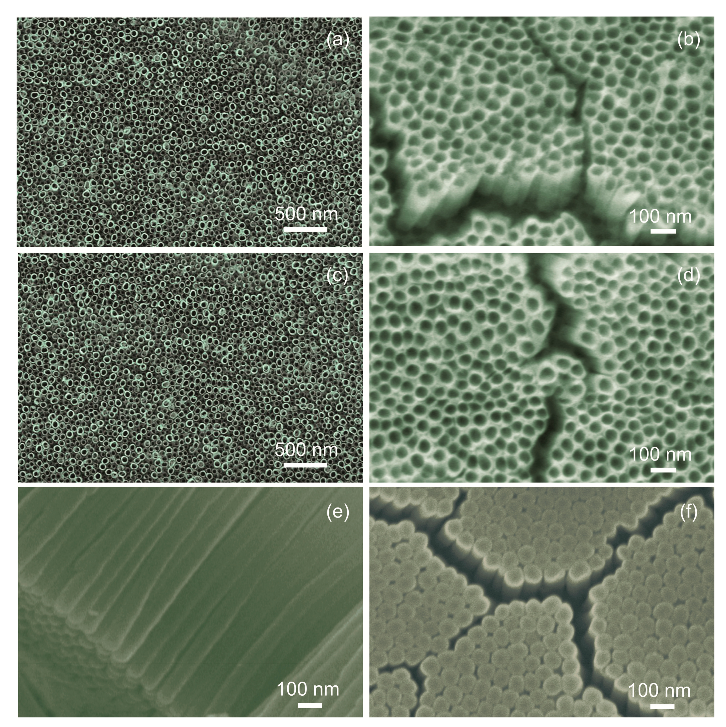
We have obtained pure and doped TiO2 nanotubes with the similar diameters and length by the variation of anodization parameters. Figure 6 shows the SEM micrographs of the obtained pure and 12 wt % doped TNT. The average internal and external diameters of pure and doped nanotubes are 45 and 75 nm, respectively. The length is about 1.7 µm. The relative standard deviation (RSD) is ~15%. The average diameters were determined from the SEM images taken from different locations of the sample and by measuring 50 tubes. The surface morphology (Figure 6a–d), cross-sectional (Figure 6e) and bottom-view (Figure 6f) of the structures show well-aligned and individual nanotubes were grown on Si/SiO2 substrates.
However, what is also clearly visible in Figure 6, between the specific slops containing several nanotubes an evident free spaces are observed, which probably originates from the fact that contribution from SiO2 covering the Si substrate, as well hydroxyl groups, adsorbed at the SiO2 surface (having a similar binding energies [32]) in the respective XPS O1s and XPS Si2p lines was observed, as discussed above.
3. Materials and Methods
Pure (TNT) and highly Nb-doped (12 wt %) TiO2 nanotubes (Nb-TNT) have been obtained at the Department of Information Engineering, Brescia University, Italy, using a two-step process.
Within the first step Ti and Ti–Nb films were deposited on Si substrates covered by SiO2 by means of RF (13.56 MHz) magnetron sputtering using the targets of Ti and Ti with the holes filled by Nb insets. Within the second step the room-temperature anodization process of Ti and Ti–Nb films was performed using a two-electrode system working at constant voltage mode (potentiostatic mode) using an electrolyte a mixture of 0.3–1 wt % NH4F and 0.5–2 mol/L H2O in glycerol. We have obtained pure nanotubes in 0.5 wt % NH4F and 0.5 mol/L H2O containing glycerol. The anodization voltage and time were 120 V and 45 min. Nb-TNT were obtained in 1 wt % NH4F and 0.5 mol/L H2O containing glycerol. The anodization voltage and time for the preparation of Nb-TNT were 120 V and 35 min.
After anodization the samples were washed in distilled water and dried at room temperature. In order to transfer the deposited amorphous phase to the anatase phase the samples were annealed at 400 °C for 5 h in air. Other experimental details on the preparation of Ti and Ti/Nb films and their anodization one can find in [20,21,22].
The surface chemistry, including contaminations, of the prepared pure and Nb-doped TiO2 nanotubes was controlled by XPS method. These experiments were performed at Institute of Electronics, Silesian University of Technology, Gliwice, Poland, using a commercial XPS spectrometer (SPECS, Berlin, Germany) equipped, among others, with the X-ray lamp (XR-50) and a concentric hemispherical analyzer (PHOIBOS-100). The basic working pressure was at the level ~10−9 hPa. All the reported binding energies (BE) data have been calibrated to Au4f peak at 84.0 eV. Other experimental details have been described elsewhere [23,41,43].
In turn, the morphological characterization of the above mentioned TiO2 NT was carried out at the Department of Information Engineering, Brescia University, Italy, by the SEM method using a LEO 1525 microscope (LEO Electron Microscopy Inc., One Zeiss Drive, Thornwood, NY, USA) equipped with field emission gun.
4. Conclusions
The surface chemistry of pure and 12 wt % Nb-doped TNTs deposited on Si substrates covered by SiO2 were studied by means of the XPS method. The obtained results were in a good correlation with the samples’ morphological characteristics.
For the pure TNTs the relative concentration of specific elements O, Ti and C, with respect to all the surface atoms, was equal to 0.46, 018 and 0.36, respectively. For the highly Nb-doped (12 % wt) TNT a slightly different surface chemistry was observed since the relative concentrations of specific elements O and Ti, and with respect to all the surface atoms, were slightly lower, 0.42 and 0.12. This is related to the fact that Nb atoms appeared at the surface having the relative concentration with respect to all the surface atoms at the level of 0.09.
An evident free space was observed between the specific slops containing several TNT by means of SEM analysis, which was additionally confirmed by the contribution from the SiO2/Si substrate containing in the respective XPS O1s and XPS Si2p lines as well.
The obtained results allowed us a new insight on the potential origin of aging effect for TiO2 nanotubes in atmosphere being the undesired limitation for their potential application as the chemical sensors.
Acknowledgments
This work was supported by the Ministry of Science and Higher Education funding for statutory activities of the Institute of Electronics, Silesian University of Technology, Gliwice, Poland and the European EuNetAir Project, COST Action TD1105 and partially financed by research grant of National Science Centre, Poland—OPUS 11, no 2016/21/B/ST7/02244. The work has also been supported by the projects “New approaches and methodologies for bioremediation of water contaminated by chlorinated aliphatic solvents (SUSBIOREM)” (funded by the National Research Council (CNR) and Lombardia Region) and “MSP: Multi Sensor Platform for Smart Building Management” (grant agreement No 611887, funded by the European Commission through its 7th Framework Programme).
Author Contributions
M.K. involved in carrying out the XPS experiments, analyzing the experimental data and drafting the manuscript; V.G. involved in the preparation of samples and SEM experiments with data analysis; E.C. and J.S. conceived of the study. All authors read and approved the final version of the manuscript.
Conflicts of Interest
The authors declare no conflict of interest.
References
- Jiu, J.; Isoda, S.; Wang, F.; Adachi, M. Dye-sensitized solar cells based on a single-crystalline TiO2 nanorod. J. Phys. Chem. B 2006, 110, 2087–2092. [Google Scholar] [CrossRef] [PubMed]
- Varghese, K.; Paulose, M.; Grimes, C.A. Long vertically aligned titania nanotubes on transparent conducting oxide for highly efficient solar cells. Nat. Nanotechnol. 2009, 4, 592–597. [Google Scholar] [CrossRef] [PubMed]
- Galstyan, V.; Vomiero, A.; Concina, I.; Braga, A.; Brisotto, M.; Bontempi, E.; Faglia, G.; Sberveglieri, G. Vertically aligned TiO2 nanotubes on plastic substrates for flexible solar cells. Small 2011, 7, 2437–2442. [Google Scholar] [CrossRef] [PubMed]
- Yuxiang, Y.; Dongsheng, X. Single-crystalline TiO2 nanorods: Highly active and easily recycled photocatalysts. Appl. Catal. B Environ. 2007, 73, 166–171. [Google Scholar]
- Kang, A.-Z.; Xu, Z.; Song, Y.; Mu, J. Photocatalytic activity of high aspect ratio TiO2 nanorods. J. Dispers. Sci. Technol. 2006, 27, 857–859. [Google Scholar] [CrossRef]
- Akbar, S.A.; Younkman, L.B. Sensing mechanism of a carbon monoxide sensor based on anatase titania. J. Electrochem. Soc. 1997, 144, 1750–1753. [Google Scholar] [CrossRef]
- Harris, L.A. A titanium-dioxide hydrogen detector. J. Electrochem. Soc. 1980, 127, 2657–2662. [Google Scholar] [CrossRef]
- Satake, K.; Katayama, A.; Ohkoshi, H.; Nakahara, T.; Takeuchi, T. Titania NOx sensors for exhaust monitoring. Sens. Actuators B Chem. 1994, 20, 111–117. [Google Scholar] [CrossRef]
- Comini, E.; Sberveglieri, G.; Ferroni, M.; Guidi, V.; Martinelli, G. Response to ethanol of thin films based on Mo and Ti oxides deposited by sputtering. Sens. Actuators B Chem. 2003, 93, 409–415. [Google Scholar] [CrossRef]
- Galstyan, V.; Comini, E.; Baratto, C.; Ponzoni, A.; Ferroni, M.; Poli, N.; Faglia, G.; Bontempi, E.; Brisotto, M.; Sberveglieri, G. Large surface area biphase titania for chemical sensing. Sens. Actuators B Chem. 2015, 209, 1091–1096. [Google Scholar] [CrossRef]
- Du, G.H.; Chen, Q.; Che, R.C.; Yuan, Z.Y.; Peng, L.M. Preparation, structure analysis of titanium oxide nanotubes. Appl. Phys. Lett. 2001, 79, 3702–3704. [Google Scholar] [CrossRef]
- Alessandri, I.; Comini, E.; Bontempi, E.; Faglia, G.; Depero, L.E.; Sberveglieri, G. Cr-inserted TiO2 thin films for chemical gas sensors. Sens. Actuators B Chem. 2007, 128, 312–319. [Google Scholar] [CrossRef]
- Zhang, X.X.; Zhang, J.B.; Jia, Y.C.; Xiao, P.; Tang, J. TiO2 nanotube array sensor for detecting the SF6 decomposition product SO2. Sensors 2012, 12, 3302–3313. [Google Scholar] [CrossRef] [PubMed]
- Körner, W.; Elsässer, C. Density functional theory study of dopants in polycrystalline TiO2. Phys. Rev. B 2011, 83, 205315. [Google Scholar] [CrossRef]
- Sotter, E.; Vilanova, X.; Llobet, E.; Stankova, M.; Correig, X. Niobium-doped titania nanopowders for gas sensor applications. J. Optoel. Adv. Mater. 2005, 7, 1395–1398. [Google Scholar]
- Edelman, F.; Hahn, H.; Seifried, S.; Alof, C.; Hoche, H.; Balogh, A.; Werner, P.; Zakrzewska, K.; Radecka, M.; Pasierb, P.; et al. Structural evolution of SnO2-TiO2 nanocrystalline films for gas sensors. Mater. Sci. Eng. B 2000, 69–70, 386–391. [Google Scholar] [CrossRef]
- Lee, H.; Leu, I.C.; Hsu, M.C.; Chung, Y.W.; Hon, M.H. Fabrication of aligned TiO2 one-dimensional nanostructured arrays using a one-step templating solution approach. J. Phys. Chem. B 2005, 109, 13056–13059. [Google Scholar] [CrossRef] [PubMed]
- Hoyer, P. Formation of titanium dioxide nanotube array. Langmuir 1996, 12, 1411–1413. [Google Scholar] [CrossRef]
- Galstyan, V.; Comini, E.; Faglia, G.; Sberveglieri, G. TiO2 Nanotubes: Recent advances in synthesis and gas sensing properties. Sensors 2013, 13, 14813–14838. [Google Scholar] [CrossRef] [PubMed]
- Galstyan, V.; Comini, E.; Vomiero, A.; Ponzoni, A.; Concina, I.; Brisotto, M.; Bontempi, E.; Faglia, G.; Sberveglieri, G. Fabrication of pure and Nb-TiO2 nanotubes and their functional properties. J. Alloys Comp. 2012, 536, S488–S490. [Google Scholar] [CrossRef]
- Galstyan, V.; Comini, E.; Faglia, G.; Vomiero, A.; Borgese, L.; Bontempi, E.; Sberveglieri, G. Fabrication and investigation of gas sensing properties of Nb-doped TiO2 nanotubular arrays. Nanotechnology 2012, 23, 235706. [Google Scholar] [CrossRef] [PubMed]
- Comini, E.; Galstyan, V.; Faglia, G.; Bontempi, E.; Sberveglieri, G. Highly conductive titanium oxide nanotubes chemical sensors. Microporous Mesoporous Mater. 2015, 208, 165–170. [Google Scholar] [CrossRef]
- Kwoka, M.; Ottaviano, L.; Szuber, J. Photoemission studies of the surface electronic properties of L-CVD SnO2 ultra thin films. Appl. Surf. Sci. 2012, 258, 8425–8429. [Google Scholar] [CrossRef]
- Xu, Z.; Li, Q.; Gao, S.; Shang, J. Synthesis and characterization of niobium-doped TiO2 nanotube arrays by anodization of Ti-20Nb alloys. J. Mater. Sci. Technol. 2012, 28, 865–870. [Google Scholar] [CrossRef]
- Moulder, J.F.; Stickle, W.F.; Sool, P.E.; Bomben, K.D. Handbook of X-ray Photoelectron Spectroscopy; Perkin-Elmer: Eden Prairie, MN, USA, 1992; ISBN 0962702625. [Google Scholar]
- Watts, J.F.; Wolstenholme, J. An Introduction to Surface Analysis by XPS and AES; John Wiley & Sons: Chichester, UK, 2003; ISBN 978-0-470-84713-8. [Google Scholar]
- Surface Analysis—The Principal Techniques, 2nd ed; Vickerman, J.C.; Gilmore, I.S. (Eds.) John Wiley & Sons: Chichester, UK, 2009; ISBN 978-0-470-01763-0. [Google Scholar]
- Mahajan, V.K.; Misra, M.; Raja, K.S.; Mohapatra, S.K. Self-organized TiO2 nanotubular arrays for photoelectrochemical hydrogen generation: Effect of crystallization and defect structures. J. Phys. D Appl. Phys. 2008, 41, 125307–125315. [Google Scholar] [CrossRef]
- Mohanta, R.R.; Medicherla, V.R.R.; Mohanta, K.L.; Nayak, N.C.; Majumder, S.; Solanki, V.; Varma, S.; Bapna, K.; Phase, D.M.; Sathe, V. Ion beam induced chemical and morphological changes in TiO2 films deposited on Si(111) surface by pulsed laser deposition. Appl. Surf. Sci. 2015, 325, 185–191. [Google Scholar] [CrossRef]
- Kondalkar, V.V.; Mali, S.S.; Pawar, N.B.; Mane, R.M.; Choudhury, S.; Hong, C.K.; Patil, P.S.; Patil, S.R.; Bhosalea, P.N.; Kim, J.H. Microwave-assisted rapid synthesis of highly porous TiO2 thin films with nanocrystalline framework for efficient photoelectrochemical conversion. Electrochim. Acta 2014, 143, 89–97. [Google Scholar] [CrossRef]
- Gao, Y.-F.; Masuda, Y.; Koumoto, K. Light-Excited superhydrophilicity of amorphous TiO2 thin films deposited in an aqueous peroxotitanate solution. Langmuir 2004, 20, 3188–3194. [Google Scholar] [CrossRef] [PubMed]
- Chennakesavulu, K.; Reddy, G.R.; Prasath, S.S.; Supriya, S.; Sivanesan, S. Visible light driven photocatalytic degradation of the reactive red-198, methylene blue and 3-chlorophenol by Nb2O5@ZnO: Synthesis and characterization. Adv. Mater. Lett. 2015, 6, 518–526. [Google Scholar] [CrossRef]
- Martinez-Mendez, S.; Henriquez, Y.; Dominguez, O.; D’Ornelas, L.; Krentzien, H. Catalytic properties of silica supported titanium, vanadium and niobium oxide nanoparticles towards the oxidation of saturated and unsaturated hydrocarbons. J. Mol. Catal. A Chem. 2006, 252, 226–234. [Google Scholar] [CrossRef]
- Tucker, R.T.; Beckers, N.A.; Fleischauer, M.D.; Brett, M.J. Electron beam deposited Nb-doped TiO2 toward nanostructured transparent conductive thin films. Thin Solid Films 2012, 525, 28–34. [Google Scholar] [CrossRef]
- Antony, R.P.; Mathews, T.; Dash, S.; Tyagi, A.K.; Raj, B. X-ray photoelectron spectroscopic studies of anodically synthesized self aligned TiO2 nanotube arrays and the effect of electrochemical parameters on tube morphology. Mater. Chem. Phys. 2012, 132, 957–966. [Google Scholar] [CrossRef]
- Wagner, C.D.; Naumkin, A.V.; Kraut-Vass, A.; Allison, J.W.; Powell, C.J.; Rumble, J.R.J. NIST X-ray Photoelectron Spectroscopy Database; NIST NSRDS: Gaithersburg, MD, USA, 2003. [Google Scholar]
- Cottineau, T.; Bealu, N.; Gross, P.-A.; Pronkin, S.N.; Keller, N.; Savinova, E.R.; Keller, V. One step synthesis of niobium doped titania nanotube arrays to form (N, Nb) co-doped TiO2 with high visible light hotoelectrochemical activity. J. Mater. Chem. A 2013, 1, 2151–2160. [Google Scholar] [CrossRef]
- Ohtsu, N.; Masahashi, N.; Mizukoshi, Y. Angle resolved XPS studies on an anodic oxide formed on Ti–Nb–Sn alloy and the photo-induced change in carbon contaminants adsorbed on its surface. Appl. Surf. Sci. 2012, 258, 6052–6055. [Google Scholar] [CrossRef]
- Atashbar, M.Z.; Sun, H.T.; Gong, B.; Wlodarski, W.; Lamb, R. XPS study of Nb-doped oxygen sensing TiO2 thin films prepared by sol-gel method. Thin Solid Films 1998, 326, 238–244. [Google Scholar] [CrossRef]
- Karthick, S.N.; Prabakar, K.; Subramania, A.; Hong, J.-T.; Jang, J.-J.; Kim, H.-J. Formation of anatase TiO2 nanoparticles by simple polymer gel technique and their properties. Powder Technol. 2011, 205, 36–41. [Google Scholar] [CrossRef]
- Kwoka, M.; Ottaviano, L.; Passacantando, M.; Santucci, S.; Szuber, J. XPS depth profiling studies of L-CVD SnO2 thin films. Appl. Surf. Sci. 2006, 252, 7730–7733. [Google Scholar] [CrossRef]
- Alam, A.U.; Howlader, M.M.R.; Deen, M.J. Oxygen plasma and humidity dependent surface analysis of silicon, silicon dioxide and glass for direct wafer bonding. ECS J. Solid State Sci. Technol. 2013, 2, P515–P523. [Google Scholar] [CrossRef]
- Sitarz, M.; Kwoka, M.; Comini, E.; Zappa, D.; Szuber, J. Surface chemistry of the SnO2 nanowires on Ag catalyst-covered Si substrate studied by XPS and TDS methods. Nanoscale Res. Lett. 2014, 9, 43. [Google Scholar] [CrossRef] [PubMed]
Figure 1.
X-ray photoelectron spectroscopy (XPS) survey spectra of pure and Nb-doped TiO2 nanotubes.
Figure 1.
X-ray photoelectron spectroscopy (XPS) survey spectra of pure and Nb-doped TiO2 nanotubes.
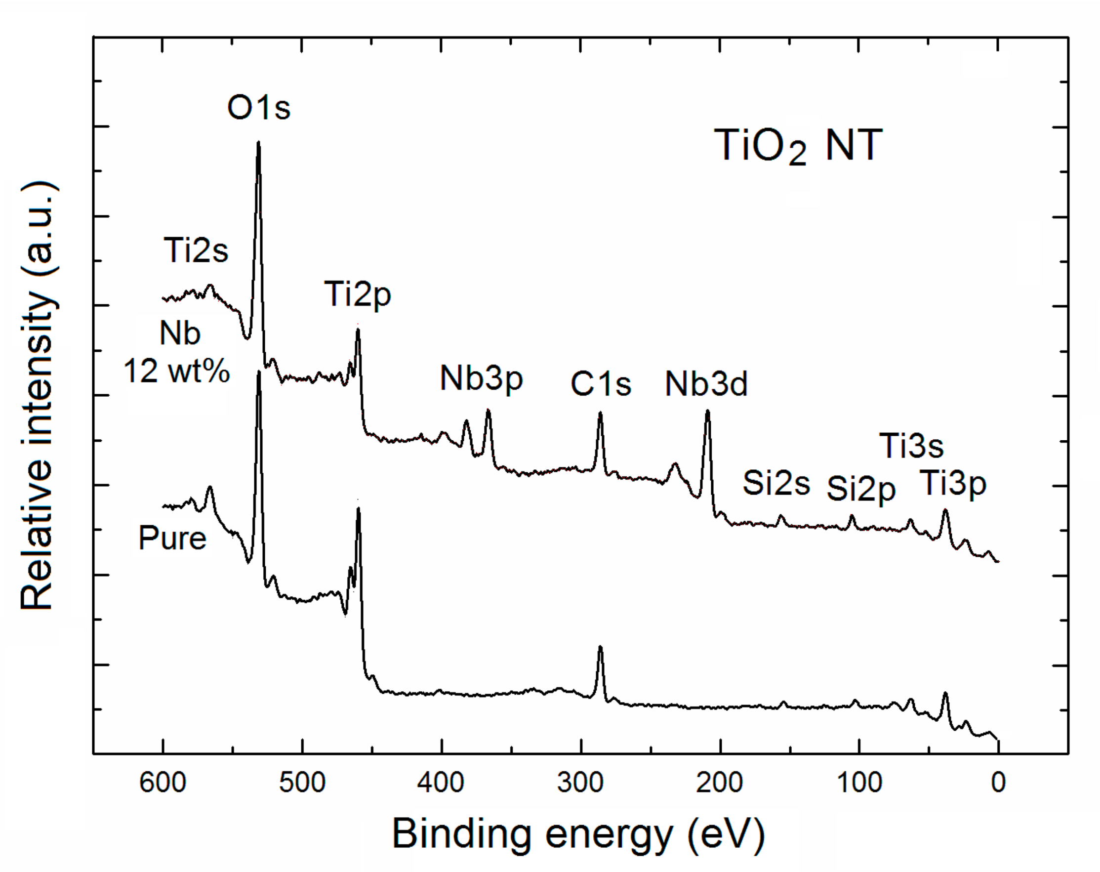
Figure 2.
XPS O1s and double Ti2p spectral lines of pure (A,B) and Nb-doped (C,D) TNT, respectively, after Gauss deconvolution. The circles correspond to the experimental curves after linear smoothing, whereas the color lines correspond to the respective deconvoluted components.
Figure 2.
XPS O1s and double Ti2p spectral lines of pure (A,B) and Nb-doped (C,D) TNT, respectively, after Gauss deconvolution. The circles correspond to the experimental curves after linear smoothing, whereas the color lines correspond to the respective deconvoluted components.

Figure 3.
XPS Nb3d spectral line of Nb-doped TNT after Gauss deconvolution. The circles correspond to the experimental curves after linear smoothing, whereas the color lines correspond to the respective spin orbit doublet.
Figure 3.
XPS Nb3d spectral line of Nb-doped TNT after Gauss deconvolution. The circles correspond to the experimental curves after linear smoothing, whereas the color lines correspond to the respective spin orbit doublet.

Figure 4.
XPS C1s spectral lines of (A) pure and (B) Nb-doped TNT after the Gauss deconvolution. The circles correspond to the experimental curves after linear smoothing, whereas the color lines correspond to the respective deconvoluted components.
Figure 4.
XPS C1s spectral lines of (A) pure and (B) Nb-doped TNT after the Gauss deconvolution. The circles correspond to the experimental curves after linear smoothing, whereas the color lines correspond to the respective deconvoluted components.

Figure 5.
XPS Si2p spectral lines of (A) pure and (B) Nb-doped TNT after Gauss deconvolution. The circles correspond to the experimental curves after linear smoothing, whereas the color lines correspond to the respective deconvoluted component.
Figure 5.
XPS Si2p spectral lines of (A) pure and (B) Nb-doped TNT after Gauss deconvolution. The circles correspond to the experimental curves after linear smoothing, whereas the color lines correspond to the respective deconvoluted component.

Figure 6.
Scanning electron microscopy (SEM) micrographs of the obtained tubular samples: (a) and (b) the surface morphology of pure TNT arrays with the different magnifications; (c,d) the surface morphology of 12 wt % Nb-doped TNTs with the different magnifications; (e) the cross-sectional view of 12 wt % Nb-doped TNTs, and; (f) the bottom-view of 12 wt % Nb-doped TiO2 tubular layer.


Table 1.
Relative concentration of specific elements (with respect to all the surface atoms), and the corresponding partial concentration (in %) of the basic elements of pure and highly doped (12 wt %) Nb-TiO2 nanotubes (TNT).
Table 1.
Relative concentration of specific elements (with respect to all the surface atoms), and the corresponding partial concentration (in %) of the basic elements of pure and highly doped (12 wt %) Nb-TiO2 nanotubes (TNT).
| TNT | Relative Concentration of Specific Elements with Respect to All the Surface Atoms | Partial Surface Concentration of Specific Elements (%) | ||||||
|---|---|---|---|---|---|---|---|---|
| O | Ti | Nb | C | O | Ti | Nb | C | |
| Pure | 0.46 | 0.18 | 0 | 0.36 | 46 | 18 | 0 | 36 |
| Nb-doped | 0.42 | 0.12 | 0.09 | 0.36 | 42 | 12 | 9 | 36 |
© 2017 by the authors. Licensee MDPI, Basel, Switzerland. This article is an open access article distributed under the terms and conditions of the Creative Commons Attribution (CC BY) license (http://creativecommons.org/licenses/by/4.0/).
Share and Cite
MDPI and ACS Style
Kwoka, M.; Galstyan, V.; Comini, E.; Szuber, J. Pure and Highly Nb-Doped Titanium Dioxide Nanotubular Arrays: Characterization of Local Surface Properties. Nanomaterials 2017, 7, 456. https://doi.org/10.3390/nano7120456
AMA Style
Kwoka M, Galstyan V, Comini E, Szuber J. Pure and Highly Nb-Doped Titanium Dioxide Nanotubular Arrays: Characterization of Local Surface Properties. Nanomaterials. 2017; 7(12):456. https://doi.org/10.3390/nano7120456
Chicago/Turabian StyleKwoka, Monika, Vardan Galstyan, Elisabetta Comini, and Jacek Szuber. 2017. "Pure and Highly Nb-Doped Titanium Dioxide Nanotubular Arrays: Characterization of Local Surface Properties" Nanomaterials 7, no. 12: 456. https://doi.org/10.3390/nano7120456
Note that from the first issue of 2016, this journal uses article numbers instead of page numbers. See further details here.