Next Article in Journal
I-V and C-V Characterization of a High-Responsivity Graphene/Silicon Photodiode with Embedded MOS Capacitor
Next Article in Special Issue
Colloidal Synthesis and Thermoelectric Properties of CuFeSe2 Nanocrystals
Previous Article in Journal
Oxygen Partial Pressure Impact on Characteristics of Indium Titanium Zinc Oxide Thin Film Transistor Fabricated via RF Sputtering
 
 
Correction published on 30 October 2017, see Nanomaterials 2017, 7(11), 357.
Article

Thermoelectric and Transport Properties of Delafossite CuCrO2:Mg Thin Films Prepared by RF Magnetron Sputtering

CIRIMAT, Université de Toulouse, CNRS, INPT, UPS, 118 route de Narbonne, F-31062 Toulouse CEDEX 9, France
*
Author to whom correspondence should be addressed.
Nanomaterials 2017, 7(7), 157; https://doi.org/10.3390/nano7070157
Submission received: 24 May 2017 / Revised: 20 June 2017 / Accepted: 21 June 2017 / Published: 27 June 2017
(This article belongs to the Special Issue Thermoelectric Nanomaterials)

Abstract

:
P-type Mg doped CuCrO2 thin films have been deposited on fused silica substrates by Radio-Frequency (RF) magnetron sputtering. The as-deposited CuCrO2:Mg thin films have been annealed at different temperatures (from 450 to 650 °C) under primary vacuum to obtain the delafossite phase. The annealed samples exhibit 3R delafossite structure. Electrical conductivity σ and Seebeck coefficient S of all annealed films have been measured from 40 to 220 °C. The optimized properties have been obtained for CuCrO2:Mg thin film annealed at 550 °C. At a measurement temperature of 40 °C, this sample exhibited the highest electrical conductivity of 0.60 S·cm−1 with a Seebeck coefficient of +329 µV·K−1. The calculated power factor (PF = σS²) was 6 µW·m−1·K−2 at 40 °C and due to the constant Seebeck coefficient and the increasing electrical conductivity with measurement temperature, it reached 38 µW·m−1·K−2 at 220 °C. Moreover, according to measurement of the Seebeck coefficient and electrical conductivity in temperature, we confirmed that CuCrO2:Mg exhibits hopping conduction and degenerates semiconductor behavior. Carrier concentration, Fermi level, and hole effective mass have been discussed.

1. Introduction

The thermoelectricity is a promising technique to overcome the issues in recovering waste heat to electricity without using moving parts. Thermoelectric (TE) effect is defined as the conversion of a temperature gradient directly into electricity and vice versa [1]. Thermoelectric generators have several advantages: they are particularly reliable, maintenance free, and durable with long operating life under extreme conditions [2].
The performance of the TE materials is described by the dimension less figure of merit ZT [1].
Z T = σ S 2 ( K e + K th ) × T
In these equations, σ and S are respectively the electrical conductivity and the Seebeck coefficient [3] at the given temperature T and Ke and Kth are respectively due to the electron transport and the lattice phonon at the given temperature T. The enhancement efforts of ZT is very challenging because of the σ, S, and Ke interdependence. Indeed, as the carrier density expands, the electrical conductivity increases and at the same time it reduces the Seebeck coefficient and increases the electronical thermal conductivity. To optimize TE materials, the Power Factor (PF = σS2) must be increased without increasing the global thermal conductivity. This can be done by improving the carrier concentration and the mobility and/or reducing the lattice thermal conductivity Kth by introducing scattering centers with point defects [4], interfaces [5], and nanostructuration [6].
The advantage of the thin films versus bulk materials is rarely guested with the PF. Only the Figure of Merit (ZT) can reveal it. In fact some macroscopic disorder can lead to a significant reduction of the thermal conductivity of thin films relative to that observed in bulk material [7,8,9]. As ZT takes into account the thermal conductivity, thin films could have better TE properties than the bulk thanks to their microstructures. Moreover, the low dimension system obtained in thin films could make a significant band structure modification that could impact the Seebeck coefficient.
Transition metal oxides (TMOs) are a captivating class of materials due to their wide ranging electronic, chemical, and mechanical properties. Furthermore, they are gaining increasing attention for their thermoelectric (TE) properties due to their high temperature stability, tunable electronic and phonon transport properties, and well-established synthesis techniques.
Delafossite type oxides CuIMIIIO2 with M = (Fe, Al, Ga, Cr…) due to their large range of properties and the abundance of their constituent elements in the nature, have been studied for several applications such as transparent p-type conducting oxides (TCO) [10,11,12,13,14,15,16,17], transparent electronic devices [18,19,20,21,22,23,24,25], dye-sensitized solar cells [26,27,28,29], and photoelectrodes [30] but also for outstanding catalysis [31] and photo-catalysis [31,32,33,34,35,36,37,38,39,40,41], antibacterial [42], luminescence [43,44,45], gas and temperature sensing [46,47,48,49], magnetic and electric [50,51,52,53,54], energy storage [55], oxygen storage [56], water reduction [57], thermoelectricity and superconductivity [58] properties. In the oxide family, the cation CuI is a monovalent metal and the cation MIII is a trivalent metal. Delafossite structure can be described as a stack of cation CuI layer and MO6 octahedron layer along c axis. Each cation CuI is linearly coordinated to two oxygens belonging to upper and lower MO6 octahedron. Even if Cu-based delafossite type oxides receive most of the attention for their optoelectronic properties as a p-type transparent semiconductor, they exhibit also interesting thermoelectric (TE) properties [59,60,61,62,63,64,65,66,67].
Among the Cu-based delafossites, CuCrO2 is currently of interest due to its attractive physical properties for the applications mentioned above [68,69,70,71,72,73,74,75,76,77,78]. Hayashi et al. [69] studied TE properties of CuCrO2 in bulk form with several dopants and reported that the Mg-doped samples showed a higher electrical conductivity leading to a higher power factor (PF = 2.36 × 10⁻⁴ W·m−1·K−2 at 820 °C) than the undoped bulk. In comparison with CuCrO2 and CuCrO2:Mg studies carried out on bulk materials [70,71,74,79,80], there is a lack of papers related to proper studies of the TE properties of CuCrO2:Mg thin films, as for instance, the determination of PF. Most of the time, Seebeck measurements presented in the bibliography are only used to characterize the fundamental physical properties (type of charge carriers, transport mechanism) [16,73,81,82,83,84,85] especially because it is difficult to determine the main charge carrier characteristics by conventional Hall measurements in this type of material. In particular, we have measured the Seebeck coefficient at room temperature for 100 nm thick films in order to determine the type of the main charge carrier in CuCrO2:Mg thin films optimized for TCO properties [16]. In the present article, the work is focused on the determination of electrical conductivities and TE properties (Seebeck coefficient and calculated power factor) in temperature ranging from 40 to 220 °C for one set of CuCrO2 films annealed at various temperatures, with a fixed thickness of 300 nm.

2. Materials and Methods

2.1. Preparation of Mg-Doped CuCrO2 (Target)

Polycrystalline CuCr0.97Mg0.03O2 powder was prepared by grinding and mixing the starting commercial oxides, Cu2O, Cr2O3, and MgO with appropriate proportions. The stoichiometric oxide mixture was annealed at 900 °C for 10 h in an ambient nitrogen atmosphere and cooled down to room temperature. After it was reground, the mixture was reheated for a further 10 h period. The purity of the phase was checked by X-Ray Diffraction (XRD).
The polycrystalline delafossite powder has been pressed into a sputtering target of 10 cm in diameter then sintered at 1200 °C for 10 h in air. The X-Ray Diffraction (XRD) analysis on a small representative pellet showed only the 3R delafossite phase. (R-3m space group with a = 2.9755(2) Å and c = 17.091(3) Å as determined by the Rietveld method).

2.2. Preparation of Mg-Doped CuCrO2 Thin Films

In order to deposit CuCrO2:Mg thin films, the target assembly was attached to an Alcatel A450 RF magnetron sputtering chamber (Alcatel, France). Fifteen minutes of pre-sputtering with argon plasma has been applied before starting the film deposition to remove the surface contamination. Pre-cleaned fused silica substrates (25 mm × 25 mm, ≃1 mm thick) placed on a water-cooled sample holder were used during the deposition. In order to avoid the reduction of the target, a low argon pressure [86] was used during the sputtering process. The deposition parameters are summarized in the Table 1. Under these conditions, as-deposited films with normalized thickness of 300 nm were elaborated. The X-ray fluorescence (XRF) measurement (not shown here) carried out with a Bruker S2 apparatus showed that the ratio was close to 1 Cu for 1 Cr in the film (with accuracy range of 5%) which is consistent with the composition of the target (CuCr0.97Mg0.03O2).
The as-deposed films have been systematically annealed for 4 h under primary vacuum at various temperatures ranging from 450 to 650 °C.

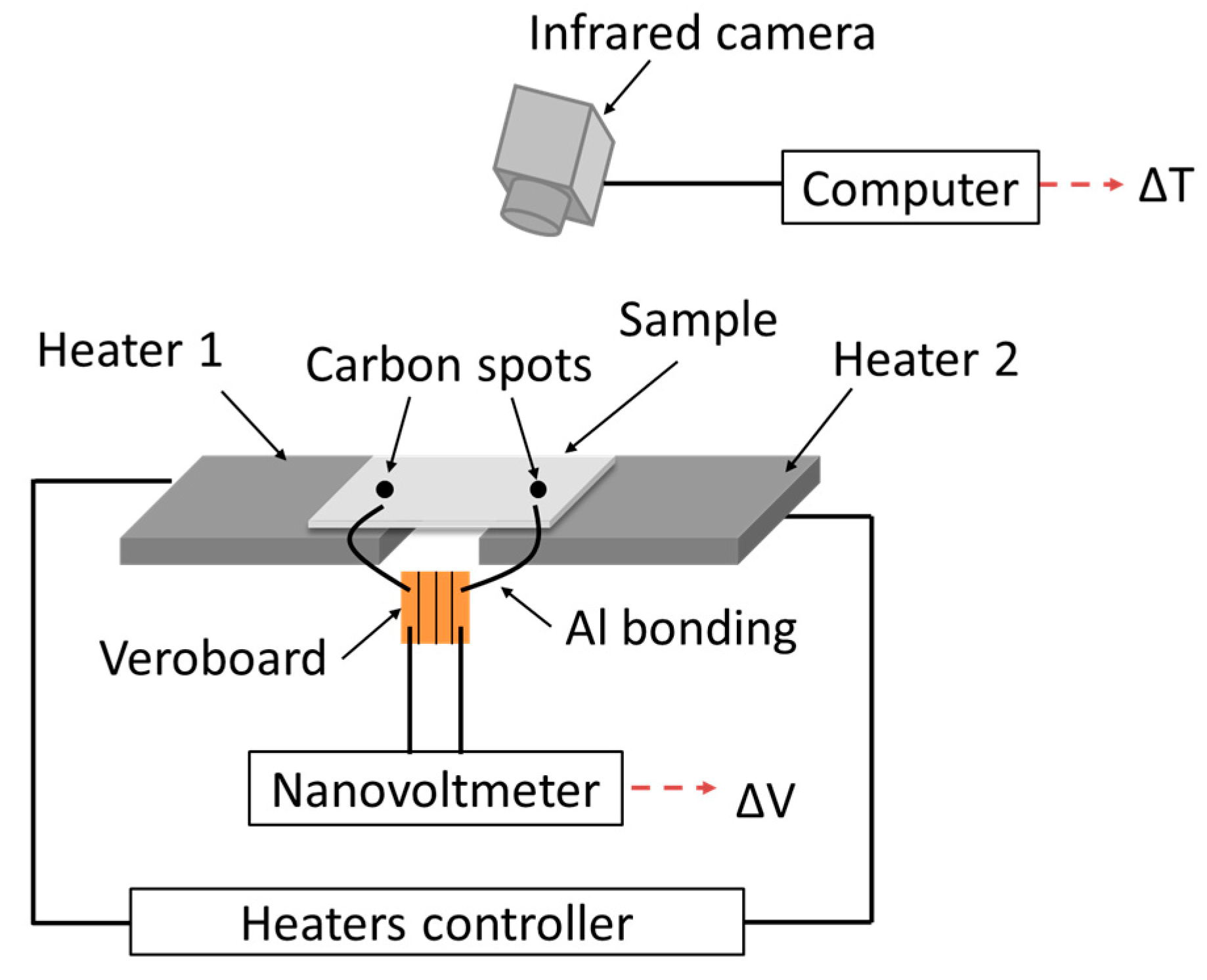
2.3. Characterization

The structural properties of the films were investigated by a α = 1° grazing incidence X-ray diffraction (GIXRD) at room temperature. GIXRD was performed using a Siemens D5000 diffractometer equipped with a Bruker Sol-X detector (Siemens, Pittsburgh, PA, USA). Copper radiations were used as X-ray source (λCuKα1 = 1.5405 Å and λCuKα2 = 1.5445 Å). The microstructure of the films was observed using a Nanoscope III Dimension 3000 Atomic Force Microscope (AFM). AFM surface views were analyzed using the Gwyddion software. The band gap energy has been determined by the measure of the total transmittance and the total reflectance in the 300 to 1100 nm wavelength range using a Bentham PVE300 integrated spectrophotometer (Bentham Instruments Ltd., Berkshire, UK).
The electrical resistivity was measured using a four-point probe measurement unit (Signatone, Gilroy, CA, USA).
A home-made measurement setup has been used for the Seebeck coefficient determination as a function of temperature (Figure 1). Two independent heaters fitted to the thin film geometry have been used to apply a thermal gradient along the thin film. Electrical contacts were done with a 25 µm diameter aluminum wire bonder (HYBOND Model 626, Hybond, Escondido, CA, USA). The ohmic type behavior (linearity of current vs. voltage curve) of the electrical contacts has been checked systematically for all samples with a source meter (Keithley 2450, Tektronix, Beaverton, OR, USA) after bonding step. During the experiment, the voltage was measured with a nanovoltmeter (Keithley 2182A, Tektronix, Beaverton, OR, USA). Two carbon spots (emissivity coefficient of 0.97) were deposited on the surface of the thin films by spraying carbon solution through a shadow mask to accurately measure the surface temperature with an infrared camera. The two carbon spots were located at the same isotherm position than the electrical contacts. The mean temperature (TMean) was considered as the average between the temperature of the hot side (THot) and that of the cold side (TCold).
The Seebeck coefficient S(TMean) at a given mean temperature can be calculated with
S ( T Mean ) = S ref Δ V Δ T
where Sref, ΔV, and ΔT are respectively Seebeck coefficient of the reference (Aluminum probe: S = 3.5 µV·K−1), electric potential and temperature difference (THotTCold) measured on the film. The accuracy of the experimental setup was checked by using a bar of Ca3Co4O9 already measured elsewhere with a ZEM3 commercial apparatus. The results were similar with a standard deviation of 7%.

3. Results and Discussion

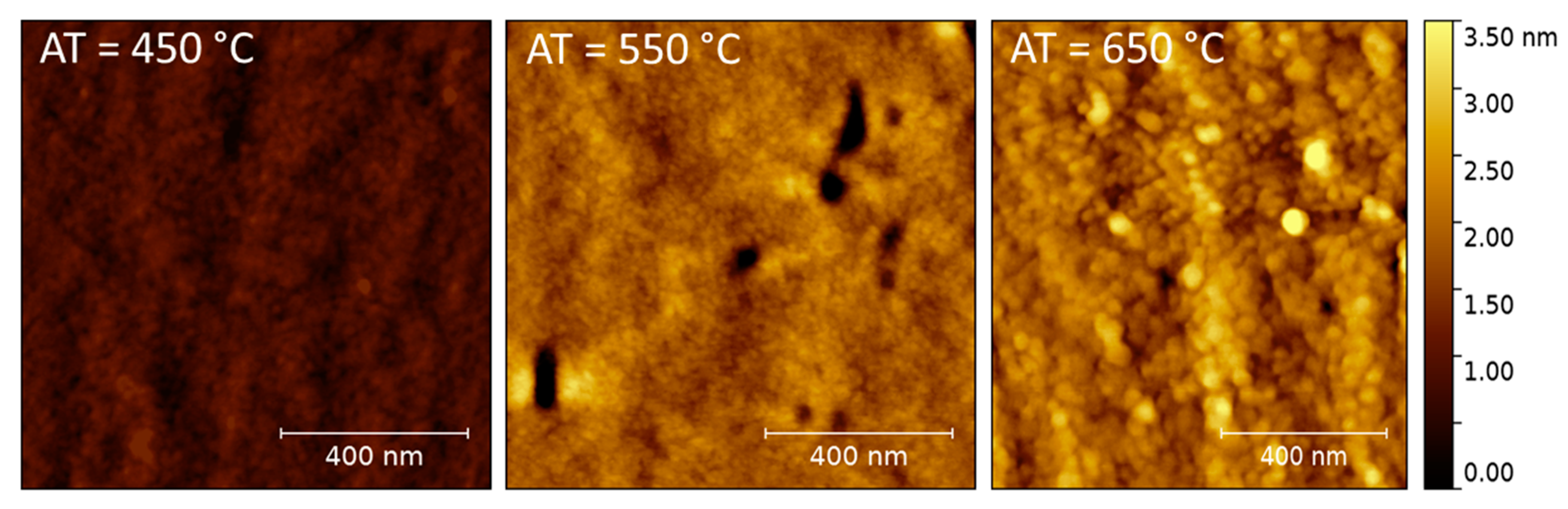
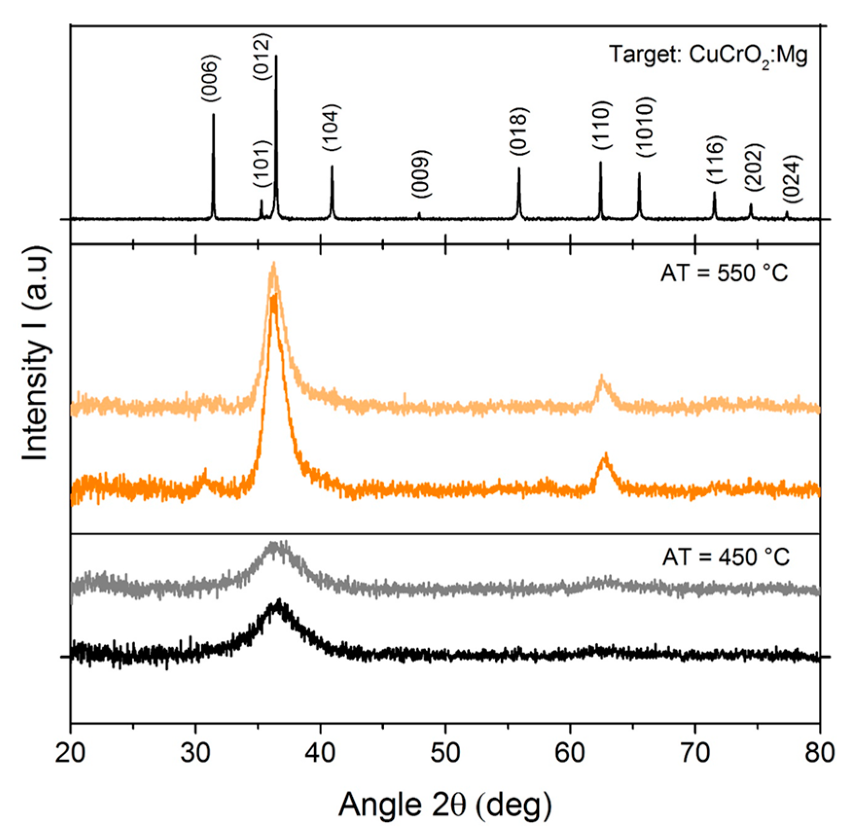
3.1. Structural and Microstructural Characterizations

The GIXRD patterns of CuCrO2:Mg thin films annealed for 4 h at various temperature in the 450 to 650 °C temperature range under primary vacuum have been measured for all samples. The as-deposited sample and the sample annealed at 450 °C were amorphous or nanocrystallized. The samples annealed above 500 °C corresponded to the target pattern of CuCrO2 verifying the rhombohedral R-3m space group [87] (Figure 2). The full width at half maximum (FWHM) for the peak (012) decreased strongly with increasing annealing temperature (AT), up to 550 °C. For AT above 550 °C, the FWHM value was stable. As the instrumental contribution and the micro-strain are constant or negligible, it means that grain growth mainly occurred between 450 and 550 °C. The GIXRD pattern of the sample annealed at 450 and 550 °C were shown as an example in the Figure 2. All the characteristic Bragg peaks of the 3R delafossite phase are reported (PC-PDF file #39-0247). It confirms that the experimental conditions used to elaborate the samples provided a pure CuCrO2:Mg phase. The lattice parameters determined by profile matching with constant scale factor were a = 2.96(7) Å and c = 17.14(5) Å.
In order to check the stability of the delafossite phase during the various measurements in temperature, a GIXRD analysis was done after a thermal treatment at 240 °C under air atmosphere for all samples. The result (Figure 2) shows similar patterns before (dark color) and after the thermal treatment for thin film initially annealed at 450 and 550 °C (light color). Thus, there were no additional phases formed during the physical characterization in temperature from room temperature to 220 °C in air atmosphere.
The AFM analysis of the CuCrO2:Mg annealed at 450, 550, and 650 °C reveals the microstructure of the thin films (Figure 3). They exhibit nanocrystallized surfaces. The results show a smooth surface for the 450 °C and 550 °C annealed films and for 650 °C annealed film, the grains are well-defined. Hence, the AFM results are in perfect agreement with the GIXRD analysis.

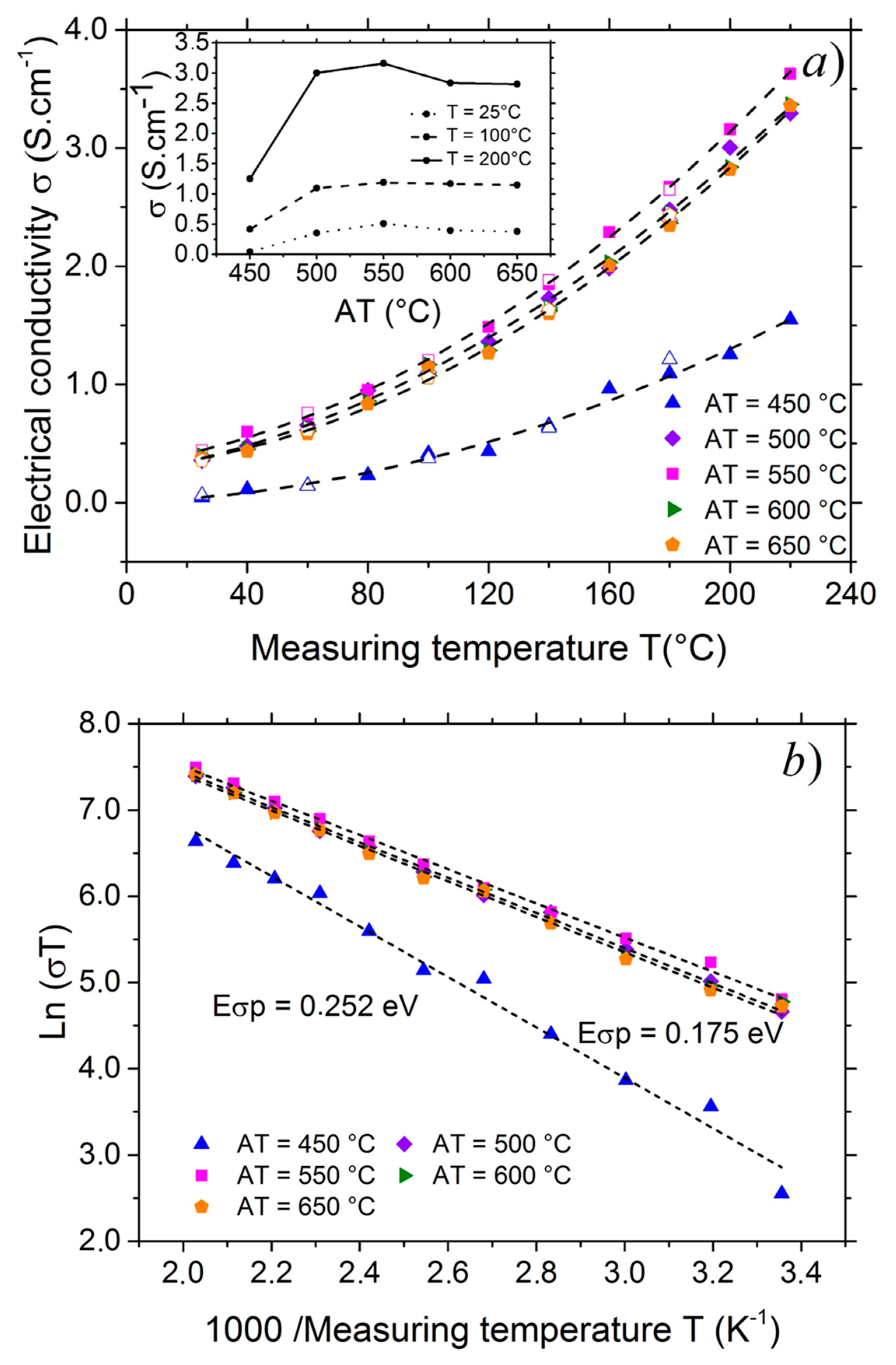
3.2. Transport Properties

The inset of the Figure 4a shows the electrical conductivity σ, at three measuring temperatures, of the 300 nm thick films as a function of the annealing temperature (AT). The as-deposited sample had the lowest electrical conductivity (at room temperature σas-deposited = 6.10−3 S·cm−1). This electrical conductivity measured at room temperature increased with the annealing temperature from 450 to 550 °C and reached 0.51 S·cm−1 then decreased slightly for higher annealing temperatures. Similar decrease of the electrical conductivity has already been observed by various authors and attributed to the decrease of copper vacancies and oxygen interstitials at higher temperatures [75,88] or microstructural changes [16]. In the literature, the electrical conductivity of CuCrO2:Mg films ranged from 0.033 to 1.6 S·cm−1 [16,78,83,84,89,90]. For 305 nm thick CuCrO2:Mg films, Rastogi et al. [84] found 0.1–0.2 S·cm−1 whereas, higher electrical conductivity of 0.6–1 S·cm−1 was obtained for 155 nm thick films. Their results are consistent with the present study.
The Figure 4a,b shows the variation of the electrical conductivity of the CuCrO2:Mg films with the measuring temperature. The electrical measurements showed that the variation of the electrical conductivity was fully reversible and increased with temperature as with semiconducting oxides.
For a semiconductor, the relation of the electrical conductivity with the temperature can be written in two ways considering that thermal energy is enough to activate the carriers (corresponding to the classical conduction mode) or not (corresponding to the hopping mechanism). In the second case, the thermal energy activates the small polarons and σ can be expressed as Equation (3). CuCrO2 is known as a polaronic material where the transport mechanism is limited by small polaron hopping (SPH) [72,91,92,93,94].
In the case of small polarons, the expression of electrical conductivity is given by Mott and Davis [95]
σ = A σ p T e E σ p k B T
where Aσp is a constant, Eσp is the activation energy of polaronic conduction.
In order to calculate the activation energy Eσp using SPH model, we plotted ln(σT) versus 1000/T in the Figure 4b. The results showed a linear variation and the slope of the lines gave Eσp/kB. It is found that the polaronic activation energy decreased when annealing was carried out above 500 °C and reached a quasi-constant value close to 175 meV.

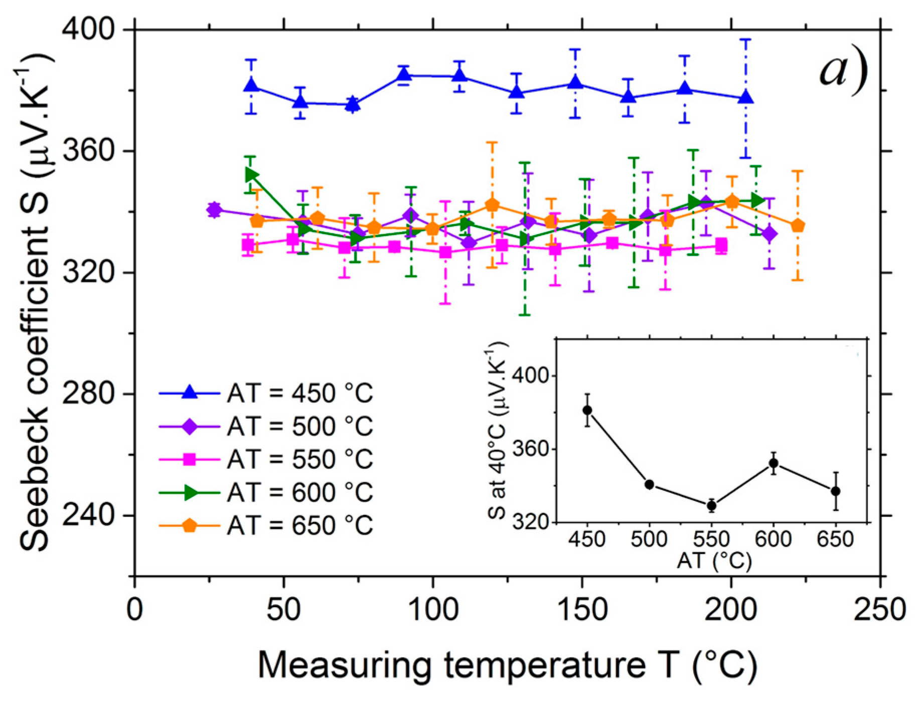
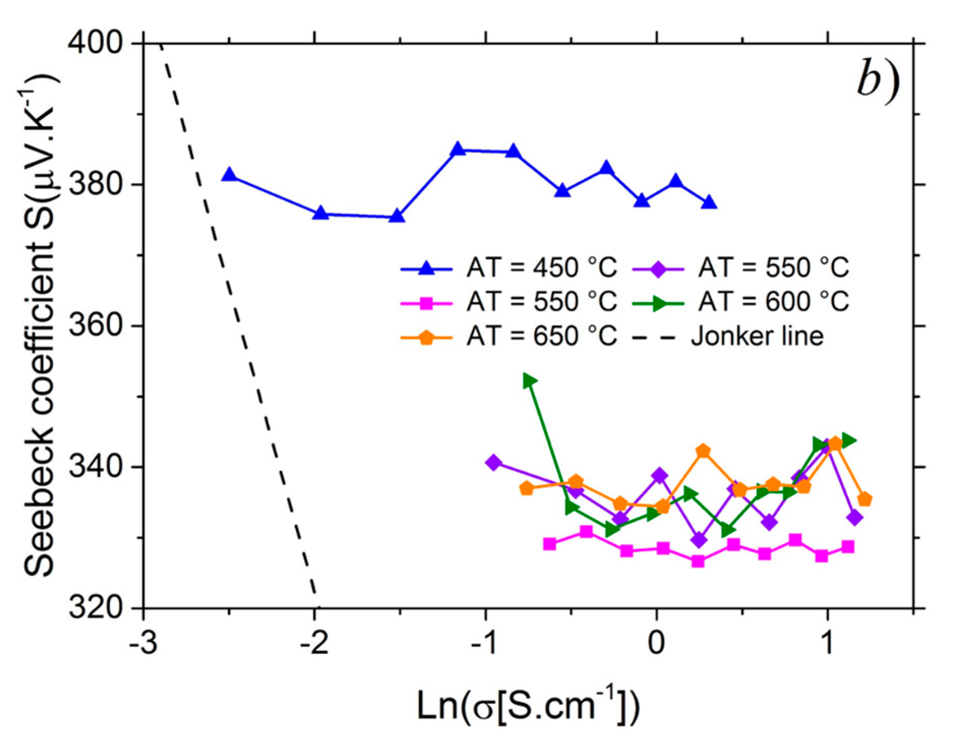
3.3. Seebeck Coefficient Measurement

The Figure 5a shows the Seebeck coefficient of the films as a function of the measuring temperature. The positive values of Seebeck coefficient confirmed that the CuCrO2:Mg films were p-type semiconductors for all annealing temperatures. The lowest Seebeck coefficient was obtained for the highest electrical conductivity due to the carrier density variation. The measurement temperature, from 40 to 220 °C, did not influence the Seebeck coefficient. In the literature, the Seebeck coefficient of CuCrO2:Mg bulk is ranging between 200–500 µV·K−1 and does not vary a lot with temperature in the 77 to 827 °C range [69,70,79] which is coherent with the present Seebeck measurements. Tripathi et al. [82] reported comparable value (≃+300 µV·K−1 at room temperature) for undoped CuCrO2 films. On the other hand, Chikoidze et al. [83] published three times lower value of Seebeck coefficient (+130 µV·K−1 at 23 °C) for 4% Mg doped CuCrO2 thin film. Overall, trends are similar and the difference in values could be explained by the difference in the measurement setup and the material type.
The invariance of Seebeck coefficient in temperature indicates that the hole density is constant between 40 and 220 °C. Therefore, the increase in electrical conductivity is the consequence of the increase in small polarons mobilities due to the hopping mechanism. In the classical conduction mode within the saturation regime, the electrical conductivity would have decreased because of the carrier mobility diminution ( μ T 3 2 ).
Jonker relation (Equation (4)) shows that Jonker plot S versus ln(σ) would have a slope kB/q = ±86.17 µV·K−1 indicating the thermally activated non-degenerate semiconductor behavior (free carrier).
S = ± k B q ( ln σ ln σ 0 )
The plotted curves of the films in the inset of the Figure 5b were far away from the Jonker line. Consequently the Jonker plot S versus ln(σ) [96] showed a degenerate semiconductor behavior for the whole samples. Chikoidze et al. [83] noticed the quasi invariance of the Seebeck coefficient with the measurement temperature, which is consistent with the present results. Farrell et al. [72] also reported degenerate behavior for Cu deficient CuCrO2 film.

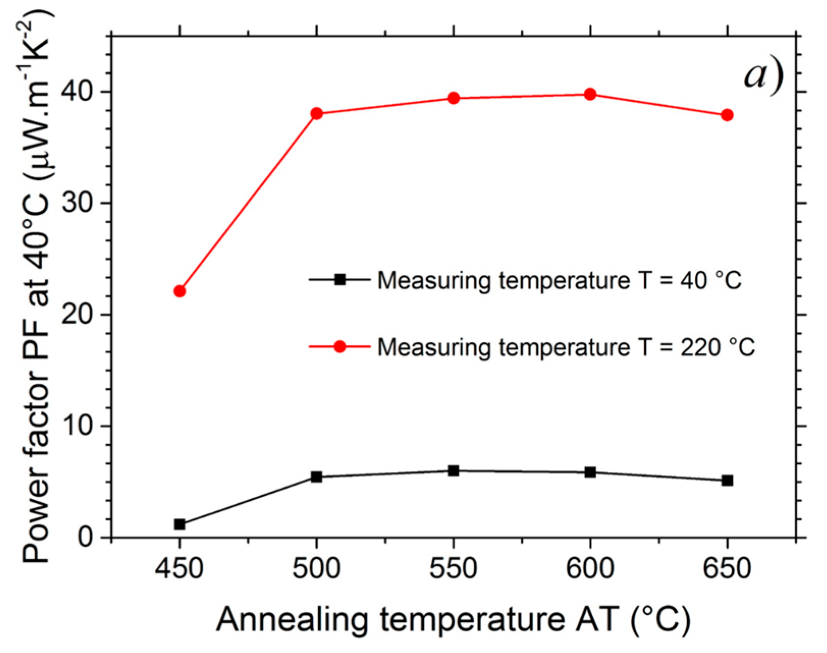
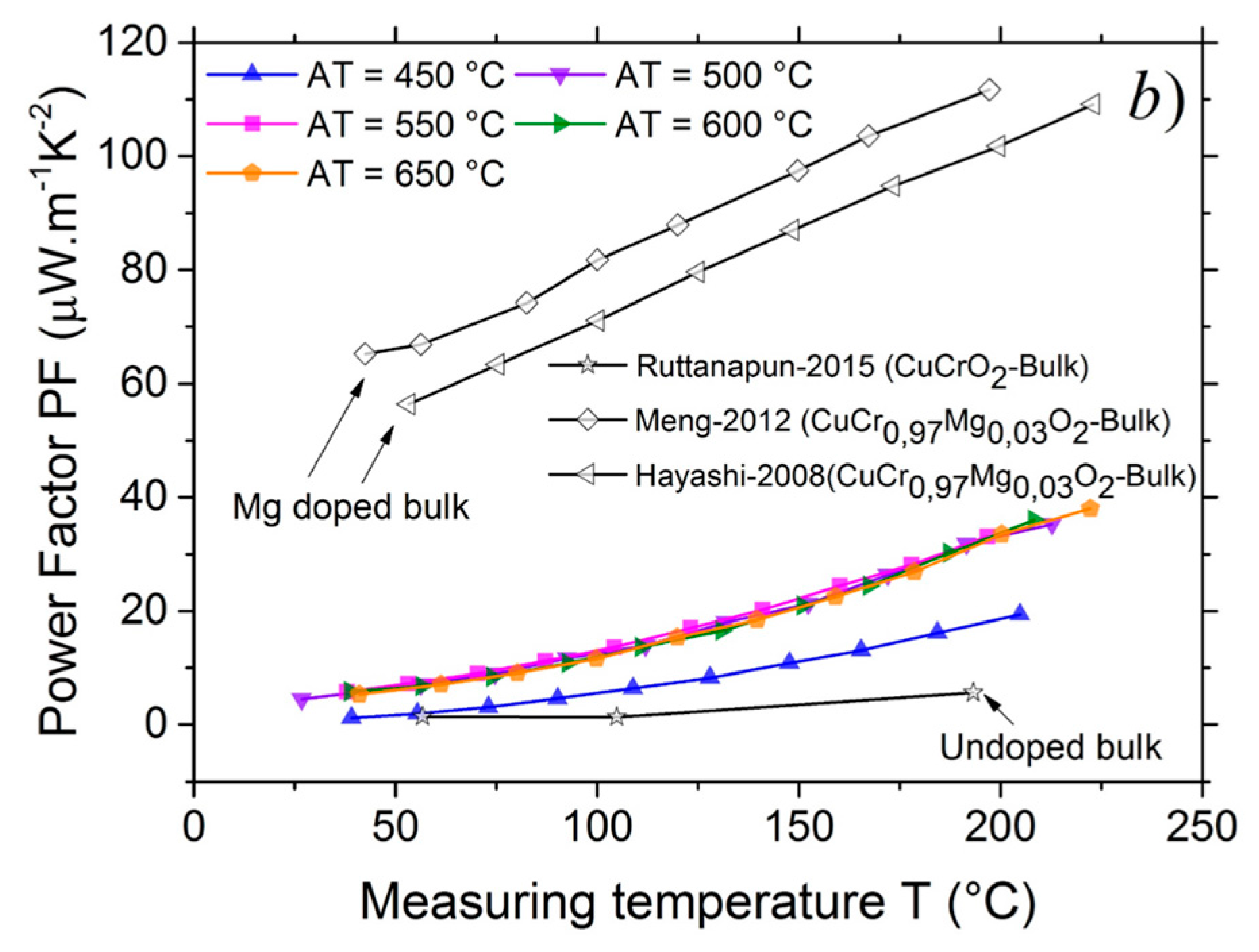
3.4. Power Factor (PF)

The PF values were calculated from the electrical conductivity and the Seebeck coefficient (PF = σS2). The Figure 6a shows the variation of the PF at 40 °C as a function of the annealing temperature and the highest PF is obtained for samples annealed between 550 and 600 °C. The Figure 6b shows the power factor (PF) for the CuCrO2:Mg films annealed at different temperatures, as a function of the measuring temperature and gives a comparison with the data from the literature. As the Seebeck coefficient was quasi constant with increasing temperature, the PF followed the electrical conductivity variation. It increased with increasing measurement temperature. Around 220 °C, it reached 38 µW·m−1·K−2. CuCrO2:Mg films had a higher PF than the CuCrO2 bulk studied by Ruttanapun et al. [80]. However, their PF were lower than the experimentally achieved PF of CuCrO2:Mg bulk materials [69]. For example, Q. Meng et al. found 65 µW·m−1·K−2 at 40 °C for CuCrO2:Mg bulk material [79] thanks to the high electrical conductivity. In comparison with the PF obtained with bulk material, a slight improvement of the power factor of CuCrO2:Mg in the form of thin film could still be achieved by optimizing the film nanostructuration. Moreover, the thickness of the films deposited by RF-magnetron sputtering were 300 nm and showed columnar nanometric grains [16] which implies a lower thermal conductivity due to phonon boundary scattering without reducing the electrical conductivity.
The main advantage of the thin film compared to the bulk is noticeable with the figure of merit ZT where the thermal conductivity is taken into account. Indeed, the lattice thermal conductivity in thin films is generally lower than the bulk materials [2,7,8]. However, in this work, the values for ZT have not been calculated because the thermal conductivity of CuCrO2:Mg in the form of thin films could not be measured.

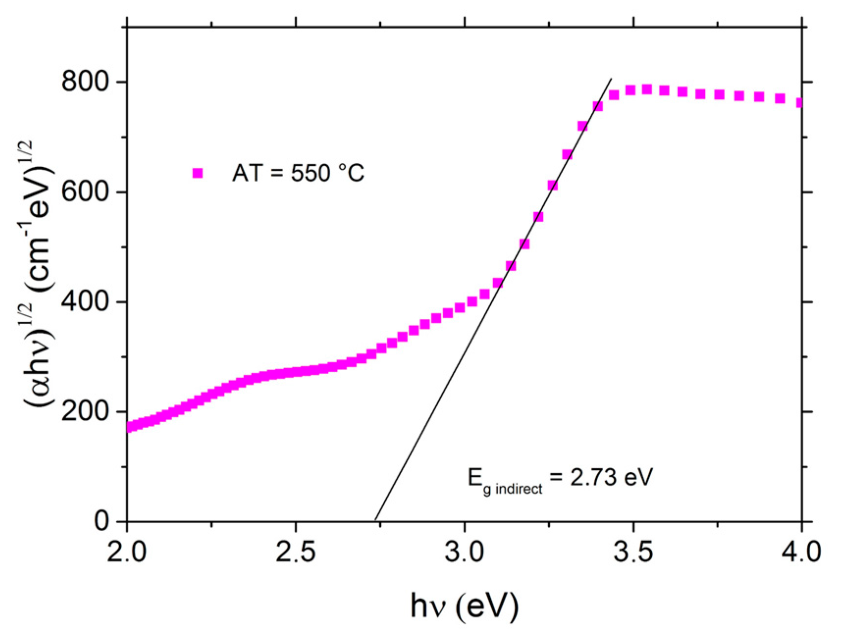
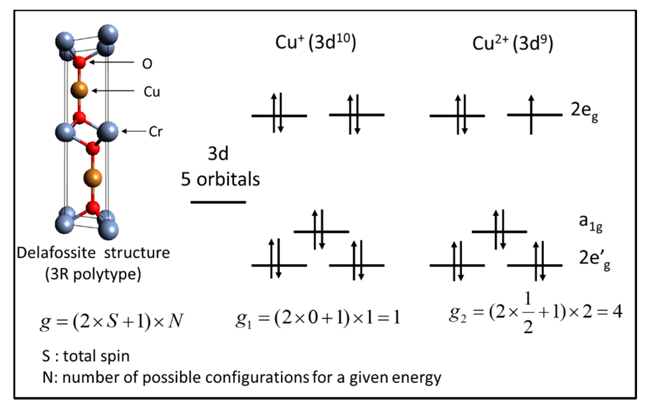
3.5. Optoelectrical Properties and Fermi Energy Level

The fundamental indirect band gap energy was determined by the measurements of the total transmittance TT (specular and diffuse) and the total reflectance TR (not shown here). The Tauc’s plot [97] gives the optical fundamental band gap from the linear extrapolation of the curve slope to intercept the energy axis (Figure 7). In detail, the absorption coefficient α, was estimated from the relation [98]
α = 1 d ln ( ( 1 T R ) 2 T T )
where d is the film thickness. The fundamental indirect band gap energy was determined using the absorption coefficient α via the relation
( α h υ ) m = A ( h υ E g )
where hν is the photon energy, Eg is the optical band gap, A is a constant called the band tailing parameter and m = 1/2 for the fundamental indirect transition. Using the Tauc’s method, 2.73 eV was obtained for the fundamental indirect transition (Figure 7). The obtained energy value is consistent with the literature [84] and shows a wide band gap which avoids the simultaneous presence of the electron and hole in their specific bands and drives to a high Seebeck coefficient even at high temperatures. A similar indirect band gap value was obtained by Chikoidze et al. [83] and Kaya et al. [99].
The Fermi energy was calculated using the following Mott formula [100] for a degenerate electron gas approximation
S π 2 k B 2 T 3 q E F
In this case, the Fermi energy is taken from the valence band edge. At 40 °C, the Fermi energy value was 0.022 ± 0.002 eV which is lower than the thermal energy (3kBT = 0.081 eV at 314 K) on the Fermi distribution width. It leads to the conclusion that the samples did not display thermally activated characteristics, which is consistent for a degenerate semiconductor. The Fermi level can trace the work function of the delafossite and give precious information about which metal can be used for ohmic contact (to avoid the Schottky barriers) with the delafossite. This information is needed for the thermoelectric, optoelectronic, and photocatalytic applications.

3.6. Carrier Concentration and Hole Effective Mass

According to the Hubbard model [101] and Heike’s formula [102] adapted for degenerate semiconductor with a carrier hopping mechanism, the Seebeck coefficient can be written as Equation (8)
S = + k B q ln [ ( g 1 g 2 ) [ C u + ] [ C u 2 + ] ]
where g is the spin and orbital degeneracy and [Cu+]/[Cu2+] is the ratio of the ion concentrations.
At high temperature, due to the mixed valences of the copper (Cu+/Cu2+) in the CuCrO2:Mg, the Seebeck coefficient which is the measure of the entropy of the carriers is given by the spin and orbital degeneracy [73]. The Figure 8 shows the spin and orbital degeneracies of Cu+ (g1) and Cu2+ (g2) due to Mg2+ doping compensation according to (Cu+1−xCu2+x)(Cr3+1−xMg2+x)O2 in the linear bonding O–Cu–O (where the coordination number of Cu is 2). Thereby, from the measured Seebeck coefficient, the concentration of Cu+ and Cu2+ ions have been estimated and they varied barely with the annealing temperature (AT). The obtained values were [Cu+] = 0.995 and [Cu2+] = 0.005 for AT above 500 °C.
Using the unit cell volumes determined by the GIXRD measurements, the density of total copper site dCu in the delafossite structure is estimated at (2.30 ± 0.02) × 1022 cm−3. The hole density which is related to the Cu2+ concentration is equal to dCu × [Cu2+] = (1.17 ± 0.05) × 1020 cm−3.
The hole effective mass, m*, was calculated using the equation
m * = 2 2 E F ( 3 π 2 h s ) 2 / 3
where ћ is the reduced Planck constant and hs is the hole density.
The hole effective mass estimated for CuCrO2:Mg was 3.80 ± 0.2 m0 which is close to the effective mass predicted theoretically for CuCrO2 by Scanlon et al. [103] (without spin-orbit coupling m*th = 2.96 m0 and with spin-orbit coupling m*th = 4.53 m0).
The effective hole mass is rarely published for this type of material. However, it is requisite for the optoelectronic application in particular for the determination of the hole mobility.

4. Conclusions

CuCrO2:Mg thin films have been elaborated by RF magnetron sputtering and annealed at different temperatures between 450 and 650 °C under primary vacuum. The as-deposited film and the film annealed at 450 °C were nanocrystalized, whereas the films annealed above 500 °C had a delafossite structure. The AFM has shown a nanometric grains sizes and smooth surface at the optimal annealing temperature. The higher electrical conductivity determined at 40 °C was 0.60 S·cm−1 for the film annealed at 550 °C which had a Seebeck coefficient of +329 µV·K−1. We analyzed the small polaron hopping conductivity mechanism and found a degenerate semiconductor behavior of the CuCrO2:Mg thin films. Thanks to its constant Seebeck coefficient between 40 and 220 °C and high fundamental indirect band gap energy, the power factor increased like the electrical conductivity when the temperature was increased, and reached 38 µW·m−1·K−2 at 220 °C. CuCrO2:Mg thin films have been studied for their TE properties and showed encouraging results. Their high and constant Seebeck coefficient in changing temperatures and their stability in air atmosphere could be a great advantage for an application of this material in high accuracy temperature measurement devices, miniaturized devices in thin film configuration, and also transparent TE devices due to its TCO properties.

Acknowledgments

The authors would like to thank the French ministry of Research for the National PhD funding.

Author Contributions

I. Sinnarasa has deposited and characterized the thin films and wrote the paper. Y. Thimont is the coordinated of this research work, he processed and analyzed the TE properties and developed the TE measurement setup devoted to the thin films geometry, he has contributed to the paper writing. L. Presmanes has contributed to the sputtering parameters optimization and the nanostructuration characterization. A. Barnabé and P. Tailhades have characterized the structure of the delafossite thin films.

Conflicts of Interest

The authors declare no conflict of interest.

References

  1. Rowe, D.M. CRC Handbook of Thermoelectrics; CRC Press: Boca Raton, FL, USA, 1995. [Google Scholar]
  2. Alam, H.; Ramakrishna, S. A review on the enhancement of figure of merit from bulk to nano-thermoelectric materials. Nano Energy 2013, 2, 190–212. [Google Scholar] [CrossRef]
  3. Martin, J.; Tritt, T.; Uher, C. High temperature Seebeck coefficient metrology. J. Appl. Phys. 2010, 108, 121101. [Google Scholar] [CrossRef]
  4. Aswal, D.K.; Basu, R.; Singh, A. Key issues in development of thermoelectric power generators: High figure-of-merit materials and their highly conducting interfaces with metallic interconnects. Energy Convers. Manag. 2016, 114, 50–67. [Google Scholar] [CrossRef]
  5. Dresselhaus, M.S.; Chen, G.; Tang, M.Y.; Yang, R.G.; Lee, H.; Wang, D.Z.; Ren, Z.F.; Fleurial, J.-P.; Gogna, P. New Directions for Low-Dimensional Thermoelectric Materials. Adv. Mater. 2007, 19, 1043–1053. [Google Scholar] [CrossRef]
  6. Chen, Z.-G.; Han, G.; Yang, L.; Cheng, L.; Zou, J. Nanostructured thermoelectric materials: Current research and future challenge. Prog. Nat. Sci. Mater. Int. 2012, 22, 535–549. [Google Scholar] [CrossRef]
  7. Cahill, D.G.; Fischer, H.E.; Klitsner, T.; Swartz, E.T.; Pohl, R.O. Thermal conductivity of thin films: Measurements and understanding. J. Vac. Sci. Technol. A Vac. Surf. Films 1989, 7, 1259–1266. [Google Scholar] [CrossRef]
  8. Loureiro, J.; Santos, J.R.; Nogueira, A.; Wyczisk, F.; Divay, L.; Reparaz, S.; Alzina, F.; Sotomayor Torres, C.M.; Cuffe, J.; Montemor, F.; et al. Nanostructured p-type Cr/V2O5 thin films with boosted thermoelectric properties. J. Mater. Chem. A 2014, 2, 6456–6462. [Google Scholar] [CrossRef]
  9. Venkatasubramanian, R.; Siivola, E.; O’Quinn, B.; Coonley, K.; Colpitts, T.; Addepalli, P.; Napier, M.; Mantini, M. Nanostructured Superlattice Thin-Film Thermoelectric Devices. In Nanotechnology and the Environment; ACS Symposium Series; American Chemical Society: Washington, DC, USA, 2004; pp. 347–352. [Google Scholar]
  10. Benko, F.A.A.; Koffyberg, F.P.P. Preparation and opto-electronic properties of semi-conducting CuCrO2. Mater. Res. Bull. 1986, 21, 753–757. [Google Scholar] [CrossRef]
  11. Kawazoe, H.; Yasukawa, M.; Hyodo, H.; Kurita, M.; Yanagi, H.; Hosono, H. p-type electrical conduction in transparent thin films of CuAlO2. Nature 1997, 389, 939–942. [Google Scholar] [CrossRef]
  12. Nagarajan, R.; Duan, N.; Jayaraj, M.K.; Li, J.; Vanaja, K.A.; Yokochi, A.; Draeseke, A.; Tate, J.; Sleight, A.W. p-Type conductivity in the delafossite structure. Int. J. Inorg. Mater. 2001, 3, 265–270. [Google Scholar] [CrossRef]
  13. Yanagi, H.; Hase, T.; Ibuki, S.; Ueda, K.; Hosono, H. Bipolarity in electrical conduction of transparent oxide semiconductor CuInO2 with delafossite structure. Appl. Phys. Lett. 2001, 78, 1583–1585. [Google Scholar] [CrossRef]
  14. Banerjee, A.N.; Chattopadhyay, K.K. Recent developments in the emerging field of crystalline p-type transparent conducting oxide thin films. Prog. Cryst. Growth Charact. Mater. 2005, 50, 52–105. [Google Scholar] [CrossRef]
  15. Stadler, A. Transparent Conducting Oxides-An Up-To-Date Overview. Materials 2012, 5, 661–683. [Google Scholar] [CrossRef]
  16. Barnabé, A.; Thimont, Y.; Lalanne, M.; Presmanes, L.; Tailhades, P. P-type conducting transparent characteristics of delafossite Mg-doped CuCrO2 thin films preparation by RF-sputtering. J. Mater. Chem. C 2015, 3, 6012–6024. [Google Scholar] [CrossRef]
  17. Zhang, K.H.L.; Xi, K.; Blamire, M.G.; Egdell, R.G. P-type transparent conducting oxides. J. Phys. Condens. Matter 2016, 28, 383002. [Google Scholar] [CrossRef] [PubMed]
  18. Barquinha, P.; Martins, R.; Pereira, L.; Fortunato, E. Transparent Oxide Electronics: From Materials to Devices; John Wiley & Sons, Ltd.: Hoboken, NJ, USA, 2008. [Google Scholar]
  19. Wager, J.F.; Kesler, D.A.; Presley, D.A. Transparent Electronics; Springer: New York, NY, USA, 2008. [Google Scholar]
  20. Tonooka, K.; Kikuchi, N. Preparation of transparent CuCrO2: Mg/ZnO p-n junctions by pulsed laser deposition. Thin Solid Films 2006, 515, 2415–2418. [Google Scholar] [CrossRef]
  21. Hosono, H.; Ota, H.; Kawamura, K.; Sarukura, N.; Hirano, M. Light-Emitting Diode and Laser Diode Having N-Type ZnO Layer and P-Type Semiconductor Laser. U.S. Patent 6,806,503, 19 October 2004. [Google Scholar]
  22. Yanagi, H.; Ueda, K.; Ohta, H.; Orita, M.; Hirano, M.; Hosono, H. Fabrication of all oxide transparent p-n homojunction using bipolar CuInO2 semiconducting oxide with delafossite structure. Solid State Commun. 2002, 121, 15–18. [Google Scholar] [CrossRef]
  23. Ling, B.; Zhao, J.L.; Sun, X.W.; Tan, S.T.; Kyaw, A.K.K.; Divayana, Y.; Dong, Z.L. Color tunable light-emitting diodes based on p+-Si/p-CuAlO2 /n-ZnO nanorod array heterojunctions. Appl. Phys. Lett. 2010, 97, 13101. [Google Scholar] [CrossRef]
  24. Chiu, T.W.; Tonooka, K.; Kikuchi, N. Fabrication of ZnO and CuCrO2: Mg thin films by pulsed laser deposition with in situ laser annealing and its application to oxide diodes. Thin Solid Films 2008, 516, 5941–5947. [Google Scholar] [CrossRef]
  25. Tate, J.; Jayaraj, M.K.K.; Draeseke, A.D.D.; Ulbrich, T.; Sleight, A.W.W.; Vanaja, K.A.; Nagarajan, R.; Wager, J.F.F.; Hoffman, R.L.L. p-Type oxides for use in transparent diodes. Thin Solid Films 2002, 411, 119–124. [Google Scholar] [CrossRef]
  26. Renaud, A.; Cario, L.; Deniard, P.; Gautron, E.; Rocquefelte, X.; Pellegrin, Y.; Blart, E.; Odobel, F.; Jobic, S. Impact of Mg Doping on Performances of CuGaO2 Based p-Type Dye-Sensitized Solar Cells. J. Phys. Chem. C 2014, 118, 54–59. [Google Scholar] [CrossRef]
  27. Asemi, M.; Ghanaatshoar, M. Hydrothermal growth of one-dimensional Ce-doped TiO2 nanostructures for solid-state DSSCs comprising Mg-doped CuCrO2. J. Mater. Sci. 2017, 52, 489–503. [Google Scholar] [CrossRef]
  28. Zhu, T.; Deng, Z.; Fang, X.; Huo, Z.; Wang, S.; Dong, W.; Shao, J.; Tao, R.; Song, C.; Wang, L. High photovoltages of CuFeO2 based p-type dye-sensitized solar cells. J. Alloys Compd. 2016, 685, 836–840. [Google Scholar] [CrossRef]
  29. Jiang, T.; Bujoli-Doeuff, M.; Farré, Y.; Blart, E.; Pellegrin, Y.; Gautron, E.; Boujtita, M.; Cario, L.; Odobel, F.; Jobic, S. Copper borate as a photocathode in p-type dye-sensitized solar cells. RSC Adv. 2016, 6, 1549–1553. [Google Scholar] [CrossRef]
  30. Wuttig, A.; Krizan, J.W.; Gu, J.; Frick, J.J.; Cava, R.J.; Bocarsly, A.B. The effect of Mg-doping and Cu nonstoichiometry on the photoelectrochemical response of CuFeO2. J. Mater. Chem. A 2017, 5, 165–171. [Google Scholar] [CrossRef]
  31. Toyoda, K.; Hinogami, R.; Miyata, N.; Aizawa, M. Calculated Descriptors of Catalytic Activity for Water Electrolysis Anode: Application to Delafossite Oxides. J. Phys. Chem. C 2015, 119, 6495–6501. [Google Scholar] [CrossRef]
  32. Carcia, P.F.; Shannon, R.D.; Bierstedt, P.E.; Flippen, R.B. Oxygen electrocatalysis on Thin Film Metallic Oxide Electrodes with the Delafossite Structure. J. Electrochem. Soc. 1980, 127, 1974. [Google Scholar] [CrossRef]
  33. Dong, H.; Li, Z.; Xu, X.; Ding, Z.; Wu, L.; Wang, X.; Fu, X. Visible light-induced photocatalytic activity of delafossite AgMO2 (M=Al, Ga, In) prepared via a hydrothermal method. Appl. Catal. B Environ. 2009, 89, 551–556. [Google Scholar] [CrossRef]
  34. Ketir, W.; Rekhila, G.; Trari, M.; Amrane, A. Preparation, characterization and application of CuCrO2/ZnO photocatalysts for the reduction of Cr(VI). J. Environ. Sci. 2012, 24, 2173–2179. [Google Scholar] [CrossRef]
  35. Saadi, S.; Bouguelia, A.; Trari, M. Photocatalytic hydrogen evolution over CuCrO2. Sol. Energy 2006, 80, 272–280. [Google Scholar] [CrossRef]
  36. Rao, R.; Dandekar, A.; Baker, R.T.K.; Vannice, M.A. Properties of Copper Chromite Catalysts in Hydrogenation Reactions. J. Catal. 1997, 171, 406–419. [Google Scholar] [CrossRef]
  37. Koriche, N.; Bouguelia, A.; Aider, A.; Trari, M. Photocatalytic hydrogen evolution over delafossite. Int. J. Hydrog. Energy 2005, 30, 693–699. [Google Scholar] [CrossRef]
  38. Ketir, W.; Bouguelia, A.; Trari, M. Visible Light Induced NO2 (-) Removal Over CuCrO2 Catalyst. Water Air Soil Pollut. 2009, 199, 115–122. [Google Scholar] [CrossRef]
  39. Zhang, P.; Shi, Y.; Chi, M.; Park, J.N.; Stucky, G.D.; McFarland, E.W.; Gao, L. Mesoporous delafossite CuCrO2 and spinel CuCr2O4: Synthesis and catalysis. Nanotechnology 2013, 24, 345704. [Google Scholar] [CrossRef] [PubMed]
  40. Jang, Y.J.; Park, Y.B.; Kim, H.E.; Choi, Y.H.; Choi, S.H.; Lee, J.S. Oxygen-Intercalated CuFeO2 Photocathode Fabricated by Hybrid Microwave Annealing for Efficient Solar Hydrogen Production. Chem. Mater. 2016, 28, 6054–6061. [Google Scholar] [CrossRef]
  41. Lekse, J.W.; Underwood, M.K.; Lewis, J.P.; Matranga, C. Synthesis, Characterization, Electronic Structure, and Photocatalytic Behavior of CuGaO2 and CuGa1−xFexO2(x = 0.05, 0.10, 0.15, 0.20) Delafossites. J. Phys. Chem. C 2012, 116, 1865–1872. [Google Scholar] [CrossRef]
  42. Chiu, T.W.; Yang, Y.C.; Yeh, A.C.; Wang, Y.P.; Feng, Y.W. Antibacterial property of CuCrO2 thin films prepared by RF magnetron sputtering deposition. Vacuum 2013, 87, 174–177. [Google Scholar] [CrossRef]
  43. Doumerc, J.P.; Parent, C.; Chao, Z.J.; Le Flem, G.; Ammar, A. Luminescence of the Cu+ ion in CuLaO2. J. Less Common Met. 1989, 148, 333–337. [Google Scholar] [CrossRef]
  44. Jacob, A.; Parent, C.; Boutinaud, C.; Le Flem, G.; Doumerc, J.P.; Ammar, A.; Elazhari, M.; Elaatmani, M. Luminescent properties of Delafossite-type oxides LaCuO2 and YCuO2. Solid State Commun. 1997, 103, 529–532. [Google Scholar] [CrossRef]
  45. Byrne, D.; Cowley, A.; Bennett, N.; McGlynn, E. The luminescent properties of CuAlO2. J. Mater. Chem. C 2014, 2, 7859–7868. [Google Scholar] [CrossRef]
  46. Patzsch, J.; Balog, I.; Krauß, P.; Lehmann, C.W.; Schneider, J.J. Synthesis, characterization and p–n type gas sensing behaviour of CuFeO2 delafossite type inorganic wires using Fe and Cu complexes as single source molecular precursors. RSC Adv. 2014, 4, 15348. [Google Scholar] [CrossRef]
  47. Elgazzar, E.; Tataroğlu, A.; Al-Ghamdi, A.A.; Al-Turki, Y.; Farooq, W.A.; El-Tantawy, F.; Yakuphanoglu, F. Thermal sensors based on delafossite film/p-silicon diode for low-temperature measurements. Appl. Phys. A 2016, 122, 617. [Google Scholar] [CrossRef]
  48. Zheng, X.G.; Taniguchi, K.; Takahashi, A.; Liu, Y.; Xu, C.N. Room temperature sensing of ozone by transparent p-type semiconductor CuAlO2. Appl. Phys. Lett. 2004, 85, 1728–1729. [Google Scholar] [CrossRef]
  49. Zhou, S.; Fang, X.; Deng, Z.; Li, D.; Dong, W.; Tao, R.; Meng, G.; Wang, T. Room temperature ozone sensing properties of p-type CuCrO2 nanocrystals. Sens. Actuators B 2009, 143, 119–123. [Google Scholar] [CrossRef]
  50. Uhrmacher, M.; Attili, R.N.; Lieb, K.P.; Winzer, K.; Mekata, M. Perturbed Angular Correlation Measurements in 2D Spin-Frustrated CuFeO2. Phys. Rev. Lett. 1996, 76, 4829–4831. [Google Scholar] [CrossRef] [PubMed]
  51. Terada, N.; Mitsuda, S.; Oohara, Y.; Yoshizawa, H.; Takei, H. Anomalous magnetic excitation on triangular lattice antiferromagnet CuFeO2. J. Magn. Magn. Mater. 2004, 272–276, e997–e998. [Google Scholar] [CrossRef]
  52. Hoffman, R.; Wager, J. Transistor Device Having a Delafossite Material. U.S. Patent 7,026,713, 11 April 2006. [Google Scholar]
  53. Maignan, A.; Martin, C.; Frésard, R.; Eyert, V.; Guilmeau, E.; Hébert, S.; Poienar, M.; Pelloquin, D. On the strong impact of doping in the triangular antiferromagnet CuCrO2. Solid State Commun. 2009, 149, 962–967. [Google Scholar] [CrossRef]
  54. O’Sullivan, M.; Stamenov, P.; Alaria, J.; Venkatesan, M.; Coey, J.M.D. Magnetoresistance of CuCrO2-based delafossite films. J. Phys. Conf. Ser. 2010, 200, 052021. [Google Scholar] [CrossRef]
  55. Shu, J.; Zhu, X.; Yi, T. CuCrO2 as anode material for lithium ion batteries. Electrochim. Acta 2009, 54, 2795–2799. [Google Scholar] [CrossRef]
  56. Huang, X.; Ni, C.; Zhao, G.; Irvine, J.T.S. Oxygen storage capacity and thermal stability of the CuMnO2–CeO2 composite system. J. Mater. Chem. A 2015, 3, 12958–12964. [Google Scholar] [CrossRef]
  57. Díaz-García, A.K.; Lana-Villarreal, T.; Gómez, R. Sol–gel copper chromium delafossite thin films as stable oxide photocathodes for water splitting. J. Mater. Chem. A 2015, 3, 19683–19687. [Google Scholar] [CrossRef]
  58. Taddee, C.; Kamwanna, T.; Amornkitbamrung, V. Characterization of transparent superconductivity Fe-doped CuCrO2 delafossite oxide. Appl. Surf. Sci. 2016, 380, 237–242. [Google Scholar] [CrossRef]
  59. Suriwong, T.; Thongtem, T.; Thongtem, S. Thermoelectric and optical properties of CuAlO2 synthesized by direct microwave heating. Curr. Appl. Phys. 2014, 14, 1257–1262. [Google Scholar] [CrossRef]
  60. Hayashi, K.; Nozaki, T.; Kajitani, T. Structure and High Temperature Thermoelectric Properties of Delafossite-Type Oxide CuFe1−xNixO2 (0 ≤ x ≤ 0.05). Jpn. J. Appl. Phys. 2007, 46, 5226–5229. [Google Scholar] [CrossRef]
  61. Park, K.; Ko, K.Y.; Kwon, H.C.; Nahm, S. Improvement in thermoelectric properties of CuAlO2 by adding Fe2O3. J. Alloys Compd. 2007, 437, 1–6. [Google Scholar] [CrossRef]
  62. Isawa, K.; Yaegashi, Y.; Ogota, S.; Nagano, M.; Sudo, S.; Yamada, K.; Yamauchi, H. Thermoelectric power of delafossite-derived compounds, RCuO2 + δ (R = Y, La, Pr, Nd, Sm, and Eu). Phys. Rev. B 1998, 57, 7950–7954. [Google Scholar] [CrossRef]
  63. Banerjee, A.N.; Maity, R.; Ghosh, P.K.; Chattopadhyay, K.K. Thermoelectric properties and electrical characteristics of sputter-deposited P-CuAlO2 thin films. Thin Solid Films 2005, 474, 261–266. [Google Scholar] [CrossRef]
  64. Park, K.; Ko, K.Y.; Seo, W.-S. Thermoelectric properties of CuAlO2. J. Eur. Ceram. Soc. 2005, 25, 2219–2222. [Google Scholar] [CrossRef]
  65. Guilmeau, E.; Maignan, A.; Martin, C. Thermoelectric Oxides: Effect of Doping in Delafossites and Zinc Oxide. J. Electron. Mater. 2009, 38, 1104–1107. [Google Scholar] [CrossRef]
  66. Nozaki, T.; Hayashi, K.; Kajitani, T.; Nozaki, K.; Hayashi, K.; Kajitani, T. Electronic Structure and Thermoelectric Properties of the Delafossite-Type Oxides CuFe1−xNixO2. J. Electron. Mater. 2009, 38, 1282–1286. [Google Scholar] [CrossRef]
  67. Ruttanapun, C. Effects of Pd substitution on the thermoelectric and electronic properties of delafossite Cu1−xPdxFeO2 (x = 0.01, 0.03 and 0.05). J. Solid State Chem. 2014, 215, 43–49. [Google Scholar] [CrossRef]
  68. Powar, S.; Xiong, D.; Daeneke, T.; Ma, M.T.; Gupta, A.; Lee, G.; Makuta, S.; Tachibana, Y.; Chen, W.; Spiccia, L.; et al. Improved Photovoltages for p-Type Dye-Sensitized Solar Cells Using CuCrO2 Nanoparticles. J. Phys. Chem. C 2014, 118, 16375–16379. [Google Scholar] [CrossRef]
  69. Hayashi, K.; Sato, K.I.; Nozaki, K.; Kajitani, T. Effect of Doping on Thermoelectric Properties of Delafossite-Type Oxide CuCrO2. Jpn. J. Appl. Phys. 2008, 57, 59–63. [Google Scholar] [CrossRef]
  70. Ono, Y.; Satoh, K.; Nozaki, T.; Kajitani, T. Structural, Magnetic and Thermoelectric Properties of Delafossite-type Oxide, CuCr1−xMgxO2 (0 ≤ x ≤ 0.05). Jpn. J. Appl. Phys 2007, 46, 1071–1075. [Google Scholar] [CrossRef]
  71. Okuda, T.; Jufuku, N.; Hidaka, S.; Terada, N. Magnetic, transport, and thermoelectric properties of the delafossite oxides CuCr1−xMgxO2 (0 ≤ x ≤ 0.04 ). Phys. Rev. B 2005, 72, 144403. [Google Scholar] [CrossRef]
  72. Farrell, L.; Norton, E.; Smith, C.M.; Caffrey, D.; Shvets, I.V.; Fleischer, K. Synthesis of nanocrystalline Cu deficient CuCrO2—A high figure of merit p-type transparent semiconductor. J. Mater. Chem. C 2016, 126, 126–134. [Google Scholar] [CrossRef]
  73. Lunca Popa, P.; Crêpellière, J.; Leturcq, R.; Lenoble, D. Electrical and optical properties of Cu–Cr–O thin films fabricated by chemical vapour deposition. Thin Solid Films 2016, 612, 194–201. [Google Scholar] [CrossRef]
  74. Ngo, T.N.M.; Palstra, T.T.M.; Blake, G.R. Crystallite size dependence of thermoelectric performance of CuCrO2. RSC Adv. 2016, 6, 91171–91178. [Google Scholar] [CrossRef]
  75. Gotzendorfer, S.; Bywalez, R.; Lobmann, P. Preparation of p-type conducting transparent CuCrO2 and CuAl0.5Cr0.5O2 thin films by sol-gel processing. J. Sol-Gel Sci. Technol. 2009, 52, 113–119. [Google Scholar] [CrossRef]
  76. Lin, F.; Gao, C.; Zhou, X.; Shi, W.; Liu, A. Magnetic, electrical and optical properties of p-type Fe-doped CuCrO2 semiconductor thin films. J. Alloys Compd. 2013, 581, 502–507. [Google Scholar] [CrossRef]
  77. Yu, R.-S.; Hu, D.-H. Formation and characterization of p-type semiconductor CuCrO2 thin films prepared by a sol–gel method. Ceram. Int. 2015, 41, 9383–9391. [Google Scholar] [CrossRef]
  78. Chen, H.; Wu, J.; Huang, C. Development of a fast annealing process to prepare transparent conductive Mg-doped CuCrO2 thin films. Thin Solid Films 2016, 605, 180–185. [Google Scholar] [CrossRef]
  79. Meng, Q.; Lu, S.S.; Lu, S.S.; Xiang, Y. Preparation of p-type CuCr1−xMgxO2 bulk with improved thermoelectric properties by sol-gel method. J. Sol-Gel Sci. Technol. 2012, 63, 1–7. [Google Scholar] [CrossRef]
  80. Ruttanapun, C.; Maensiri, S. Effects of spin entropy and lattice strain from mixed-trivalent Fe3+/Cr3+ on the electronic, thermoelectric and optical properties of delafossite CuFe1−xCrxO2. J. Phys. D Appl. Phys. 2015, 48, 495103. [Google Scholar] [CrossRef]
  81. Nagarajan, R.; Draeseke, A.D.; Sleight, A.W.; Tate, J. P-type conductivity in CuCr1−xMgxO2 films and powders. J. Appl. Phys. 2001, 89, 8022–8025. [Google Scholar] [CrossRef]
  82. Tripathi, T.S.; Niemelä, J.-P.; Karppinen, M. Atomic layer deposition of transparent semiconducting oxide CuCrO2 thin films. J. Mater. Chem. C 2015, 3, 8364–8371. [Google Scholar] [CrossRef]
  83. Chikoidze, E.; Boshta, M.; Gomaa, M.; Tchelidze, T.; Daraselia, D.; Japaridze, D.; Shengelaya, A.; Dumont, Y.; Neumann-Spallart, M. Control of p-type conduction in Mg doped monophase CuCrO2 thin layers. J. Phys. D Appl. Phys. 2016, 49, 205107. [Google Scholar] [CrossRef]
  84. Rastogi, A.C.; Lim, S.H.; Desu, S.B. Structure and optoelectronic properties of spray deposited Mg doped p-CuCrO2 semiconductor oxide thin films. J. Appl. Phys. 2008, 104, 023712. [Google Scholar] [CrossRef]
  85. Lim, S.H.; Desu, S.; Rastogi, A.C. Chemical spray pyrolysis deposition and characterization of P-type CuCr1−xMgxO2 transparent oxide semiconductor thin films. J. Phys. Chem. Solids 2008, 69, 2047–2056. [Google Scholar] [CrossRef]
  86. Le Trong, H.; Bui, T.M.A.; Presmanes, L.; Barnabé, A.; Pasquet, I.; Bonningue, C.; Tailhades, P. Preparation of iron cobaltite thin films by RF magnetron sputtering. Thin Solid Films 2015, 589, 292–297. [Google Scholar] [CrossRef]
  87. Lalanne, M.; Barnabé, A.; Mathieu, F.; Tailhades, P. Synthesis and Thermostructural Studies of a CuFe1−xCrxO2 Delafossite Solid Solution with 0 ≤ x ≤ 1. Inorg. Chem. 2009, 48, 6065–6071. [Google Scholar] [CrossRef] [PubMed]
  88. Chiu, T.W.; Tsai, S.W.; Wang, Y.P.; Hsu, K.H. Preparation of p-type conductive transparent CuCrO2:Mg thin films by chemical solution deposition with two-step annealing. Ceram. Int. 2012, 38, S673–S676. [Google Scholar] [CrossRef]
  89. Lin, C.; Wang, J. Sol–gel preparation of delafossite CuCr1-x Mgx O2 thin films by nitrate salts. Mater. Lett. 2016, 165, 111–114. [Google Scholar] [CrossRef]
  90. Götzendörfer, S.; Löbmann, P. Influence of single layer thickness on the performance of undoped and Mg-doped CuCrO2 thin films by sol–gel processing. J. Sol-Gel Sci. Technol. 2011, 57, 157–163. [Google Scholar] [CrossRef]
  91. Scanlon, D.O.; Watson, G.W. Understanding the p-type defect chemistry of CuCrO2. J. Mater. Chem. 2011, 21, 3655. [Google Scholar] [CrossRef]
  92. Ingram, B.J.; Gonzá Lez, G.B.; Mason, T.O.; Shahriari, D.Y.; Barnabé, A.; Ko, D.; Poeppelmeier, K.R. Transport and Defect Mechanisms in Cuprous Delafossites. 1. Comparison of Hydrothermal and Standard Solid-State Synthesis in CuAlO2. Chem. Mater. 2004, 14, 5616–5622. [Google Scholar] [CrossRef]
  93. Ingram, B.J.; Bertoni, M.I.; Poeppelmeier, K.R.; Mason, T.O. Point defects and transport mechanisms in transparent conducting oxides of intermediate conductivity. Thin Solid Films 2005, 486, 86–93. [Google Scholar] [CrossRef]
  94. Norton, E.; Farrell, L.; Callaghan, S.D.; McGuinness, C.; Shvets, I.V.; Fleischer, K. X ray spectroscopic studies of the electronic structure of chromium based p type transparent conducting oxides. Phys. Rev. B 2016, 93, 115302. [Google Scholar] [CrossRef]
  95. Mott, N.F.; Davis, E.A. Electronic Processes in Non-Crystalline Materials; Oxford University Press: Oxford, UK, 1979. [Google Scholar]
  96. Jonker, G.H. The application of combined conductivity and Seebeck effet plots for the analysis of semiconductor properties. Philips Res. Rep. 1968, 23, 131–138. [Google Scholar]
  97. Tauc, J. Optical properties and electronic structure of amorphous Ge and Si. Mater. Res. Bull. 1968, 3, 37–46. [Google Scholar] [CrossRef]
  98. Ebraheem, S.; El-Saied, A. Band Gap Determination from Diffuse Reflectance Measurements of Irradiated Lead Borate Glass System Doped with TiO2 by Using Diffuse Reflectance Technique. Mater. Sci. Appl. 2013, 4, 324–329. [Google Scholar]
  99. Kaya, I.C.; Sevindik, M.A.; Akyıldız, H. Characteristics of Fe- and Mg-doped CuCrO2 nanocrystals prepared by hydrothermal synthesis. J. Mater. Sci. Mater. Electron. 2016, 27, 2404–2411. [Google Scholar] [CrossRef]
  100. Mott, N.F. Conduction in Non-Crystalline Materials; Oxford University Press: Oxford, UK, 1987. [Google Scholar]
  101. Chaikin, P.M.; Beni, G. Thermopower in the correlated hopping regime. Phys. Rev. B 1976, 13, 647–651. [Google Scholar] [CrossRef]
  102. Heikes, R.R.; Ure, R.W. Thermoelectricity: Science and Engineering; Interscience Publishers: Olney, UK, 1961. [Google Scholar]
  103. Scanlon, D.O.; Godinho, K.G.; Morgan, B.J.; Watson, G.W. Understanding conductivity anomalies in Cu-I-based delafossite transparent conducting oxides: Theoretical insights. J. Chem. Phys. 2010, 132, 24707. [Google Scholar] [CrossRef] [PubMed]
Figure 1. Seebeck coefficient measurement setup.
Nanomaterials 07 00157 g001
Figure 2. XRD pattern of the target, GIXRD patterns registered at room temperature (α = 1°) after annealing treatment (at 550 and 450 °C) (dark color) and GIXRD patterns of the same annealed samples registered after a thermal treatment at 240 °C under air atmosphere (light color).
Nanomaterials 07 00157 g002
Figure 3. AFM micrographs of CuCrO2:Mg thin films annealed at 450, 550, and 650 °C for 4 h under primary vacuum.
Nanomaterials 07 00157 g003
Figure 4. (a) Electrical conductivity σ of the films as a function of the measuring temperature T while heating (filled symbol) and cooling (empty symbol). Inset: Electrical conductivity σ of the films as a function of annealing temperatures (AT) at three different measuring temperatures; (b) Arrhenius plot of the electrical conductivity σ.
Nanomaterials 07 00157 g004
Figure 5. (a) Seebeck coefficient, S, of the films annealed at different temperatures as a function of the measuring temperature, T. Inset: Seebeck coefficient, S, of the films at 40 °C as a function of the annealing temperature, AT; (b) Jonker plot: the relationship of the Seebeck coefficient, S, to the electrical conductivity σ for different annealing temperatures, AT.
Nanomaterials 07 00157 g005aNanomaterials 07 00157 g005b
Figure 6. (a) Power factor PF at 40 and 220 °C as a function of the annealing temperature AT; (b) Power factor PF of annealed thin films as a function of the measuring temperature T and comparison with the data from the literature.
Nanomaterials 07 00157 g006aNanomaterials 07 00157 g006b
Figure 7. (αhν)1/2 vs. hν plot for the fundamental indirect optical band gap energy analysis.
Nanomaterials 07 00157 g007
Figure 8. Spin and orbital degeneracies of Cu+ and Cu2+ in the delafossite structure.
Nanomaterials 07 00157 g008
Table 1. Process parameters for the deposition of delafossite Mg-doped CuCrO2 by RF-sputtering.
Target material3 at % Mg-doped CuCrO2
SubstrateFused quartz
Power (W·cm−2)0.9
MagnetronYes
Argon pressure P (Pa)0.5
Target to substrate distance d (cm)5

