Article

Overcoming the Intrinsic Difference between Hydrophilic CH3NH3PbI3 and Hydrophobic C60 Thin Films to Improve the Photovoltaic Performance

1
Department of Electro-Optical Engineering, National Taipei University of Technology, Taipei 10608, Taiwan
2
Materials and Chemical Research Laboratories, Industrial Technology Research Institute, Hsinchu 31040, Taiwan
3
Department of Optics and Photonics, National Central University, Taoyuan 32001, Taiwan
*
Author to whom correspondence should be addressed.
Nanomaterials 2017, 7(7), 166; https://doi.org/10.3390/nano7070166
Submission received: 31 May 2017 / Revised: 23 June 2017 / Accepted: 29 June 2017 / Published: 3 July 2017

Abstract

:
Dimethylformamide/dimethyl sulfoxide solvent mixtures were used as the CH3NH3PbI3 (MAPbI3) precursor solvent in a one-step spin coating method to fabricate smooth and hydrophilic crystalline MAPbI3 thin films on top of hydrophobic carbon-60 (C60) thin film for highly efficient photovoltaics. The structural, optical, and excitonic characteristics of the resultant MAPbI3 thin films were analyzed using X-ray diffraction (XRD), atomic-force microscopy, absorbance spectroscopy, photoluminescence (PL) spectrometry, and nanosecond time-resolved PL. There was a trade-off between the crystallinity and surface roughness of the MAPbI3 thin films, which strongly influenced the device performance of MAPbI3-based photovoltaics. The high power conversion efficiency (PCE) of 17.55% was achieved by improving the wettability of MAPbI3 precursor solutions on top of the C60 thin films. In addition, it was predicted that the fill factor and PCE could be further improved by increasing the crystallinity of the MAPbI3 thin film while keeping it smooth.

1. Introduction

High-quality organic lead halide perovskites (CH3NH3PbI3, CH3NH3PbI3−xClx, and CH(NH2)2PbI3), which can be fabricated using a two-step or a one-step spin-coating method [1,2,3,4], have been widely used as the light harvesting material in photovoltaic cells due to their high power conversion efficiency (PCE) and low-cost of fabrication. It is well known that the low absorption bandgap (<1.6 eV) [5], small exciton binding energy (2–70 meV) [6,7,8,9], long exciton lifetime (>10 ns) [10,11,12], high carrier mobility (>5 cm2/Vs) [13,14], and long carrier diffusion length (>1 μm) [15,16] of perovskite thin films are the reasons why high-performance photovoltaic cells can be realized. The first use of CH3NH3PbI3 (MAPbI3) as a light harvesting material deposited on top of a hydrophilic mesoporous TiO2 film [17], resulted in a moderate PCE of 3.81% [18]. To date, perovskite-based photovoltaics with more than 15% PCE can be divided into two different types of structure: a regular-type photovoltaic structure [19], or an inverted-type photovoltaic structure [20], and the highest reported PCEs were 22.1% [21], and 19.0% [22], respectively. The device performance of perovskite-based photovoltaics is highly related to the crystallinity and thin-film continuity of the perovskite thin films. Smooth crystalline MAPbI3 thin films were first fabricated using a two-step solution process [1] with a porous PbI2 thin film used for the substrate, and a MAI thin film deposited on top of PbI2. After thermal annealing at ~100 °C for several hours in a nitrogen-filled glove box, a high-quality MAPbI3 thin film can be fabricated on top of a hydrophilic poly(3,4-ethylenedioxythiophene) polystyrene sulfonate (PEDOT:PSS) thin film through the inter-diffusion process [23]. Therefore, the thin-film quality of the resultant MAPbI3 perovskites fabricated by the two-step solution method is related to the fabrication environment [24]. High-quality MAPbI3 thin films can also be obtained using a one-step solution process with an in situ nonpolar antisolvent washing treatment [3,4,9]. Toluene, chlorobenzene, boromobenzene, and iodobenzene have been used as the anti-solvent in the washing treatment process while a mixture of gamma-butyrolactone (GBL) and dimethyl sulfoxide (DMSO), or a mixture of dimethylformamide (DMF) and DMSO was used as the MAPbI3 precursor solvent. The role of the antisolvent washing treatment was to increase the thin-film continuity of MAPbI3, with an increase in the number of nucleation sites and a reduction in crystallinity [25]. The selection of the MAPbI3 precursor solvent does not only determine the solubility, but also influences the wettability of the precursor solution on a substrate. For hydrophobic substrates (dense TiO2 and thermally evaporated C60 thin films), the use of DMF as the precursor solvent was due to good wettability. However, the crystallinity of the resultant thin films was not high when DMF was used as the precursor solvent as it has a low boiling point (BP) of 153 °C. It was predicted that the addition of DMSO (BP = 189 °C) in the MAPbI3 precursor solvent helped the crystal growth of MAPbI3 thin films during the thermal annealing process. However, the roles of DMF and DMSO in the MAPbI3 precursor for regular-type perovskite photovoltaics were not completely understood in previous reports [26,27,28,29]. The aim of this study was to explore the interplay between nucleation and crystal growth during the formation of MAPbI3 thin films, and to investigate the influence of the properties (wettability and boiling point) of the precursor solvent on high-performance MAPbI3-based photovoltaics. In this study, various volume ratios of DMF to DMSO were used as the MAPbI3 precursor solvent.

2. Experimental Section

C60 thin film was deopsited on top of an ITO/glass substrate with a sheet resistance of 7 Ω/sq using thermal evaporation at a rate of 0.01–0.02 nm/s under a high vaccum environment (1.5 × 10⁻⁶ torr). Next, 289 mg PbI2 (Sigma-Aldrich, Saint Louis, MO, USA, 99.9995%) and 98 mg MAI powders were dissoved in 500 μL DMF/DMSO solvent mixtures as the MAPbI3 precursor solution. MAI (Lumtec, Hsinchu, Taiwan, ROC, 98.5%) was purified by a solvent (diethyl ether and ethanol) to obtain pure MAI as white crystals [30]. The toluene-assisted one-step solution process was used to fabricate the MAPbI3 thin film on top of the C60/ITO/glass, and a detailed description of the fabrication process of MAPbI3 thin films has been presented in previous reports [3,4]. A Spiro-OMeTAD/chlorobenzens (40 mg/0.5 mL) solution with additives containing 8 μL Li-TFSI (Ruilong, Miaoli, Taiwan, ROC)/acetonitrile and 14.25 μL TBP (Ruilong, Miaoli, Taiwan, ROC) was spin coated on top of the MAPbI3/C60/FTO/glass as the hole transporting layer (HTL). Then, an Ag film was thermally evaporated onto the sample to act as the anode. The active area (0.1 cm2) of the photovoltaic cell was defined using a shadow mask during Ag evaporation, where the resultant photovoltaic structure was comprised of Ag/Sprio-OMeTAD/MAPbI3/C60/ITO/glass. The thicknesses of ITO (Ruilong, Miaoli, Taiwan, ROC), C60, MAPbI3, Spiro-OMeTAD (Ruilong, Miaoli, Taiwan, ROC), and Ag were controlled at ca. 170 nm, 15 nm, 480 nm, 125 nm, and 100 nm, respectively. The current density-voltage (J-V) curves of the photovoltaic cells were obtained using a source-measurement unit (Keithly, Cleveland, HO, USA, 2400). The optical intensity of the simulated sunlight was calibrated using a reference cell (Oriel, Strarford, CT, USA, 91150V) with an optical filter (KG-5) to have an intensity of 100 mW/cm2. The contact angles of the C60 thin film were measured using a home-made image measurment system. The surface morphologies of MAPbI3 thin films were measured using a contact-mode atomic-force microscope. The absorbance spectra were determined by a visible spectrometer. The crystallinities of MAPbI3 thin films were determined by a commercial X-ray diffractormeter (PANalytical, Almelo, Netherlands, PW-1830). The photoluminescence (PL) spectrometer (Protrustech, New Taipei City, Taiwan, ROC) and nanosecond time-resolved PL were measured by a commerical optical microscope-based detection system.

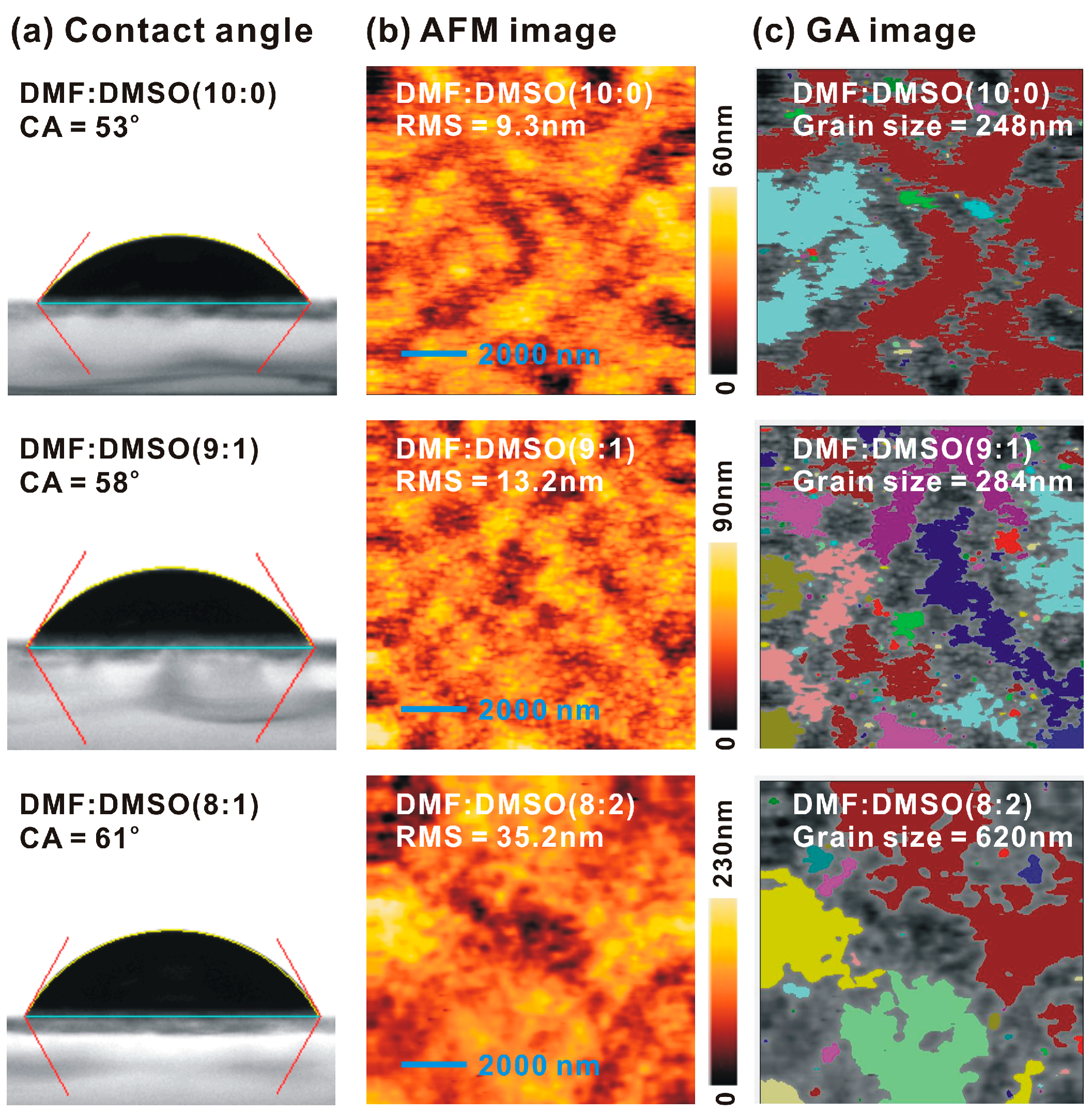
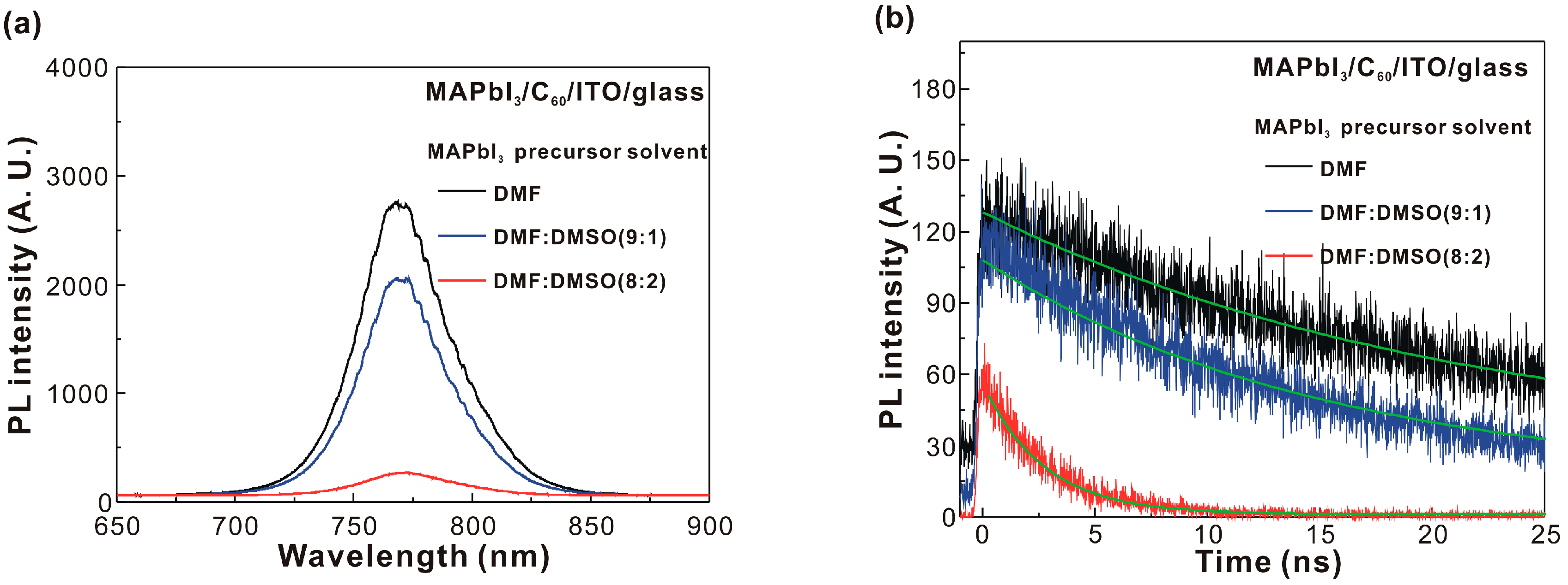
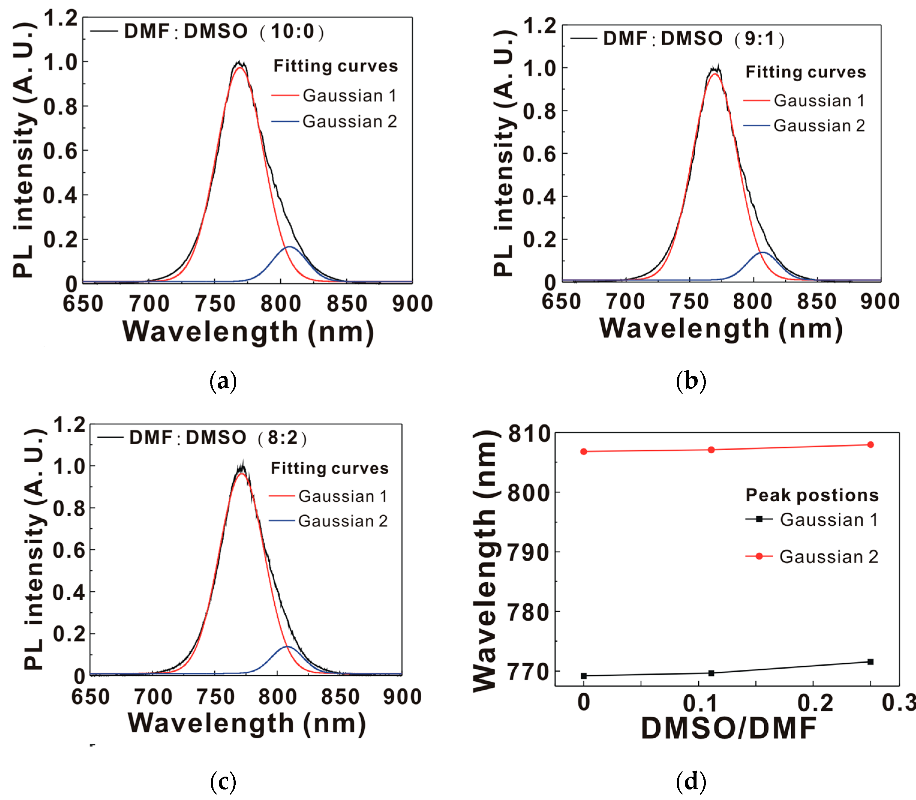
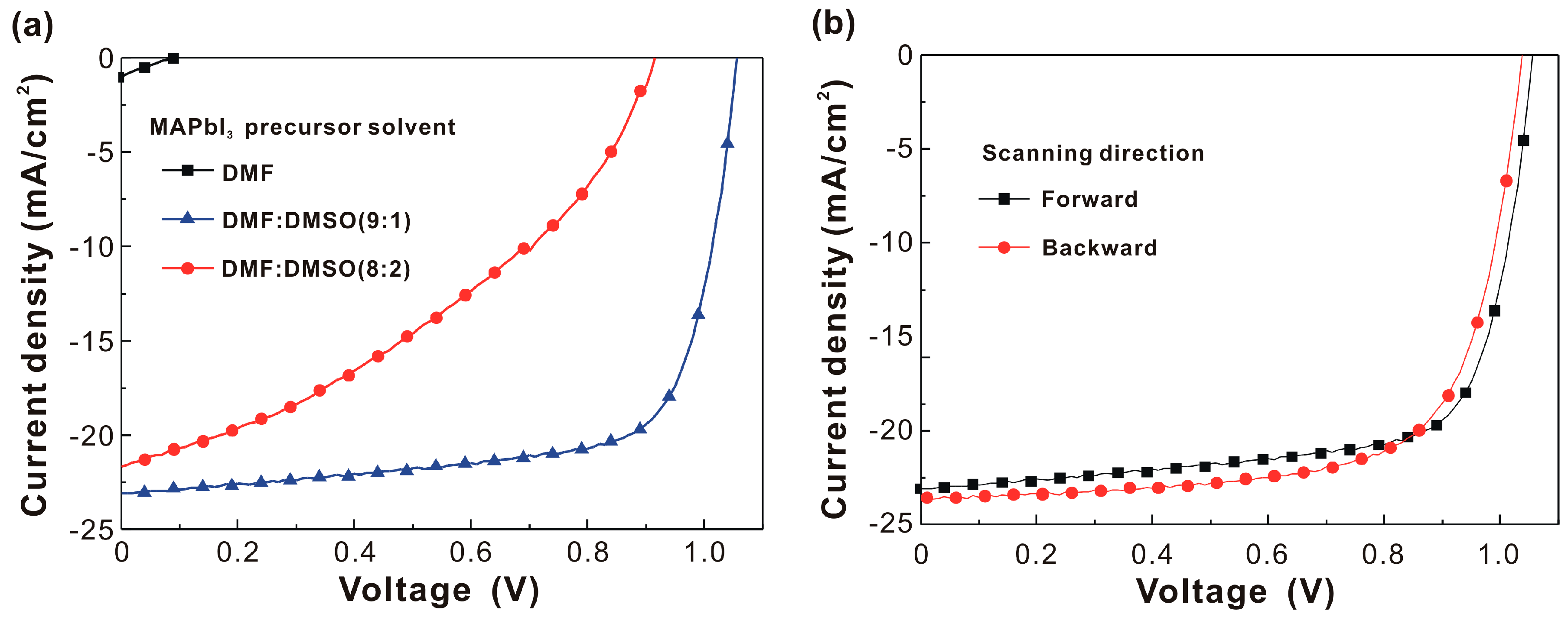
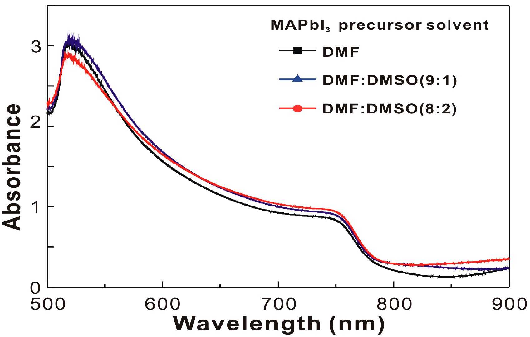
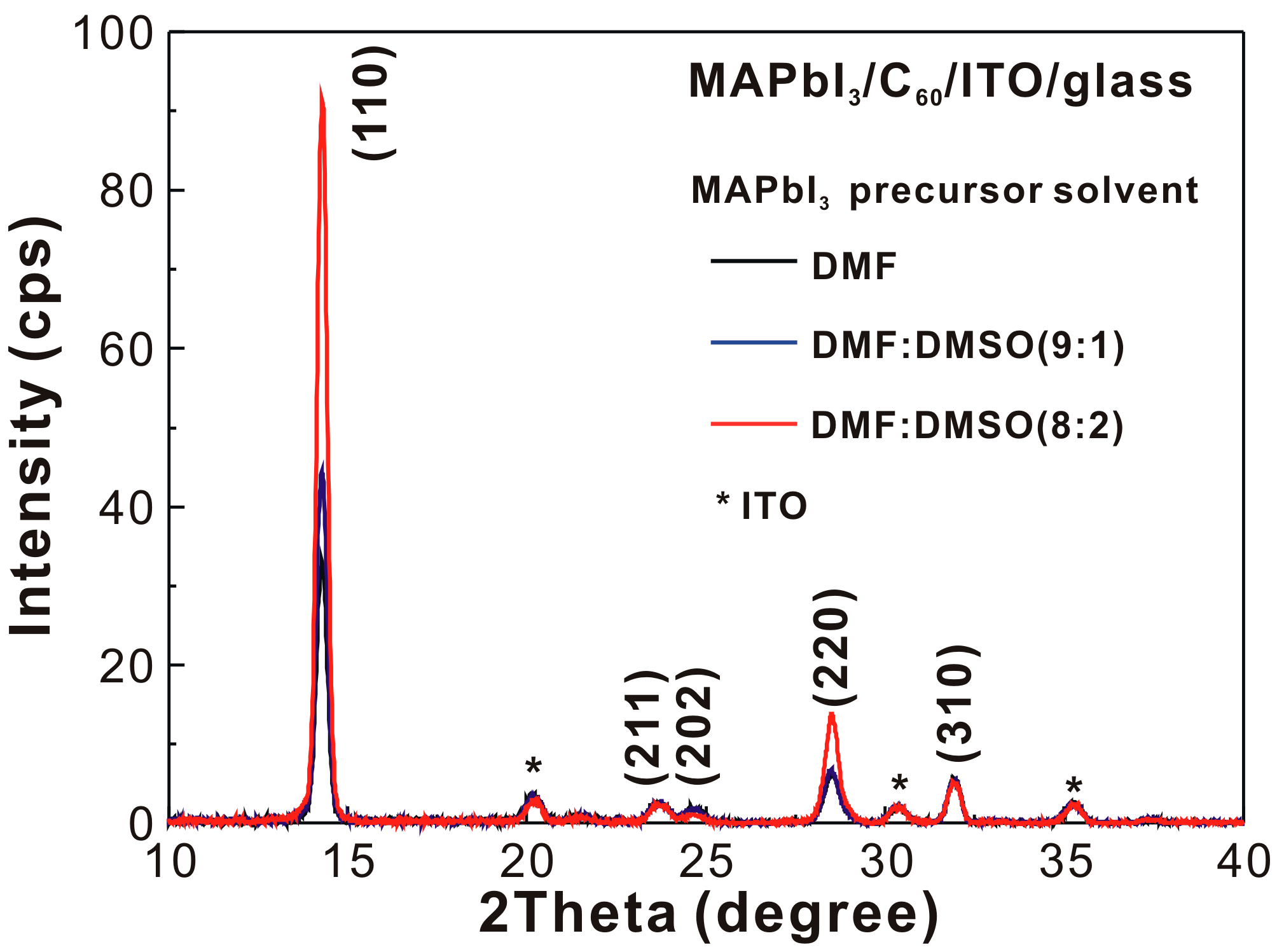
3. Results and Discussion

The J-V curves under a forward scanning direction for the MAPbI3-based solar cells are presented in Figure 1a. The average photovoltaic performance of 16 devices for each fabrication condition is summarized in Table 1. With an increase in the volume ratio of DMSO to DMF from 0/10 to 1/9, the averaged open-circuit voltage (VOC), short-circuit current density (JSC), and fill factor (FF) of the MAPbI3-based photovoltaics dramatically increased from 0.108 V, 0.84 mA/cm2, and 22.9% to 1.045 V, 22.10 mA/cm2, and 70.1%, respectively. This implied that the addition of DMSO in the MAPbI3 precursor changed the properties of the resultant MAPbI3 thin films. The averaged FF (PCE) of the MAPbI3-based photovoltaics significantly decreased from 70.1% (16.21%) to 39.2% (7.80%) with an increase in the volume ratio of DMSO to DMF from 1/9 to 2/8. The reduction in the FF from 70.1% to 39.2% was due to the reduced shunt resistance and the increased series resistance, which suggested poor interfacial contacts [31]. To assess the hysteresis effect of MAPbI3-based photovoltaics, the J-V curves were measured under different scanning directions as shown in Figure 1b. The hysteresis in the J-V curves indicated that the PCE could be further increased when the origins of the hysteresis were diminished.
The droplet contact angles on the C60/ITO/glass sample, as presented in Figure 2a, indicate that the addition of DMSO decreased the wettability of the MAPbI3 precursor solutions on the C60 thin film. It has previously been demonstrated that larger contact angles on the substrate resulted in a crystalline perovskite thin film on the substrate due to the non-wetting surface-driven high-aspect-ratio crystalline grain growth [32]. Figure 2b presents the surface morphologies of the MAPbI3/C60/ITO/glass samples. The average grain sizes (see Figure 2c) and peak-to-valley heights of the MAPbI3 thin films were determined by the built-in graphical analysis tools in the AFM measurement system, where the trend of the grain sizes was proportional to the trend of the contact angles. Conceptually, the roughened MAPbI3 thin films with a large peak-to-valley height of 268 nm could not be completely covered with a 125 nm-thick Spiro-OMeTAD thin film. Therefore, the reduction in the FF from 70.1% to 39.2% was due to poor contact at the interface between the MAPbI3 and the Spiro-OMeTAD when the volume ratio of DMSO to DMF increased from 1/9 to 2/8.
Figure 3 presents the absorbance spectra of the MAPbI3/C60/ITO/glass samples. For 250 nm-thick MAPbI3 thin films, the amplitude of the ripple in the wavelength region from 800–900 nm can be used to assess the surface roughness of the MAPbI3 thin film as the amplitude trend of the ripple is inversely proportional to the surface roughness of the MAPbI3 thin film [33]. Furthermore, the addition of DMSO to the MAPbI3 precursor solution did not significantly influence the light harvesting ability in the resultant MAPbI3 thin films.
Figure 4 presents the X-ray diffraction patterns of the MAPbI3/C60/ITO/glass samples. The main diffraction peak (110) was used to calculate the crystal domain sizes of the MAPbI3 thin films with the Scherrer equation, which are listed in Table 2. Results indicated that the addition of DMSO in the MAPbI3 precursor solution did increase the crystallinity of the resultant MAPbI3 thin films.
Figure 5a presents the PL spectra of MAPbI3/C60/ITO/glass samples. When the hot excitons relax to the conduction band from the excited state through rapid thermalization (downhill relaxation), about half of the excitons in the MAPbI3 thin film can self-dissociate at room temperature and form free carriers, due to the low exciton binding energies [6,7,8,9]. As the other half of the excitons have to diffuse to the p-n junction interface to generate free carriers, the PL intensity from the residual excitons in the MAPbI3 thin films can be used to evaluate the exciton dissociation at the interface. The addition of DMSO in the MAPbI3 precursor solution decreased the PL intensity of the MAPbI3 thin film, indicating that the PL quenching ability was proportional to the crystallinity of the MAPbI3 thin film. Figure 5b presents the exciton dynamics in the MAPbI3/C60/ITO/glass samples. The time-dependent PL intensity was fitted with an exponential decaying function to obtain the exciton lifetime (see Table 2) in the MAPbI3 thin film. The trend of the exciton lifetimes was consistent with the trend of the PL intensities, which indicated that PL quenching was due to exciton dissociation at the interface between the MAPbI3 thin film and C60 thin film. The decreased PL intensity and PL lifetime were not caused by the trap-assisted nonradiative recombination as the exciton lifetimes (or PL lifetimes) of the MAPbI3 thin films on C60/ITO/glass were shorter than the time (~100 ns) for the electrons to transfer from the conduction band to the trap level in the MAPbI3 thin films [34]. The addition of DMSO increased the exciton dissociation rate at the interface between the MAPbI3 and C60 thin films. To analyze the asymmetric characteristics in the PL spectrum, the normalized PL spectrum was fitted with the two Gaussian curves shown in Figure 6. There were two Gaussian peaks at the wavelengths of ~770 nm and ~807 nm, which were assigned to the radiative decays from the band-to-band transition and the trap-assisted transition of the MAPbI3 thin film [35], respectively. The fitting results indicated that the emission wavelengths of the two Gaussian peaks were both red-shifted when the addition of DMSO in the MAPbI3 precursor solution was increased. The peak emission wavelengths of the MAPbI3/C60/ITO/glass samples are listed in Table 2. The trend of the peak emission wavelengths was proportional to the trend of the crystal domain sizes of the MAPbI3 thin films. The intensity ratio of Gaussian 1 to Gaussian 2 (see Table 2) was used to assess the crystallinity of the corresponding MAPbI3 thin film. In addition, the trend of the peak positions of Gaussian 1 was proportional to the crystal domain sizes of the MAPbI3 thin films.
To deposit a hydrophilic MAPbI3 thin film on top of a hydrophobic C60 thin film, DMF was used as the solvent to increase the wetting force of the MAPbI3 precursor solution on C60 thin film, as shown in Figure 1a. The addition of DMSO to the MAPbI3 precursor solution increased the crystallinity of the MAPbI3 thin film, or in other words, the wettability of the DMF on the C60 thin film and the high boiling point of the DMSO (189 °C) increased the nucleation and crystal growth of the MAPbI3 thin film, respectively. Therefore, there was a trade-off between the thin-film continuity and crystallinity for the formation of a MAPbI3 thin film. The high VOC (1.045 V) was the result of the difference between the Fermi level of the Spiro-OMeTAD thin film, and the Fermi level of the C60 thin film. The high JSC (22.1 mA/cm2) was due to the large light-harvesting ability of the multi-crystalline MAPbI3 thin film. The high FF (70.1%) was explained as being due to the formation of a smooth crystalline MAPbI3 thin film, which was advantageous to the smooth contact between the MAPbI3 thin film and the Spiro-OMeTAD capping layer.

4. Conclusions

In summary, we fabricated a high performance C60-based CH3NH3PbI3 (MAPbI3) photovoltaic cell. The highest power conversion efficiency (PCE) was 17.55% (17.20%) under the forward (backward) scanning direction under one sun illumination. The high PCE relied on the formation of a smooth crystalline hydrophilic MAPbI3 thin film on a hydrophobic C60 thin film. By increasing the amount of DMSO added to the MAPbI3 precursor solution, the crystallinity and peak-to-valley height of the MAPbI3 thin film was increased. This occurred as a result of the increase in crystal growth time and a reduction in the number of nucleation sites, which resulted in an optimized photovoltaic performance when the volume ratio of DMSO to DMF was 1/9. The experimental results (atomic-force microscopic images and x-ray diffraction patterns) indicated that the 305-nm MAPbI3 grain was a multi-crystalline MAPbI3 particle with a crystal domain size of ~23 nm. Thus, it was possible to increase the PCE by increasing the crystallinity of the MAPbI3 thin film while keeping a low surface roughness.

Acknowledgments

This work was supported by the Ministry of Science and Technology under Grant MOST 105-2221-E-027-055.

Author Contributions

Lung-Chien Chen wrote the paper, designed the experiments, and analyzed the data. Yu-Shiang Lin, Zong-Liang Tseng, Chiale Wu, and Feng-Sheng Kao prepared the samples and performed all measurements. Sheng-Hui Chen designed the experiments and discussed the results. All authors read and approved the final manuscript.

Conflicts of Interest

The authors declare no conflict of interest.

References

  1. Burschka, J.; Pellet, N.; Moon, S.J.; Humphry-Baker, R.; Gao, P.; Nazeeruddin, M.K.; Grätzel, M. Sequential deposition as a route to high-performance perovskite-sensitized solar cells. Nature 2013, 499, 316–319. [Google Scholar] [CrossRef] [PubMed]
  2. Chiang, C.H.; Tseng, Z.L.; Wu, C.G. Planar heterojunction perovskite/PC71BM solar cells with enhanced open-circuit voltage via a (2/1)-step spin-coating process. J. Mater. Chem. A 2014, 2, 15897–15903. [Google Scholar] [CrossRef]
  3. Jeon, N.J.; Noh, J.H.; Kim, Y.C.; Yang, W.S.; Ryu, S.; Seok, S.I. Solvent engineering for high-performance inorganic-organic hybrid perovskite solar cells. Nat. Mater. 2014, 13, 897–903. [Google Scholar] [CrossRef] [PubMed]
  4. Xiao, M.; Huang, F.; Huang, W.; Dkhissi, Y.; Zhu, Y.; Etherigde, J.; Gray-Weale, A.; Bach, U.; Cheng, Y.B.; Spiccia, L. A fast deposition-crystallization procedure for highly efficient lead iodide perovskite thin-film solar cells. Angew. Chem. 2014, 126, 10056–10061. [Google Scholar] [CrossRef]
  5. Wolf, S.D.; Holovsky, J.; Moon, S.J.; Loper, P.; Niesen, B.; Ledinsky, M.; Haug, F.J.; Yum, J.H.; Ballif, C. Organometallic halide perovskites: Sharp optical absorption edge and its relation to photovoltaic performance. J. Phys. Chem. Lett. 2014, 5, 1035–1039. [Google Scholar] [CrossRef] [PubMed]
  6. Tanaka, K.; Kondo, T. Bandgap and exciton binding energies in lead-iodide-based natural quantum-well crystals. Sci. Technol. Adv. Mater. 2003, 4, 599–604. [Google Scholar] [CrossRef]
  7. Lin, Q.; Armin, A.; Nagiri, R.C.R.; Burn, P.L.; Meredith, P. Electro-optics of perovskite solar cells. Nat. Photonics 2015, 9, 106–112. [Google Scholar] [CrossRef]
  8. Yang, Y.; Ostrowski, D.P.; France, R.M.; Zhu, K.; Lagemaat, J.; van de Lagemaat, J.; Luther, J.M.; Beard, M.C. Observation of a hot-phonon bottleneck in lead-iodide perovskites. Nat. Photonics 2016, 10, 53–59. [Google Scholar] [CrossRef]
  9. Chen, C.C.; Chang, S.H.; Chen, L.C.; Tsai, C.L.; Cheng, H.M.; Huang, W.C.; Chen, W.N.; Lu, Y.C.; Tseng, Z.L.; Chiu, K.Y.; et al. Interplay between nucleation and crystal growth during the formation of CH3NH3PbI3 thin films and their application in solar cells. Sol. Energy Mater. Sol. Cells 2017, 159, 583–589. [Google Scholar] [CrossRef]
  10. Stranks, S.D.; Burlakov, V.M.; Leijtens, T.; Ball, J.M.; Goriely, A.; Snaith, H.J. Recombination kinetics in organic-inorganic perovskites excitations, free charge, and subgap states. Phys. Rev. Appl. 2014, 2, 034007. [Google Scholar] [CrossRef]
  11. Jiang, Y.; Wen, X.; Benda, A.; Sheng, R.; Ho-Baillie, A.W.Y.; Huang, S.; Huang, F.; Cheng, Y.B.; Green, M.A. Time-resolved fluorescence anisotropy study of organic lead halide perovskite. Sol. Energy Mater. Sol. Cells 2016, 151, 102–112. [Google Scholar] [CrossRef]
  12. Chen, C.C.; Chang, S.H.; Chen, L.C.; Kao, F.S.; Cheng, H.M.; Yeh, S.C.; Chen, C.T.; Wu, W.T.; Tseng, Z.L.; Chuang, C.L.; et al. Improving the efficiency of inverted mixed-organic-cation perovskite absorber based photovoltaics by tailing the surface roughness of PEDOT:PSS thin film. Sol. Energy 2016, 134, 445–451. [Google Scholar] [CrossRef]
  13. Zhao, T.; Shi, W.; Xi, J.; Wang, D.; Shuai, Z. Intrinsic and extrinsic charge transport in CH3NH3PbI3 perovskites predicted from first-principles. Sci. Rep. 2016, 6, 19968. [Google Scholar] [CrossRef] [PubMed]
  14. Chang, S.H.; Lin, K.-F.; Cheng, H.-M.; Chen, C.-C.; Wu, W.-T.; Chen, W.-N.; Wu, P.-J.; Chen, S.-H.; Wu, C.-G. Influence of organic cations on high-performance CH3NH3PbI3 based photovoltaics. Sol. Energy Mater. Sol. Cells 2016, 145, 375–381. [Google Scholar] [CrossRef]
  15. Guo, Z.; Manser, J.S.; Wan, Y.; Kamat, P.V.; Huang, L. Spatial and temporal imaging of long-range charge transport in perovskite thin films by ultrafast microscopy. Nat. Commun. 2015, 6, 7471. [Google Scholar] [CrossRef] [PubMed]
  16. Milot, R.L.; Eperon, G.E.; Snaith, H.J.; Johnston, M.B.; Herz, L.M. Temperature-dependent charge-carrier dynamics in CH3NH3PbI3 perovskite thin films. Adv. Funct. Mater. 2015, 25, 6218–6227. [Google Scholar] [CrossRef]
  17. Wang, J.L.H.; Li, H.; Zuo, C.; Wang, H. Thermal stability and optimal photoinduced hydrophilicity of mesoporous TiO2 thin films. J. Phys. Chem. C 2012, 116, 9517–9525. [Google Scholar] [CrossRef]
  18. Kojima, A.; Teshima, K.; Shirai, Y.; Miyasaka, T. Organometal halide perovskite as visible-light sensitizers for photovoltaic cells. J. Am. Chem. Soc. 2009, 131, 6050–6051. [Google Scholar] [CrossRef] [PubMed]
  19. Zhou, H.; Chen, Q.; Li, G.; Luo, S.; Song, T.-B.; Duan, H.-S.; Hong, Z.; You, J.; Liu, Y.; Yang, Y. Interface engineering of highly efficient perovskite solar cells. Science 2014, 345, 542–546. [Google Scholar] [CrossRef] [PubMed]
  20. Jeng, J.-Y.; Chiang, Y.-F.; Lee, M.-H.; Peng, S.-R.; Guo, T.-F.; Chen, P.; Wen, T.-C. CH3NH3PbI3 perovskite/fullerene planar-heterojunction hybrid solar cells. Adv. Mater. 2013, 25, 3727–3732. [Google Scholar] [CrossRef] [PubMed]
  21. National Renewable Energy Laboratory (NREL) Best Research-Cell Efficiency Char. Available online: http://www.nrel.gov/ncpv/images/efficiency_chart.jpg (accessed on 29 June 2016).
  22. Rao, H.; Ye, S.; Sun, W.; Yan, W.; Li, Y.; Peng, H.; Liu, Z.; Bian, Z.; Li, Y.; Huang, C. A 19% efficiency achieved in CuOx-based inverted CH3NH3PbIx−3Clx solar cells by an effective Cl doping method. Nano Energy 2016, 27, 51–57. [Google Scholar] [CrossRef]
  23. Bi, C.; Shao, Y.; Yuan, Y.; Xiao, Z.; Wang, C.; Gao, Y.; Huang, J. Understanding the formation and evolution of interdiffusion grown organolead halide perovskite thin films by thermal annealing. J. Mater. Chem. A 2014, 2, 18508–18514. [Google Scholar] [CrossRef]
  24. You, J.; Yang, Y.; Hong, Z.; Song, T.-B.; Meng, L.; Liu, Y.; Jiang, C.; Zhou, H.; Chang, W.-H.; Li, G.; et al. Moisture assisted perovskite film growth for high performance solar cells. Appl. Phys. Lett. 2014, 105, 183902. [Google Scholar] [CrossRef]
  25. Lin, K.-F.; Chang, S.H.; Wang, K.-H.; Cheng, H.-M.; Chiu, K.Y.; Lee, K.-M.; Chen, S.-H.; Wu, C.-G. Unraveling the high performance of tri-iodide perovskite absorber based photovoltaics with a non-polar solvent washing treatment. Sol. Energy Mater. Sol. Cells 2015, 141, 309–314. [Google Scholar] [CrossRef]
  26. Ahn, N.; Son, D.-Y.; Jang, I.-H.; Kang, S.M.; Choi, M.; Park, N.-G. Highly reproducible perovskite solar cells with average efficiency of 18.3% and best efficiency of 19.7% fabricated via lewis based adduct of lead(II) iodide. J. Am. Chem. Soc. 2015, 137, 8696–8699. [Google Scholar] [CrossRef] [PubMed]
  27. Cai, B.; Zhang, W.-H.; Qu, J. Solvent engineering of spin-coating solutions for planar-structured high-efficiency perovskite solar cells. Chin. J. Catal. 2015, 36, 1183–1190. [Google Scholar] [CrossRef]
  28. Cohen, B.-E.; Etgar, L. Parameters that control and influence the organo-metal halide perovskite crystallization and morphology. Front. Optoelectron. 2016, 9, 44–52. [Google Scholar] [CrossRef]
  29. Yoon, H.; Kang, M.S.; Lee, J.-K.; Choi, M. Hysteresis-free low-temperature-processed planar perovskite solar cells with 19.1% efficiency. Energy Environ. Sci. 2016, 9, 2262–2266. [Google Scholar] [CrossRef]
  30. Liu, J.; Wu, Y.; Qin, C.; Yang, X.; Yasuda, T.; Islam, A.; Zhang, K.; Peng, W.; Chen, W.; Han, L. A dopant-free hole-transporting material for efficient and stable perovskite solar cells. Energy Environ. Sci. 2014, 7, 2963–2967. [Google Scholar] [CrossRef]
  31. Hau, S.K.; Yip, H.-L.; Acton, O.; Baek, N.S.; Ma, H.; Jen, A.K.-Y. Interfacial modification to improve inverted polymer solar cells. J. Mater. Chem. 2008, 18, 5113–5119. [Google Scholar] [CrossRef]
  32. Bi, C.; Wang, Q.; Shao, Y.; Yuan, Y.; Xiao, Z.; Huang, J. Non-wetting surface-driven high-aspect-ratio crystalline grain growth for efficient hybrid perovskite solar cells. Nat. Commun. 2015, 6, 7747. [Google Scholar] [CrossRef] [PubMed]
  33. Tikhonravov, A.V.; Trubetskov, M.K.; Tikhonravov, A.A.; Duparre, A. Effects of interface roughness on the spectral properties of thin films and multilayers. Appl. Opt. 2003, 42, 5140–5148. [Google Scholar] [CrossRef] [PubMed]
  34. Leijtens, T.; Eperon, G.E.; Barker, A.J.; Grancini, G.; Zhang, W.; Ball, J.M.; Kandada, A.R.S.; Snaith, H.J.; Petrozza, A. Carrier trapping and recombination: The role of defect physics in enhancing the open circuit voltage of metal halide perovskite solar cells. Energy Environ. Sci. 2016, 9, 3472–3481. [Google Scholar] [CrossRef]
  35. Shao, Y.; Xiao, Z.; Bi, C.; Yuan, Y.; Huang, J. Origin and elimination of photocurrent hysteresis by fullerene passivation in CH3NH3PbI3 planar heterojunction solar cells. Nat. Commun. 2014, 5, 5784. [Google Scholar] [CrossRef] [PubMed]
Figure 1. (a) J-V curves of MAPbI3-based photovoltaics under one sun illumination under forward scanning direction; (b) J-V curves of the best MAPbI3-based photovoltaics under one sun illumination under forward and backward scanning directions.
Nanomaterials 07 00166 g001
Figure 2. (a) Contact angles (CAs) of MAPbI3 precursor solutions on C60/ITO/glass samples; (b) Atomic force microscope (AFM) images of the MAPbI3/C60/ITO/glass samples; (c) Graphical analysis (GA) images of the corresponding AMF images. The standard deviations of the contact angles were smaller than 1°.
Nanomaterials 07 00166 g002
Figure 3. Absorbance spectra of MAPbI3/C60/ITO/glass samples.
Nanomaterials 07 00166 g003
Figure 4. X-ray diffraction patterns of MAPbI3/C60/ITO/glass samples.
Nanomaterials 07 00166 g004
Figure 5. (a) Static photoluminescence spectra of MAPbI3 thin films on C60/ITO/glass; and (b) Nanosecond time-resolved photoluminescence of MAPbI3 thin films on C60/ITO/glass.
Nanomaterials 07 00166 g005
Figure 6. (ac) The normalized PL spectra of the MAPbI3/C60/ITO/glass samples; (d) the peak emission wavelengths of the MAPbI3/C60/ITO/glass samples.
Nanomaterials 07 00166 g006
Table 1. Photovoltaic performance under one sun illumination (AM 1.5G, 100 mW/cm2).
MAPbI3 Precursor SolventVOC (V)JSC (mA/cm2)FF (%)PCE (%)
DMF0.106 ± 0.0280.84 ± 0.6422.9 ± 0.50.02 ± 0.01
DMF:DMSO (9:1)1.045 ± 0.01122.10 ± 1.1770.1 ± 3.216.21 ± 1.29
DMF:DMSO (9:1) a1.05623.1171.917.55
DMF:DMSO (9:1) b1.04023.6969.617.20
DMF:DMSO (8:2)0.929 ± 0.03221.58 ± 0.8839.2 ± 5.27.80 ± 1.40
a Photovoltaic performance of the best cell under the forward scanning direction; b Photovoltaic performance of the best cell under the backward scanning direction.
Table 2. Structural, optical, and excitonic properties of MAPbI3 thin films. PVH: peak-to-valley height; D: crystal domain size; IXRD: peak intensity of XRD at (110); PG1: peak position of Gaussian 1; PG2: peak position of Gaussian 2; Ratio: intensity ratio of Gaussian 1 to Gaussian 2; τ: exciton lifetime of MAPbI3 thin film on C60/ITO/glass sample.
MAPbI3 Precursor SolventPVH (nm)D (nm)IXRDPG1 (nm)PG2 (nm)Ratioτ (ns)
DMF6822.333769.2806.88.4721.55
DMF:DMSO (9:1)14422.744769.6807.110.7115.13
DMF:DMSO (8:2)26824.091771.6808.010.762.71

