Tunable Electronic and Topological Properties of Germanene by Functional Group Modification

School of Physics, University of Jinan, Jinan 250022, China
*
Author to whom correspondence should be addressed.
Nanomaterials 2018, 8(3), 145; https://doi.org/10.3390/nano8030145
Submission received: 5 January 2018
/
Revised: 2 March 2018
/
Accepted: 2 March 2018
/
Published: 6 March 2018
Abstract
:Electronic and topological properties of two-dimensional germanene modified by functional group X (X = H, F, OH, CH3) at full coverage are studied with first-principles calculation. Without considering the effect of spin-orbit coupling (SOC), all functionalized configurations become semiconductors, removing the Dirac cone at K point in pristine germanene. We also find that their band gaps can be especially well tuned by an external strain. When the SOC is switched on, GeX (X = H, CH3) is a normal insulator and strain leads to a phase transition to a topological insulator (TI) phase. However, GeX (X = F, OH) becomes a TI with a large gap of 0.19 eV for X = F and 0.24 eV for X = OH, even without external strains. More interestingly, when all these functionalized monolayers form a bilayer structure, semiconductor-metal states are observed. All these results suggest a possible route of modulating the electronic properties of germanene and promote applications in nanoelectronics.
1. Introduction
Due to the novel electronic properties, graphene has attracted plenty of interest since its discovery [1,2,3,4,5], including massless Dirac fermion, high thermal conductivity, and high carrier mobility (200,000 cm2/(v s)) [6,7]. Flexibility of graphene is also essential for flexible nanoelectronics, which has produced a lot of products in experiments [8,9,10]. It has a thermal conductivity of 5000 Wm−1 K−1 at room temperature, offering an advantage for membrane technology [11]. The ambient stability favors sustainable exploitation in nanoelectronics [12]. Moreover, it has half-integer Hall conductance, which indicates promising applications in nanoelectronics. Graphene is also proposed to be a topological insulator (TI) with a band gap opening at the Dirac point by strain or functional group modification with spin-orbit coupling (SOC) [13,14,15]. However, the gap is too small to be detected, let alone having applications at room temperature. In fact, only two-dimensional (2D) TI systems (HgTe/CdTe and InAs/GaSb quantum wells) have been verified in experiments [16,17,18,19]. The prediction and measurement of more 2D TI materials, especially those with large band gaps, is still challenging. These difficulties promote the study of tuning the electronic properties of graphene [20,21]; geometric or chemical modifications are two widely used methods. It also encourages great efforts regarding the search for other honeycomb films composed of heavier group–IV elements such as silicon (Si), germanene (Ge), stanene (Sn) and plumbene (Pb) [22,23,24,25,26,27,28], as well as other group-V films.
Germanene is a promising counterpart of a graphene monolayer, which is a honeycomb monolayer of Ge atoms with a low-buckled (0.84 Å) structure resulted from the weak π-π interaction and distinct coupling of σ and π bonds between Ge atoms [29,30,31,32]. The strength of SOC in germanene is much larger than that in graphene, which leads to a larger band gap at K point, and therefore the expected TI phase may be accessible in experiments. Several remarkable features of germanene have been revealed [28,33,34]. Bianco et al. [35] have synthesized millimeter-scale crystals of hydrogen-terminated germanene from the topochemical deintercalation of CaGe2 compound. Zhang et al. [36,37] have investigated the structural and electronic properties of germanene/germanene heterostructures (HTSs). Germanene on MoS2 has also been proposed, which is a P-doped semiconductor with a band gap of 24 meV [38].
In the present work, we investigate electronic structures and topological properties of chemically functionalized germanene, GeX (X = H, F, CH3, OH), via the use of density functional theory (DFT) calculations. We mainly focus on the effect of both strain and SOC on the band structure. Without considering the effect of SOC, we find that chemical modification will remove the Dirac point at Fermi level and open a direct band gap at Γ point, and which may be well tuned by external strain. Particularly, semiconductor-semimetal phase transition occurs in GeH with increasing strain. Besides this, we also study the bilayer of functionalized germanene, where it can be found that, compared to the band gaps of the isolated germanene monolayer, the band gaps of bilayer are reduced. Functionalization of germanene is a powerful method to produce stable 2D germanene and our results would help to promote the application of germanene in nanoelectronics.
2. Methods
All calculations are performed using the density functional theory (DFT) [39] method as implemented in the Vienna Ab initio Simulation Pack (VASP) code [39,40]. The generalized gradient approximation (GGA) with the Perdew–Burke–Ernzerhot (PBE) are used to describe the exchange-correlation energy [41,42], which is developed for the calculations of surface systems. The projector-augmented wave (PAW) method was used to describe electron–ion potential [43]. The DFT-D2 methods were used throughout all the calculation to properly take into account the van der Waals (vdW) interaction in the bilayer structures [44]. The energy cutoff of the plane-wave is set to be 500 eV with an energy precision of 10−6 eV. A vacuum region of 20 Å was used for the isolated sheet to eliminate any artificial interaction between neighboring super-cells. The Brillouin zone is sampled by using a 9 × 9 × 1 Gamma-centered Monkhorst–Pack (MP) [45] grid. In addition, by using the conjugate gradient method, all atomic positions and the size of the unit cell are optimized until the atomic forces are less than 0.01 eV Å−1. SOC is included by a second vibrational procedure on a fully self-consistent basis. A Wannier90 package with the maximally Localized Wannier functions is used to calculate the topological edge state [46].
3. Results and Discussion
3.1. Monolayer Germanene
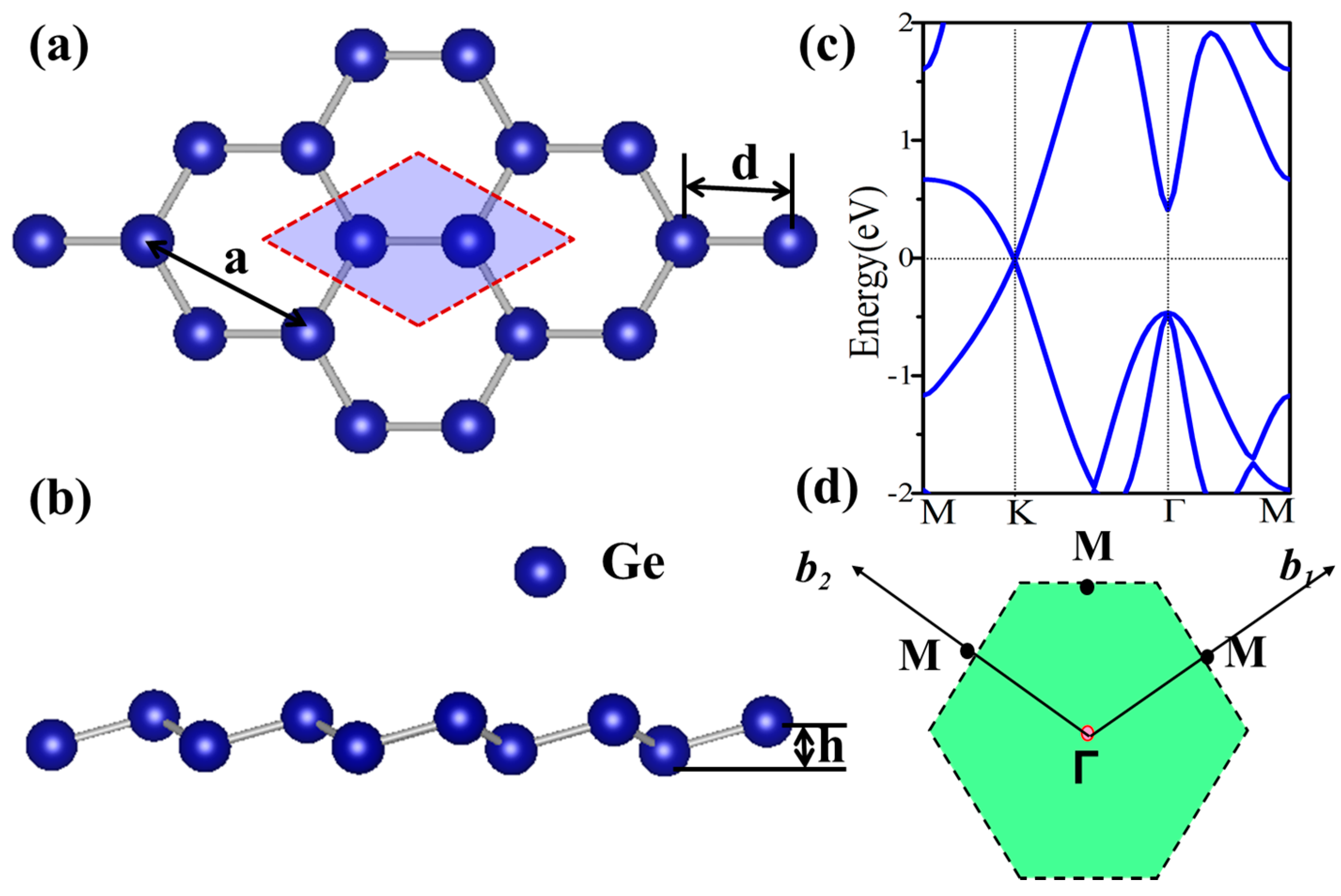
Before studying the functionalized germanene, we first present the geometric and electronic structures of the pristine germanene monolayer, as shown in Figure 1. Germanene has a hexagonal honeycomb structure, and the relaxed lattice parameter is found to be a = 4.06 Å and d = 2.44 Å. It indicates a weaker π-bonding between Ge atoms, resulting in a low-buckled structure (h = 0.69 Å) [47]. The band structure is plotted in Figure 1c, and it is clear that there is a Dirac point at K point near the Fermi level, suggesting a gapless semiconductor. At Γ point, there is a direct gap about 0.86 eV with a two-fold degenerate energy below the Fermi energy, which is mainly attributed to the pxy orbital. The Dirac point is mainly due to the pz orbital, which has a low hybridization with other orbitals. The linear dispersion leads to a high mobility which is important in electronics. To inherit the technology of conventional semiconductor, the opening of a band gap without changing the mobility greatly is expected.
3.2. Functionalized Monolayer Germanene
Functionalization is a widely used method to tune the electronic properties of 2D film materials. In this work, four four-type functional groups (–H, –F, –OH, –CH3) are used. It allows us to design 10 functionalized germanene, four symmetrical (GeX) plotted in Figure 2, and six asymmetrical (X–Ge–X’) ones, as listed in Table 1. Here we denote X–Ge–X’ as the germanene functionalized with radical X on the top side while having radical X’ on the bottom side. We denote GeX as an abbreviation of X–Ge–X’. The structure parameters, formation energies and band gaps are also listed in Table 1. The formation energy is calculated with the formula below.
where E(GeX), E(Ge), and E(X) are energies of the functional germanene, pristine germanene, and X atoms, respectively, as shown in Table 1. The calculated formation energy Ef is −2.61, −4.25, −3.16 and −4.96 eV/atom for GeH, GeF, GeOH and GeCH3, respectively, indicating no phase separation in these systems. In general, we find that the functionalized germanene has larger structural parameters than the pristine one, which is just as expected since electrons will transfer from Ge to X, which enhances the ion-ion interaction, such as with GeH in Figure 3a.
Figure 2 displays the electronic structure of functional germanene GeX (X = H, F, OH, CH3). Note that there is a direct band gap at Γ point with values in the range of 0.15~0.98 eV, while the Dirac point at K point disappears. This is because a strong σ bond forms between Ge and X as shown in Figure 3a, where charge distribution is plotted. For pristine germanene, the Dirac point is mainly due to the pz orbital, and there is a direct gap at Γ point, mainly due to the pxy orbital. Their σ bond between Ge and X moves the pz orbital away from the Fermi level, and therefore we have a direct gap at Γ point. For GeH, the direct gap at Γ point is 0.98 eV, a little larger than that of the pristine germanene, while the band structure of GeCH3 with a smaller direct gap of 0.78 eV. However, the direct gap is much weakened for GeOH and GeF with gap = 0.15 and 0.21 eV, respectively. The possible reason is that the much-enlarged lattice constants weaken the hopping interaction and therefore result in the band gap between the bonding and anti-bonding state. In this case, the Γ point for the high two valence band is broken in GeF and GeOH; it may lead to the direct gap decrease. In addition, for asymmetrical functionalization germanene monolayer, the band gap is between the corresponding two functionalized structures; such as for OH–Ge–H, the band gap is 0.50 eV, compared with the functionalization structure OH–Ge–OH and H–Ge–H which is 0.21 and 1.06 eV, respectively.
External strain is an effective approach to achieve tunable electronic properties. In Figure 4 we plot the evolution of the band gap for the four-symmetrical functionalized germanene. The strain is described by the change of lattice constant ε = (a − a0)/a0, where a (a0) is the lattice constant with (without) strain. In detail, the GeX (X = H, F, OH, CH3) lattice is expanded uniformly along zigzag and armchair directions in the horizontal plane and relaxed along the c-axis. We find that the band gap can be easily tuned, which may be easily realized experimentally. For GeX, the band gap will decrease to zero and reopen with increased strain, as shown in Figure 4. In addition, we take the example of GeH shown in Figure 5. We plot the band structure of GeH under strain 0%, 8% and 9% and find the gap stays closed for strains larger than 8%. Obviously, there is a conduction band and two degenerate valence bands at Γ point near the Fermi level beyond the critical strain, which correspond to the 1D and 2D representations of the symmetry group, respectively. Raising strain will lower the 1D level while lifting the two-fold levels as shown in Figure 5d. In this case, these three bands touch and become three-fold degenerate at Γ point: see Figure 5b. Increasing strain further, thetwo2-fold degenerate levels will lie over the one-fold level: see Figure 5c. Considering the number of electrons, the Fermi level will always cross the touching point, which leads to a semimetal phase.
3.3. Topological Properties
In this section, we turn to the effect of SOC on the band structure. We mainly focus on the four-symmetrical functionalized germanene monolayers. Generally, the coexistence of strain and SOC will lead to a topological nontrivial phase in 2D honeycomb lattice, as has been well studied. We investigate the possible topological phase transition by calculating the index Z2, edge state and analyzing the inverted band structure.
For GeH, the effects of SOC will only change the band structure slightly: see Figure 6b. It is an insulator with a direct gap of 0.94 eV, a little smaller than that (0.98 eV) without SOC. An obvious difference is that SOC breaks the degeneracy of the first two valence bands at the Γ point. However, there is no topological phase transition in the process, and it still lies in the normal insulator phase. Detailed orbital analysis indicates that two pxy levels and a single s level lie below and above Fermi level at Γ point respectively, which is in the same sequence as in the case with no SOC.
Then, we apply the external strain and reveal its cooperation effect with SOC. We find that the band gap decreases to zero and reopens with increased strain, as is shown in Figure 4a. In addition, the external strain affects the chemical properties of honeycomb nanosystems, which can take a topological phase transition which has been reported by Putz [14]. Thus, we believe that the behavior of band gaps suggests that there may be a topological phase transition caused under external strain. The electronic energy spectra for 9% are shown in Figure 6c. One can see that the orbital sequence at Γ point changes from the original s, pxy, pxy to pxy, s, pxy, which leads to an inverted energy band structure and an indirect band gap of 86 meV (a finite band gap of 150 meV opens at Γ) opened under SOC effect. This suggests it is in the TI phase, which is further verified by calculating the topological Z2 index, defined as [48].
Ki is the time reversal invariant momentum in the first Brillouin. For the lattice considered here, there are four time reversal invariant momenta (TRIM) in total, which are Γ (0, 0), M1 (0.5, 0), M2 (0, 0.5), M3 (0.5, 0.5). is the parity of the 2m-th energy level below the Fermi level. In the GeH system, there are 10 valence electrons in a unit cell and therefore N = 5. δ is the product of parity eigenvalues at each TRIM. The Z2 index ν = 0 corresponds to a trivial normal insulator while ν = 1 corresponds to a topological insulator. In Figure 6d, we show the parity of the occupied eigenstate at each TRIM in the case with strain ε = 9%. The Z2 index is calculated to be 1, proving with the prediction of TI phase.
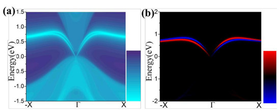
One essential characteristic of 2D TIs is the existence of dissipationless edge states protected by time-reversal symmetry (TRS) [49,50]. The density of state (DOS) of a half infinite monolayer and the corresponding spin polarization as illustrated in Figure 7a,b, respectively. There is a pair of gapless edge states in the gap regime connecting the valence and conduction bands. By identifying the spin distribution, as illustrated in Figure 7b, we find that the counter-propagating edge states have opposite spin-polarizations, as expected for the quantum spin Hall (QSH) phase. The transport due to edge states may be used in the design of quantum electronic devices with low dissipation.
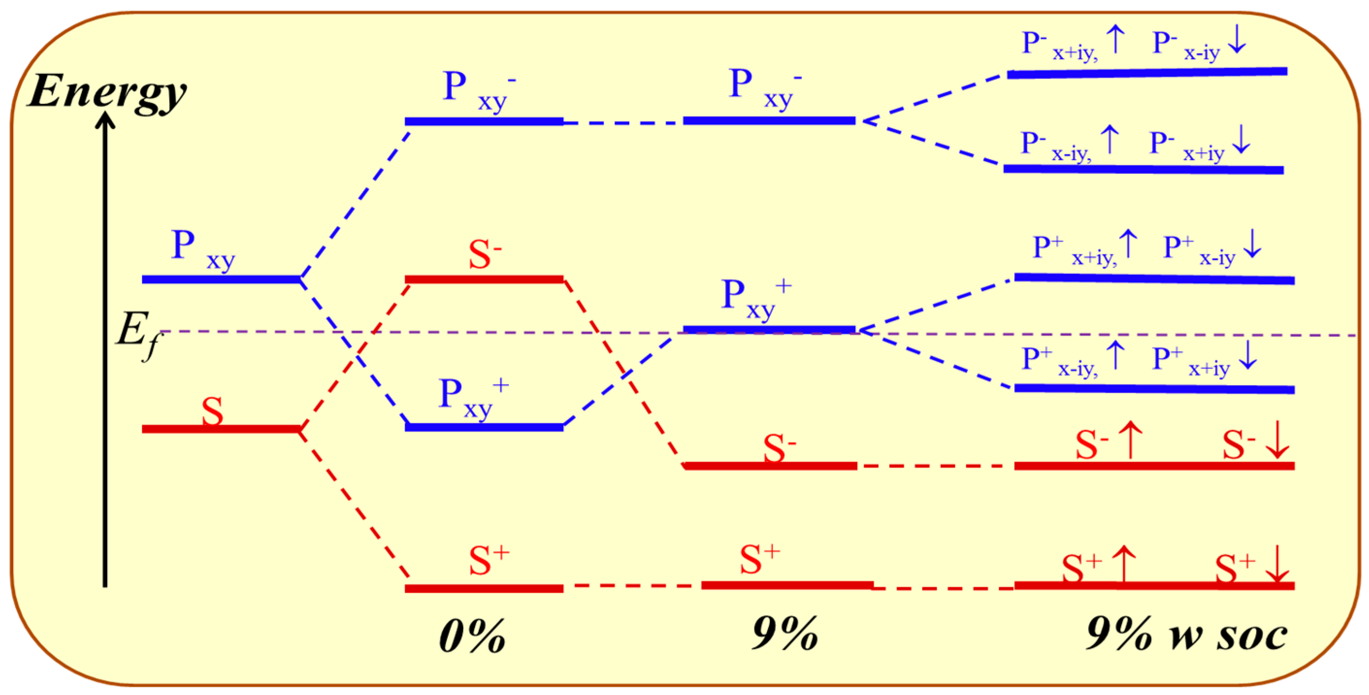
An orbital analysis around Fermi level of GeH is necessary to understand the mechanism of transformation from NI to TI. The corresponding orbital analysis is shown in Figure 8, and the relevant bands are dominated by the Ge-4s and Ge-4pxy states. Due to the chemical bonding between adjacent Ge atoms, these states are split into bonding and anti-bonding states, which the superscripts + and − represent the parities of corresponding states, respectively. Here, where the bands near the Fermi level are contributed by the |s−> and |pxy+> orbital, and the |pxy+> lies below |s−> orbital without an inversion of band order. This is because the larger lattice constant of GeH (4.09 Å) results in a weaker s-p hybridization and is according to a smaller energy separation between the bonding and anti-bonding states. When the in-plane strain is applied to ε = 9%, the band order of GeH monolayer is changed, the |s−> orbital is downshifted while the |pxy+> orbital is upshifted, leading an s-p band inversion around Fermi level. With the inclusion of SOC, the degeneracy of the level splits into |p, ±3/2> state with a total angular momentum j = 1/2, open a band gap. In other words, increasing the lattice constant weakens the interaction between the Ge atoms. This decreases the splitting between the bonding and anti-bonding states, which make signifying that a GeH monolayer with ε = 9% is a QSH insulator.
Furthermore, the topological properties of GeX (X = F, OH, CH3) monolayers are also studied, which shows similar results as GeH. Figure 4 gives the evolution of band gap at Γ point (EΓ) and global band gap (Eg) against external strain in the presence of SOC. As is shown, it is a direct gap insulator on the left of the critical point, while it becomes an indirect gap for a moderate tensile strain which is especially clear for GeOH. As is well known, it is necessary for the band gap to close and reopen to realize the phase transition from the normal insulator to the topological insulator phase. These demonstrate the emergence of topological nontrivial phase. Also, the calculations of Z2 invariants verify a NI (Z2 = 0)—TI (Z2 = 1) transition.
The critical point for the topological phase transition emerges at a positive tensile strain for GeH (a = 4.39Å, ε = 8%) and GeCH3 (a = 4.363 Å, ε = 6%) while it lies at a negative compressive strain for GeF (a = 4.22 Å, ε = −2.8%) and GeOH (a = 4.18 Å, ε = −1.3%). Thus, the external strain is essential for GeCH3 to realize the TI phase while SOC is to open the energy gap, which is identical to the case of GeH. However, TI phase has already formed for GeF and GeOH in the case with no external strain. Particularly, we would point out that the band gap of GeF with no strain is quite large, about 0.19 eV, which is much larger than kBT at room temperature (26 meV), indicating edge states in GeF could be measured at room temperature. A tensile strain can only change the band gap of GeF and GeCH3 slightly. However, strain will greatly change the band gap of GeOH. It becomes as large as 0.71 eV for GeOH with the strain 9%, such large band gap of TI will be essential for potential applications at room temperature.
3.4. Bilayer of Functionalized Germanene
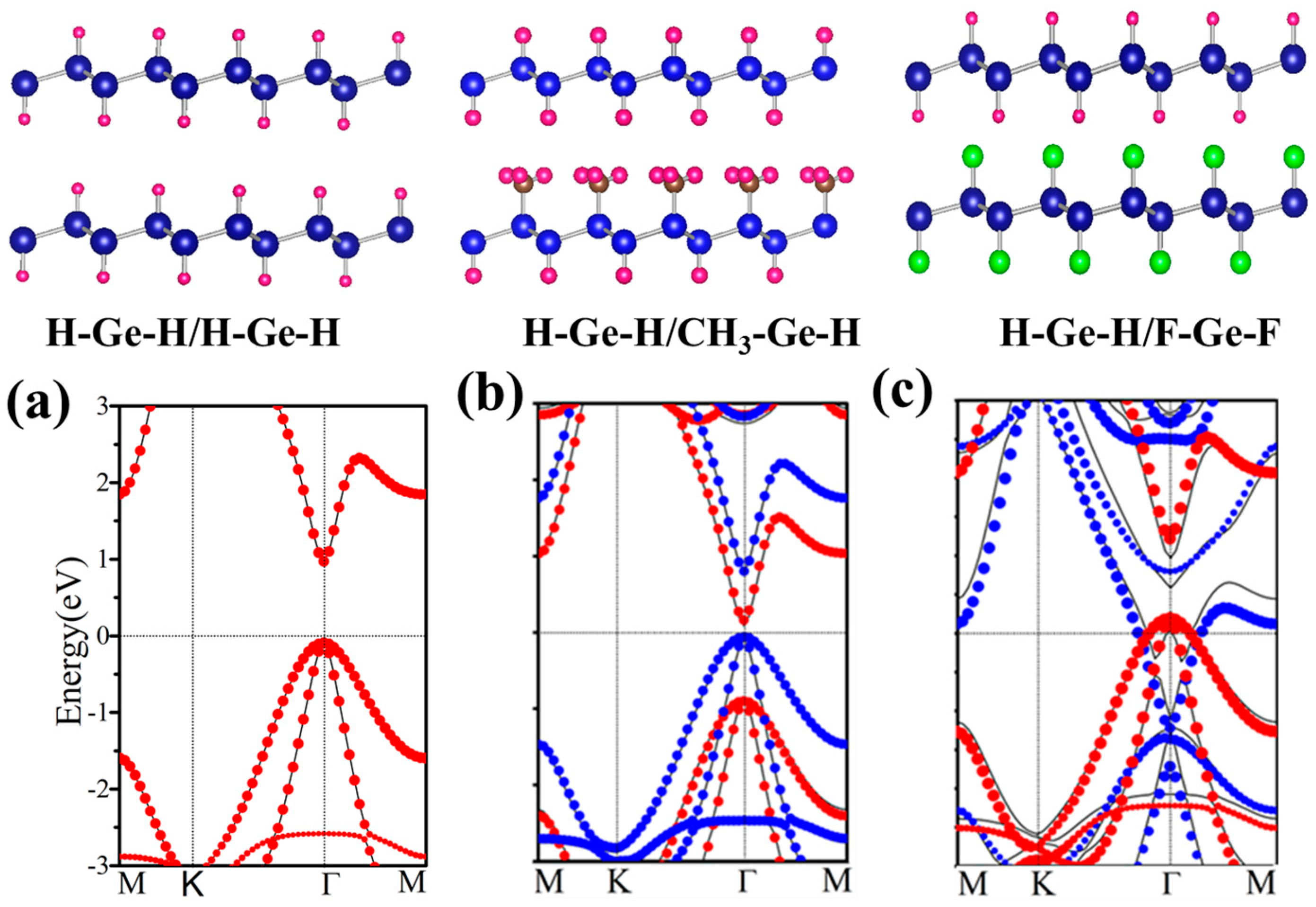
In this section, we construct AA stacked bilayers of functionalized germanene denoted as X–Ge–X’/Y–Ge–Y’ with monolayer X–Ge–X’ on the top of monolayer Y–Ge–Y’. All structures studied are listed in Table 2 with geometry and electronic parameters. Some of which are plotted in Figure 9. It is expected that it would be possible to further control and improve the electronic properties of functionalized germanene by constructing this bilayer structure.
According to the change of structures, all bilayers can be classified into two classes with one functional group or different functional groups decorated germanene, respectively. If the bilayer is composed of two identical monolayers, band gap and the other geometry parameters change only a little. In Figure 9a, the band structure of H–Ge–H/H–Ge–H is plotted, which is nearly the same as that of H–Ge–H. It indicates that it is a Van der Waals interaction rather than chemical bonding formed between these two layers. For another class, there are different functional groups decorated germanene, such as H–Ge–H/CH3–Ge–H, shown in Figure 9b. A direct band gap of 0.18 eV is presented, with its valence band maximum (VBM) and conduction band minimum (CBM) located at Γ point, less than 0.98 and 0.86 eV of H–Ge–H and CH3–Ge–H monolayer.
Further analysis indicates that the wave functions of CBM and VBM are located in the H–Ge–H and CH3–Ge–H layers, respectively. In Figure 9b, we plot energy spectra of H–Ge–H and CH3–Ge–H as red and blue dots, respectively. We find that they fit the energy band of the H–Ge–H/CH3–Ge–H bilayer very well. It suggests that no chemical bonding is formed between two layers, and the energy band is nearly a direct combination of the H–Ge–H and CH3–Ge–H monolayers.
H–Ge–CH3/CH3–Ge–H, H–Ge–F/F–Ge–H et al. also have similar results and these results are all in line with those obtained by Li et al. [51] and Pablo et al. [52]. In addition, the second class has another case, such as H–Ge–H/F–Ge–H, H–Ge–H/F–Ge–F, H–Ge–F/CH3–Ge–H and H–Ge–HO/CH3–Ge-H, where the structure is metal phase. Here, H–Ge–H/F–Ge–F is taken as an example as shown in Figure 9c. It indicates that the Fermi level of one monolayer crosses the energy band of the other monolayer. It means a larger interlayer interaction than in the other structures. To gain further insight into the band gap, we have analyze the plane-integrated electron density differences in Figure 3b. A large charge transfer from H–Ge–H to F–Ge–F monolayer happens, as is expected, consistent with the energy spectra where the original conduction band of F–Ge–F layer lies partly below the Fermi level while the original valence band of the H–Ge–H layer lies partly above the Fermi level. Besides this, we find that the band gap of the bilayer is only slightly changed with the changing of the distance of two component monolayers, which suggests that the interlayer Van der Waals interaction is almost not affected by the change of interlayer distance. Our results show that X–Ge–X’/Y–Ge–Y’ can be conveniently tuned by decorated group, which makes it a promising platform for applications in experiments and electronic devices.
4. Conclusions
Based on first-principles calculations, we studied the electronic properties of germanene modified by functional group X (X = H, F, OH, CH3). In the monolayer case, we find that the functional group will remove the original Dirac point of pristine germanene at K point and open a gap at Γ point, which can be tuned well by external strain. On the other hand, we have predicted a new class of 2D QSH insulators in GeH monolayers by the external strain. For GeH, external strain can change the band gap significantly and lead to a NI–TI phase transition in the presence of SOC. Further analysis based on orbital analysis indicates that the topology mainly stems from s-pxy orbital of Ge atoms, and the strong SOC is only open a band gap. Lastly, we find that bilayer structures (X–Ge–X’/Y–Ge–Y’) can be conveniently tuned by decorated group. These results suggest a possible route to tune the electronic properties of germanene and provide competitive candidates of TIs for potential applications in nanoelectronics at room temperature.
Acknowledgments
This work was supported by the National Natural Science Foundation of China (Grant No. 61571210, 61172028 and 11434006).
Author Contributions
Chang-Wen Zhang and Pei-Ji Wang conceived the idea and designed the calculated model. Ceng-Ceng Ren carried out the electronic structure calculations and data analysis. Shu-Feng Zhang, Wei-Xiao Ji and Ping Li performed the analysis method of the properties. All authors have given approval to the final version of the manuscript.
Conflicts of Interest
The authors declare no conflict of interest.
References
- Novoselov, K.S.; Geim, A.K.; Morozov, S.V.; Jiang, D.; Katsnelson, M.I.; Grigorieva, I.V.; Doubonos, S.V.; Firsov, A.A. Two-Dimensional Gas of Massless Dirac Fermions in Graphene. Nature 2005, 438, 197–200. [Google Scholar] [CrossRef] [PubMed] [Green Version]
- Katsnelson, M.I.; Novoselov, K.S.; Geim, A.K. Klein paradox in graphene. Nat. Phys. 2006, 2, 620–625. [Google Scholar] [CrossRef] [Green Version]
- Tang, Q.; Zhou, Z. Graphene-Analogous Low-Dimensional Materials. Prog. Mater. Sci. 2013, 58, 1244–1315. [Google Scholar] [CrossRef]
- Allen, M.J.; Tung, V.C.; Kaner, R.B. Honeycomb Carbon: A Review of Graphene. Chem. Rev. 2010, 110, 132–145. [Google Scholar] [CrossRef] [PubMed]
- Geim, A.K. Graphene: Status and prospects. Science 2009, 324, 1530–1534. [Google Scholar] [CrossRef] [PubMed]
- Guzmán-Verri, G.G.; Voon, L.C.L.Y. Electronic structure of silicon-based nanostructures. Phys. Rev. B 2011, 76, 12825–12834. [Google Scholar] [CrossRef]
- Novoselov, K.S.; Geim, A.K.; Morozov, S.V.; Jiang, D.; Zhang, Y. Electric Field Effect in Atomically Thin Carbon Films. Science 2004, 306, 666–669. [Google Scholar] [CrossRef] [PubMed]
- Kady, M.; Strong, V.; Dubin, S.; Kaner, R.B. Laser scribing of high-performance and flexible graphene-based. Science 2012, 335, 1326. [Google Scholar] [CrossRef] [PubMed]
- Pei, S.; Zhao, J.; Du, J.; Ren, W.; Cheng, H.M. Direct reduction of graphene oxide films into highly conductive and flexible graphene films by hydrohalic acids. Carbon 2010, 48, 4466–4474. [Google Scholar] [CrossRef]
- Xu, Y.; Bai, H.; Lu, G.; Li, C.; Shi, G. Flexible Graphene Films via the Filtration of Water-Soluble Noncovalent Functionalized Graphene Sheets. J. Am. Chem. Soc. 2008, 130, 5856. [Google Scholar] [CrossRef] [PubMed]
- Gugliuzza, A.; Politano, A.; Drioli, E. The advent of graphene and other two-dimensional materials in membrane science and technology. Curr. Opin. Chem. Eng. 2017, 16, 78–85. [Google Scholar] [CrossRef]
- Politano, A.; Vitiello, M.S.; Viti, L.; Boukhvalov, D.W.; Chiarello, G. The role of surface chemical reactivity in the stability of electronic nanodevices based on two-dimensional materials “beyond graphene” and topological insulators. FlatChem 2016, 1, 60–64. [Google Scholar] [CrossRef]
- Putz, M.V.; Ori, O. Bondonic Characterization of Extended Nanosystems: Application to Graphene’s Nanoribbons. Chem. Phys. Lett. 2012, 548, 95–100. [Google Scholar] [CrossRef]
- Putz, M.V.; Ori, O. Bondonic effects in group-IV honeycomb nanoribbons with Stone-Wales topological defects. Molecules 2014, 19, 4157–4188. [Google Scholar] [CrossRef] [PubMed]
- Putz, M.V.; Ori, O. Predicting bondons by Goldstone mechanism with chemical topological indices. Int. J. Quantum. Chem. 2015, 115, 137–143. [Google Scholar] [CrossRef]
- Bernevig, B.A.; Hughes, T.L.; Zhang, S.C. Quantum Spin Hall Effect and Topological Phase Transition in HgTe Quantum Wells. Science 2006, 314, 1757–1761. [Google Scholar] [CrossRef] [PubMed]
- König, M.; Wiedmann, S.; Brüne, C.; Roth, A.; Buhmann, H.; Molenkamp, L.W.; Qi, X.L.; Zhang, S.C. Quantum Spin Hall Insulator State in HgTe Quantum Wells. Science 2007, 318, 766–770. [Google Scholar] [CrossRef] [PubMed]
- Du, L.; Knez, I.; Sullivan, G.; Du, R.R. Robust Helical Edge Transport in Gated InAs/GaSb Bilayers. Phys. Rev. Lett. 2015, 114, 096802. [Google Scholar] [CrossRef] [PubMed]
- Liu, C.; Hughes, T.L.; Qi, X.L.; Wang, K.; Zhang, S.C. Quantum Spin Hall Effect in Inverted Type-II Semiconductors. Phys. Rev. Lett. 2008, 100, 236601. [Google Scholar] [CrossRef] [PubMed]
- Miller, D.L.; Kubista, K.D.; Rutter, G.M.; Ruan, M.; de Heer, W.A.; First, P.N.; Stroscio, J.A. Structural analysis of multilayer graphene via atomic moiré interferometry. Phys. Rev. B 2010, 81, 125427. [Google Scholar] [CrossRef]
- Zhang, R.; Zhang, C.; Ji, W.; Ren, M.; Li, F.; Yuan, M. First-principles Prediction on Siliene-based heterobilayers as a promising candidate for FET. Mater. Chem. Phys. 2015, 156, 89–94. [Google Scholar] [CrossRef]
- Zhang, R.W.; Zhang, C.W.; Ji, W.X.; Li, P.; Wang, P.J.; Li, S.S.; Yan, S.S. Silicon-based chalcogenide: Unexpected quantum spin Hall insulator with sizable band gap. Appl. Phys. Lett. 2016, 109, 182109. [Google Scholar] [CrossRef]
- Wang, Y.P.; Zhang, C.W.; Ji, W.X.; Li, P.; Wang, P.J.; Yan, S.S. Large-gap quantum spin Hall state in functionalized dumbbell stanene. Appl. Phys. Lett. 2016, 108, 073104. [Google Scholar] [CrossRef]
- Zhao, H.; Zhang, C.W.; Ji, W.X.; Zhang, R.W.; Li, S.S.; Yan, S.S.; Zhang, B.M.; Li, P.; Wang, P.J. Unexpected Giant-Gap Quantum Spin Hall Insulator in Chemically Decorated Plumbene Monolayer. Sci. Rep. 2016, 6, 20152. [Google Scholar] [CrossRef] [PubMed]
- Zhang, R.W.; Zhang, C.W.; Ji, W.X.; Li, S.S.; Li, P.; Wang, P.J. Room Temperature Quantum Spin Hall Insulator in Ethynyl-Derivative Functionalized Stanene Films. Sci. Rep. 2016, 6, 18879. [Google Scholar] [CrossRef] [PubMed]
- Zhang, R.W.; Ji, W.X.; Zhang, C.W.; Li, S.S.; Li, P.; Wang, P.J. New family of room temperature quantum spin Hall insulators in two-dimensional germanene films. J. Mater. Chem. C 2016, 4, 2088–2094. [Google Scholar] [CrossRef]
- Zhang, R.W.; Zhang, C.W.; Ji, W.X.; Li, S.S.; Hu, S.J.; Yan, S.S.; Li, P.; Wang, P.J.; Li, F. Ethynyl-functionalized stanene film: A promising candidate as large-gap quantum spin Hall insulator. New J. Phys. 2015, 17, 083036. [Google Scholar] [CrossRef]
- Vogt, P.; De, P.P.; Quaresima, C.; Avila, J.; Frantzeskakis, E.; Asensio, M.C.; Resta, A.; Ealet, B.; Le Lay, G. Silicene: Compelling experimental evidence for graphenelike two-dimensional silicon. Phys. Rev. Lett. 2012, 108, 489–492. [Google Scholar] [CrossRef] [PubMed]
- Cahangirov, S.; Topsakal, M.; Akturk, E.; Sahin, H.; Ciraci, S. Two- and one-dimensional honeycomb structures of silicon and germanium. Phys. Rev. Lett. 2009, 102, 236804. [Google Scholar] [CrossRef] [PubMed]
- Geim, A.K.; Novoselov, K.S. Giant nonlocality near the dirac point in graphene. Nat. Mater. 2007, 6, 183. [Google Scholar] [CrossRef] [PubMed]
- Zhang, J.; Wang, L.; Liu, Q.; Li, H.; Yu, D.; Mei, W.; Shi, J.; Gao, Z.; Lu, J. Sub-10 nm Gate Length Graphene Transistors: Operating at Terahertz Frequencies with Current Saturation. Sci. Rep. 2013, 3, 1314. [Google Scholar] [CrossRef] [PubMed]
- Zhang, C.W.; Yan, S.S. First-principles Study of Ferromagnetism in Two-Dimensional Silicene with Hydrogenation. J. Phys. Chem. C 2012, 116, 4163. [Google Scholar] [CrossRef]
- Voon, L.C.L.Y.; Sandberg, E.; Aga, R.S.; Farajian, A.A. Hydrogen compounds of group-IV nanosheets. Appl. Phys. Lett. 2010, 97, 163114. [Google Scholar] [CrossRef]
- Drummond, N.D. Electrically tunable band gap in silicone. Phys. Rev. B Condens. Matter 2011, 85, 872–878. [Google Scholar]
- Bianco, E.; Butler, S.; Jiang, S.; Restrepo, O.D.; Windl, W. Stability and exfoliation of germanae: A germanium grapheme analogue. ACS. Nano 2013, 7, 4414. [Google Scholar] [CrossRef] [PubMed]
- Zhang, R.W.; Zhang, C.W.; Li, S.S.; Ji, W.X.; Wang, P.J. Tunable electronic properties in the van der waals heterostructure of germanene/germanene. Phys. Chem. Chem. Phys. 2015, 17, 12194–12198. [Google Scholar] [CrossRef] [PubMed]
- Zhang, R.W.; Zhang, C.W.; Ji, W.X.; Yan, S.S. Silicane as an Inert Substrate of Silicene: A Promising Candidate for FET. J. Phys. Chem. C 2014, 118, 25278–25283. [Google Scholar] [CrossRef]
- Ding, Y.; Wang, Y. Electronic structures of silicene fluoride and hydride. Appl. Phys. Lett. 2012, 100, 083102. [Google Scholar] [CrossRef]
- Houssa, M.; Van den Broek, B.; Scalise, E.; Pourtois, G.; Afanas’ev, V.V.; Stesmans, A. An electric field tunable energy band gap at silicene/(0001) ZnS interfaces. Phys. Chem. Chem. Phys. 2013, 15, 3702–3705. [Google Scholar] [CrossRef] [PubMed]
- Kresse, G.; Furthmuller, J. Efficient iterative schemes for ab initio total-energy calculations using a plane-wave basis set. Phys. Rev. B 1996, 54, 11169–11186. [Google Scholar] [CrossRef]
- Perdew, J.P.; Ruzsinszky, A.; Csonka, G.I.; Vydrov, O.A.; Scuseria, G.E. Erratum: Restoring the Density-Gradient Expansion for Exchange in Solids and Surfaces. Phys. Rev. Lett. 2008, 100, 136406. [Google Scholar] [CrossRef] [PubMed]
- Perdew, J.P.; Burke, K.; Ernzerhof, M. Erratum: Generalized Gradient Approximation Made Simple. Phys. Rev. Lett. 1996, 77, 3865. [Google Scholar] [CrossRef] [PubMed]
- Kresse, G.; Joubert, D. From Ultrasoft Pseudopotential to the Projector Augmented-Wave Method. Phys. Rev. B 1999, 59, 1758–1775. [Google Scholar] [CrossRef]
- Grimme, S.J. Semiempirical GGA-type density functional constructed with a long-range dispersion correction. J. Comput. Chem. 2006, 27, 1787–1799. [Google Scholar] [CrossRef] [PubMed]
- Monkhorst, H.J.; Pack, J.D. Special points for Brillouin-zone integrations. Phys. Rev. B 1976, 13, 5188–5192. [Google Scholar] [CrossRef]
- Mostofi, A.A.; Yates, J.R.; Lee, Y.S.; Souza, I.; Vanderbilt, D.; Marzari, N. wannier90: A tool for obtaining maximally-localised Wannier functions. Comput. Phys. Commun. 2008, 178, 685. [Google Scholar] [CrossRef]
- Kaloni, T.P.; Schwingenschlögl, U. Stability of germanene under tensile strain. Chem. Phys. Lett. 2013, 583, 137–140. [Google Scholar] [CrossRef]
- Fu, L.; Kane, C.L. Topological insulators with inversion symmetry. Phys. Rev. B 2007, 76, 045302. [Google Scholar] [CrossRef]
- Hasan, M.Z.; Kane, C.L. Colloquium: Topological Insulators. Rev. Mod. Phys. 2010, 82, 3045–3067. [Google Scholar] [CrossRef]
- Qi, X.L.; Zhang, S.C. Topological Insulators and Superconductors. Rev. Mod. Phys. 2011, 83, 1057–1110. [Google Scholar] [CrossRef]
- Li, Y.; Li, F.; Chen, Z. Graphane/fluorographene bilayer: Considerable C-H···F-C hydrogen bonding and effective band structure engineering. J. Am. Chem. Soc. 2012, 134, 11269–11275. [Google Scholar] [CrossRef] [PubMed]
- Denis, P.A. Stacked Functionalized silicone: A powerful system to adjust the electronic structure of silicone. Phys. Chem. Chem. Phys. 2015, 17, 5393–5402. [Google Scholar] [CrossRef] [PubMed]
Figure 1.
(a) Top and (b) side view of the atomic stuctures of germanene; (c) The energy spectra of germanene; (d) The schematic diagram of the first Brillioun zone.
Figure 1.
(a) Top and (b) side view of the atomic stuctures of germanene; (c) The energy spectra of germanene; (d) The schematic diagram of the first Brillioun zone.

Figure 2.
Relaxed geometric structures and the band structures of germanene functionalized with H, F, OH and CH3.
Figure 2.
Relaxed geometric structures and the band structures of germanene functionalized with H, F, OH and CH3.
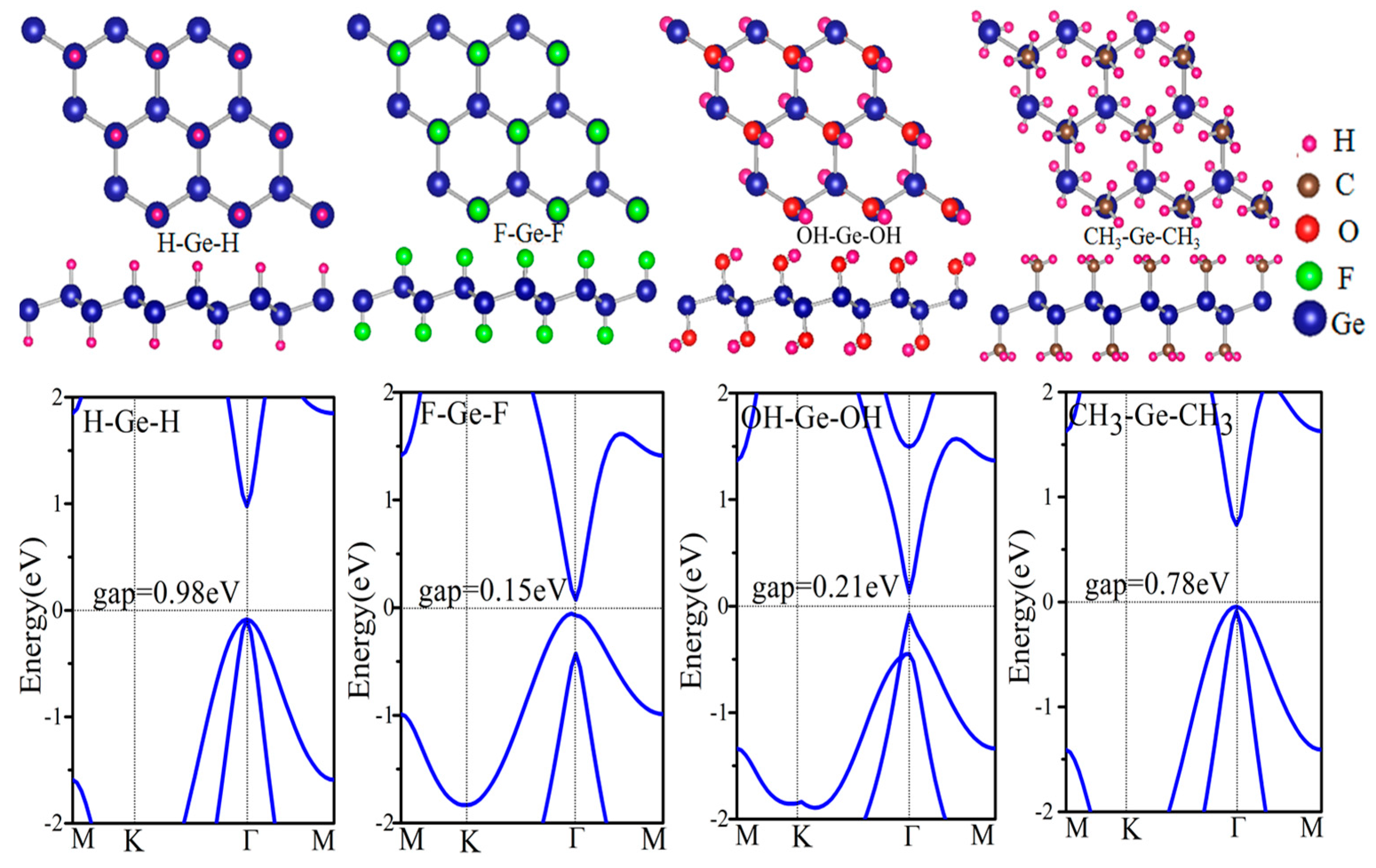
Figure 3.
The plane-integrated electron density difference, Δ(Z), for the H–Ge–H (a) and the H–Ge–H/F–Ge–F (b). Here, for panel (a), Δ𝜌(Z) = 𝜌total − 𝜌germanene − 𝜌H, in which 𝜌total, 𝜌germanene, 𝜌H are the charge densities of H–Ge–H, germanene, and H; while for panel (b), Δ𝜌(z) = 𝜌total − 𝜌H–Ge–H − 𝜌F–Ge–F where 𝜌total, 𝜌H–Ge–H, 𝜌F–Ge–F are charge densities of H–Ge–H/F–Ge–F, H–Ge–H and F–Ge–F, respectively.
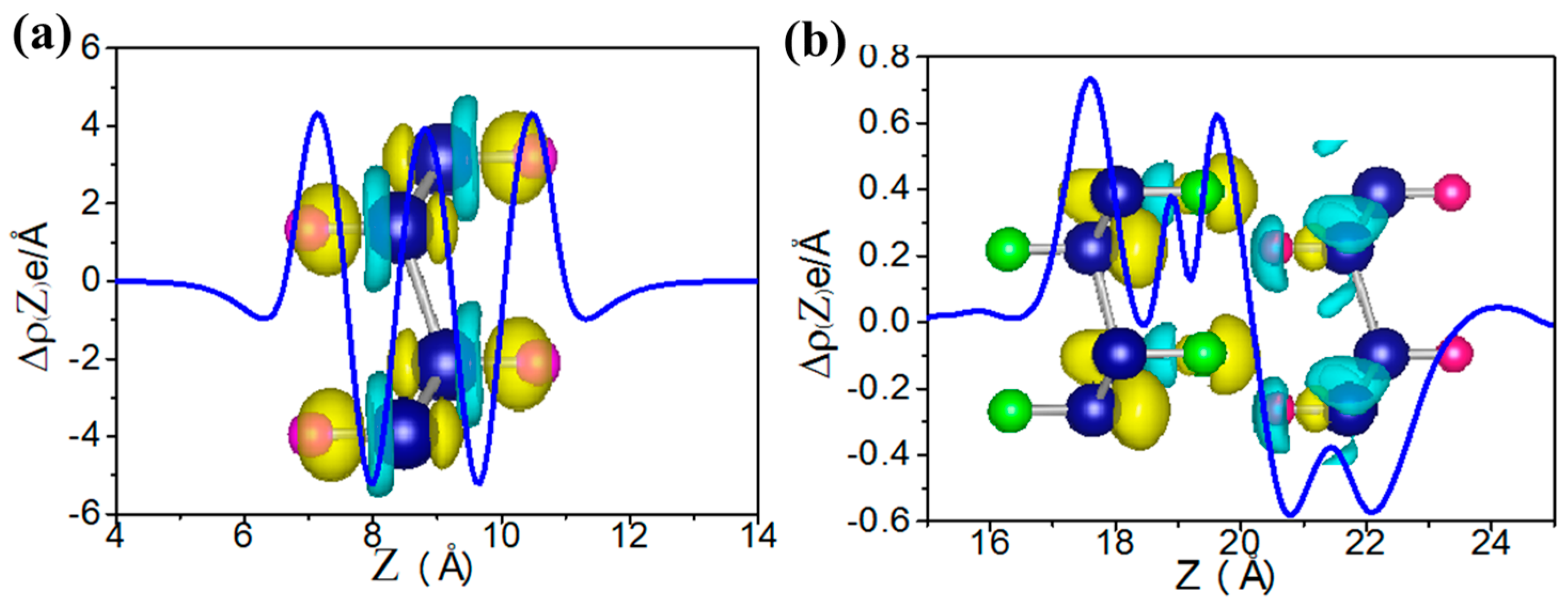
Figure 4.
The calculated band gap at Γ point (EΓ) and the global band gap (Eg) of (a) GeH; (b) GeF; (c) GeOH and (d) GeCH3 with SOC as a function of external strains. Notably, the insets in panel show the trend of band gaps of TI phase as a function of external strain.
Figure 4.
The calculated band gap at Γ point (EΓ) and the global band gap (Eg) of (a) GeH; (b) GeF; (c) GeOH and (d) GeCH3 with SOC as a function of external strains. Notably, the insets in panel show the trend of band gaps of TI phase as a function of external strain.
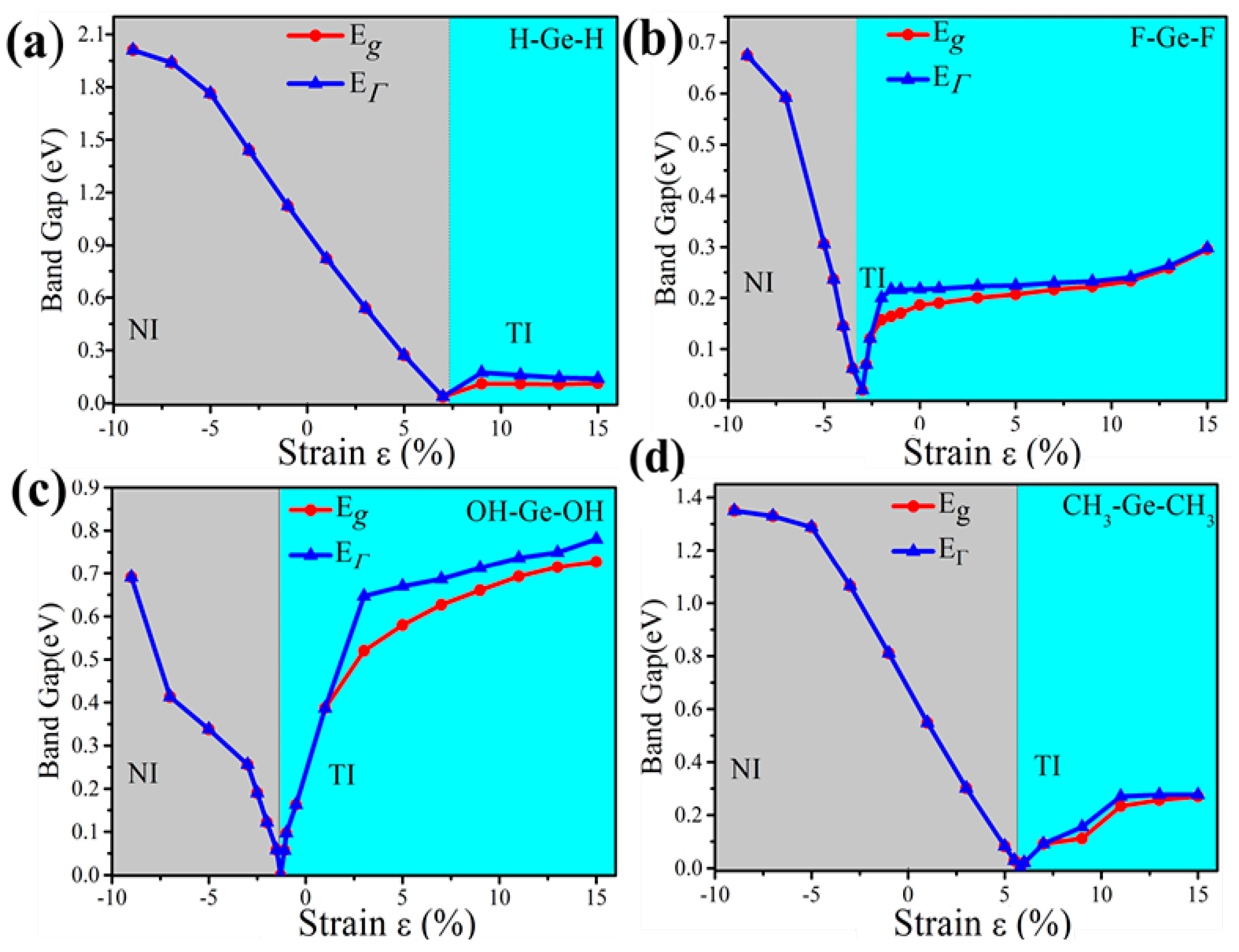
Figure 5.
Electronic band structures of GeH under the strain of 0% (a); 8% (b); and 9% (c). Panel (d) plots the evolution of the energy level of states A and B under external strain.
Figure 5.
Electronic band structures of GeH under the strain of 0% (a); 8% (b); and 9% (c). Panel (d) plots the evolution of the energy level of states A and B under external strain.
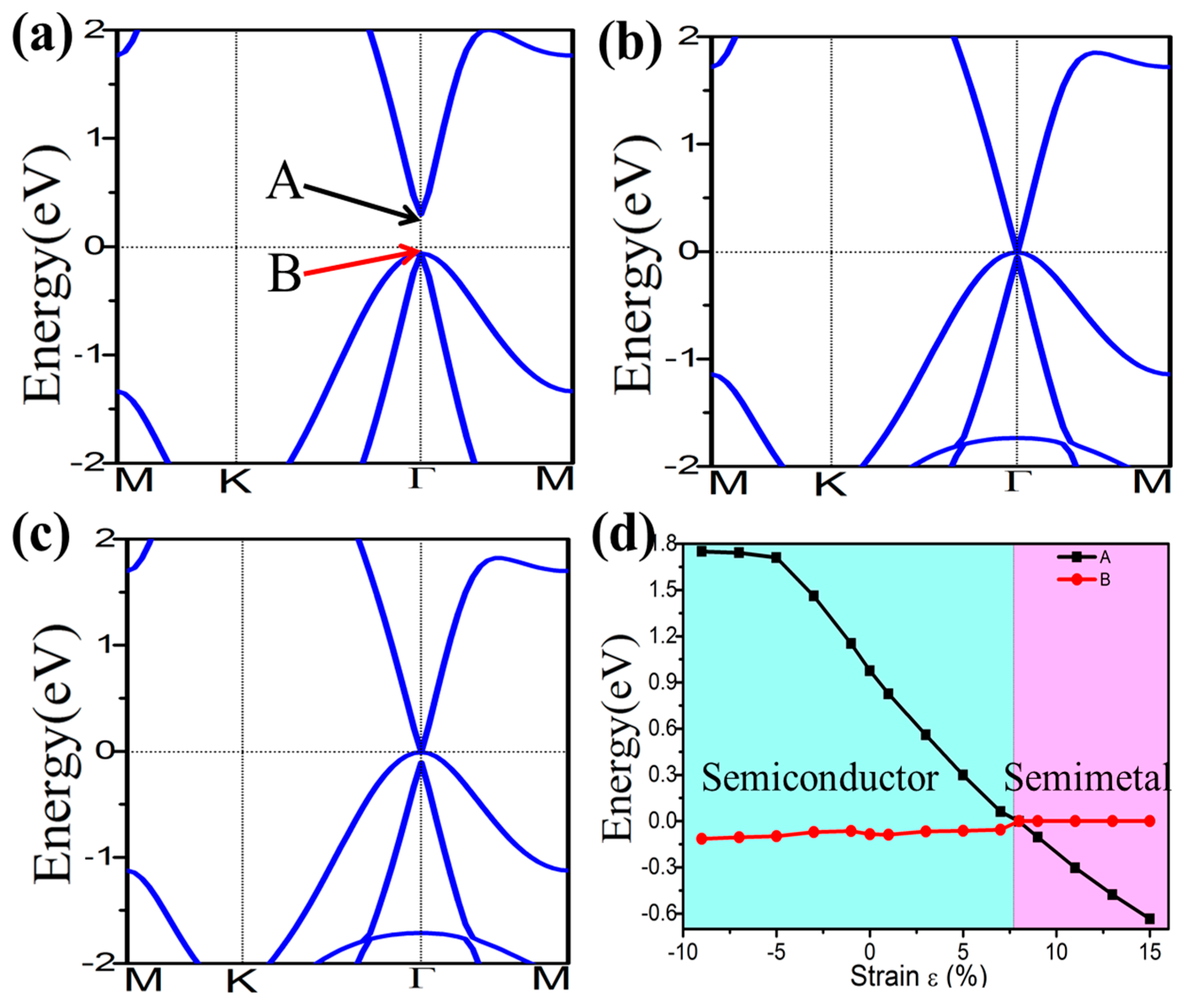
Figure 6.
Band structures for GeH without and with spin-orbit coupling SOC (a,b), and both strain of ε = 9% and SOC (c). The red and blue dots present the weights of the Ge-s and Ge-px,y orbitals, respectively. (d) Parities of occupied degenerate eigenstates at the time reversal invariant momenta (TRIM) points for GeH. Positive and negative signs denote even and odd parities, respectively.
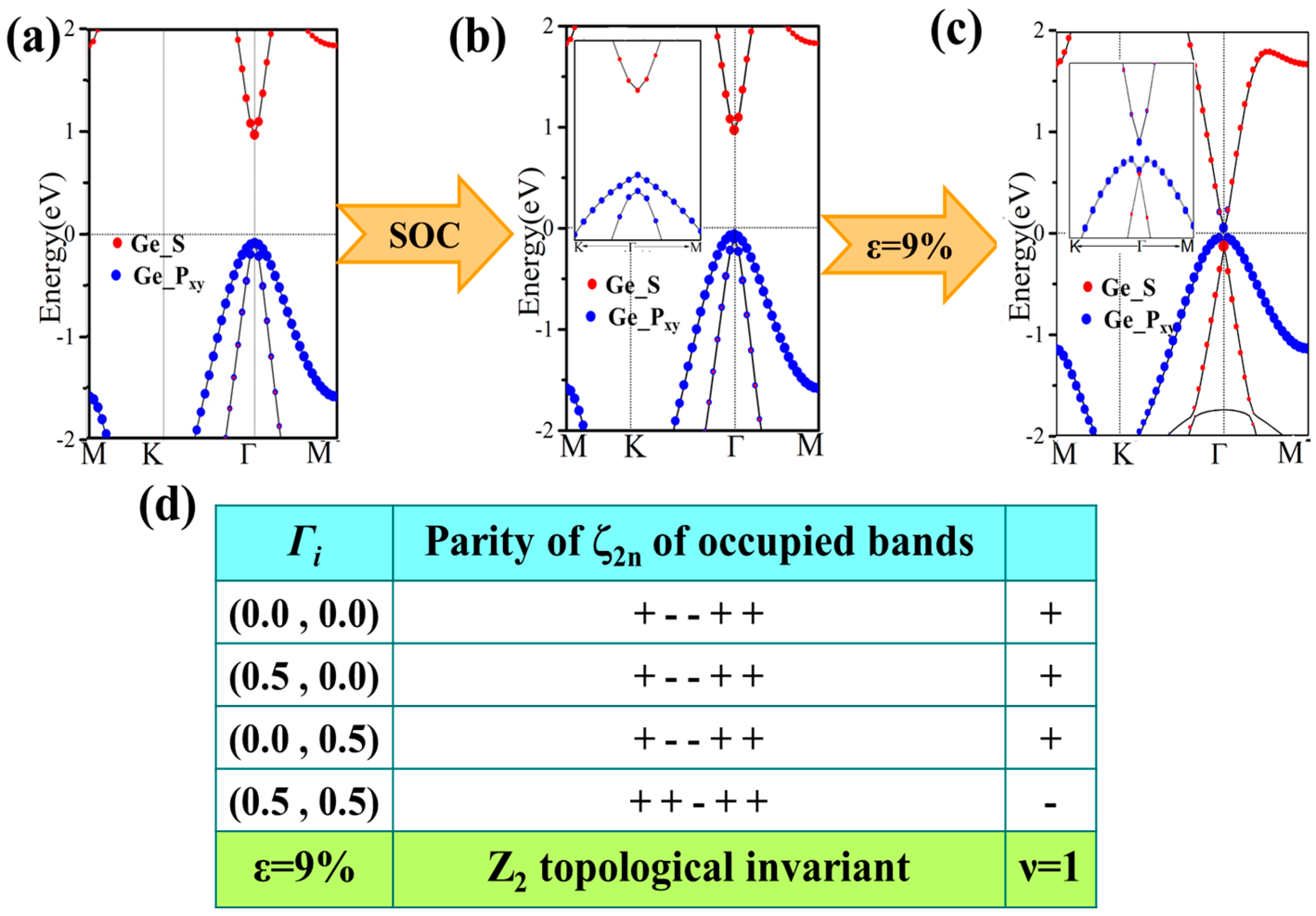
Figure 7.
(a,b) The calculated Dirac edge states, and edge spin polarization, respectively.
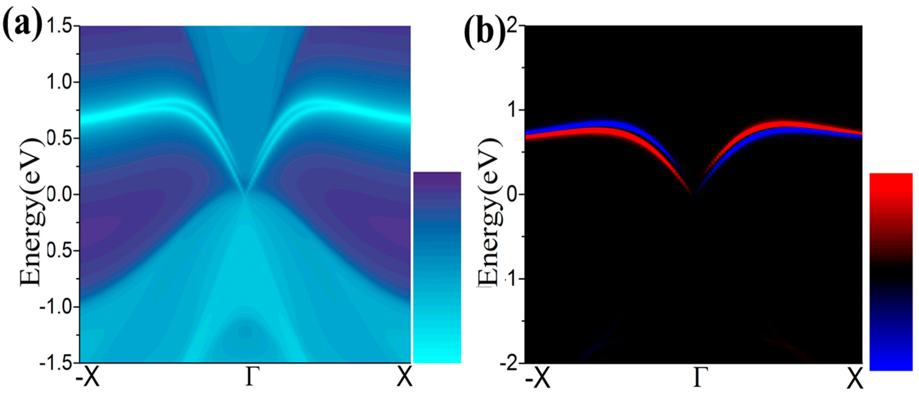
Figure 8.
The evolution of atomic s and pxy orbitals of GeH at Γ point described as crystal field splitting and SOC switched on sequence with ε = 0% and ε = 9%. The horizontal dashed lines indicate the Fermi energy.
Figure 8.
The evolution of atomic s and pxy orbitals of GeH at Γ point described as crystal field splitting and SOC switched on sequence with ε = 0% and ε = 9%. The horizontal dashed lines indicate the Fermi energy.

Figure 9.
Relaxed geometry structures of H–Ge–H/H–Ge–H, H–Ge–H/CH3–Ge–H and H–Ge–H/F–Ge–F and the corresponding energy spectra (a–c). The black line is the energy dispersion of the bilayer. The red (blue) dots represent the spectra of the isolated up (below) layer. In panel (a) red dots coincide with the blue dots.

Table 1.
Structural parameters (Å), formation energies Ef (eV per unit cell) and band gaps (eV) determined for germanene functionalized with several radicals.
Table 1.
Structural parameters (Å), formation energies Ef (eV per unit cell) and band gaps (eV) determined for germanene functionalized with several radicals.
| a (Å) | b (Å) | Ge–X/Ge–X’ (Å) | Ge–Ge (Å) | Ef (eV) | Gap (eV) | |
|---|---|---|---|---|---|---|
| Ge | 4.06 | 4.06 | \ | 2.44 | \ | 0 |
| GeH | 4.09 | 4.09 | 1.56 | 2.46 | −2.61 | 0.98 |
| GeCH3 | 4.12 | 4.12 | 2.01 | 2.50 | −4.96 | 0.78 |
| GeOH | 4.23 | 4.23 | 1.85 | 2.49 | −3.16 | 0.21 |
| GeF | 4.34 | 4.34 | 1.79 | 2.56 | −4.25 | 0.15 |
| H–Ge–CH3 | 4.10 | 4.10 | 2.01/1.56 | 2.49 | −3.82 | 0.86 |
| H–Ge–OH | 4.12 | 4.12 | 1.84/1.57 | 2.47 | −2.92 | 0.50 |
| H–Ge–F | 4.16 | 4.16 | 1.78/1.57 | 2.45 | −3.93 | 0.49 |
| CH3–Ge–OH | 4.13 | 4.15 | 2.02/1.84 | 2.51 | −4.06 | 0.44 |
| CH3–Ge–F | 4.18 | 4.18 | 2.02/1.79 | 2.51 | −4.60 | 0.41 |
| OH–Ge–F | 4.33 | 4.32 | 1.85/1.79 | 2.51 | −3.68 | 0.41 |
Table 2.
Structural parameters (Å), interlayer interaction energies (eV/Ge atom) and band gaps (eV) determined for bilayer germanene functionalized with several radicals, at full coverage.
Table 2.
Structural parameters (Å), interlayer interaction energies (eV/Ge atom) and band gaps (eV) determined for bilayer germanene functionalized with several radicals, at full coverage.
| Layer1/Layer2 | a (Å) | b (Å) | Interlayer Interaction (eV) | Gap (eV) |
|---|---|---|---|---|
| H–Ge–H/H–Ge–H | 4.09 | 4.09 | 0.013 | 0.96 |
| H–Ge–CH3/CH3–Ge–H | 4.10 | 4.10 | 0.030 | 0.86 |
| CH3–Ge–CH3/CH3–Ge–CH3 | 4.12 | 4.12 | 0.011 | 0.77 |
| H–Ge–F/F–Ge–H | 4.17 | 4.17 | 0.044 | 0.45 |
| H–Ge–HO/OH–Ge–H | 4.15 | 4.15 | 0.109 | 0.32 |
| H–Ge–H/OH–Ge–H | 4.11 | 4.11 | 0.002 | 0.48 |
| H–Ge–H/CH3-Ge-H | 4.09 | 4.10 | 0.013 | 0.18 |
| H–Ge–HO/F–Ge–H | 4.18 | 4.0 | 0.042 | 0.15 |
| H–Ge–H/F–Ge–H | 4.13 | 4.15 | 0.023 | metal |
| H–Ge–H/F–Ge–F | 4.20 | 4.17 | 0.034 | metal |
| H–Ge–F/CH3–Ge–H | 4.15 | 4.17 | 0.066 | metal |
| H–Ge–HO/CH3–Ge–H | 4.11 | 4.12 | 0.021 | metal |
| HO–Ge–H/F–Ge–H | 4.17 | 4.17 | 0.052 | metal |
© 2018 by the authors. Licensee MDPI, Basel, Switzerland. This article is an open access article distributed under the terms and conditions of the Creative Commons Attribution (CC BY) license (http://creativecommons.org/licenses/by/4.0/).
Share and Cite
MDPI and ACS Style
Ren, C.-C.; Zhang, S.-F.; Ji, W.-X.; Zhang, C.-W.; Li, P.; Wang, P.-J. Tunable Electronic and Topological Properties of Germanene by Functional Group Modification. Nanomaterials 2018, 8, 145. https://doi.org/10.3390/nano8030145
AMA Style
Ren C-C, Zhang S-F, Ji W-X, Zhang C-W, Li P, Wang P-J. Tunable Electronic and Topological Properties of Germanene by Functional Group Modification. Nanomaterials. 2018; 8(3):145. https://doi.org/10.3390/nano8030145
Chicago/Turabian StyleRen, Ceng-Ceng, Shu-Feng Zhang, Wei-Xiao Ji, Chang-Wen Zhang, Ping Li, and Pei-Ji Wang. 2018. "Tunable Electronic and Topological Properties of Germanene by Functional Group Modification" Nanomaterials 8, no. 3: 145. https://doi.org/10.3390/nano8030145
Note that from the first issue of 2016, this journal uses article numbers instead of page numbers. See further details here.