Nanostructure Formation on Diamond-Like Carbon Films Induced with Few-Cycle Laser Pulses at Low Fluence from a Ti:Sapphire Laser Oscillator


Abstract
:1. Introduction
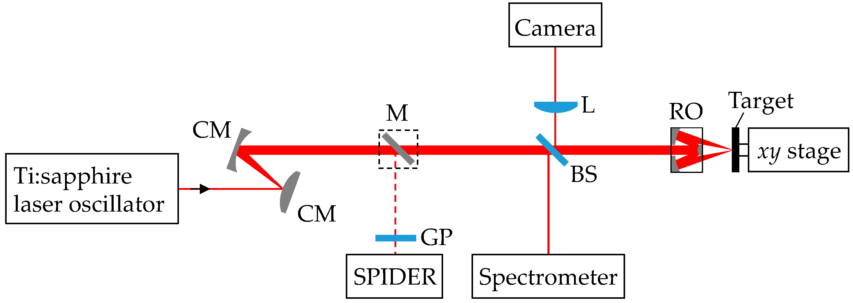
2. Experimental
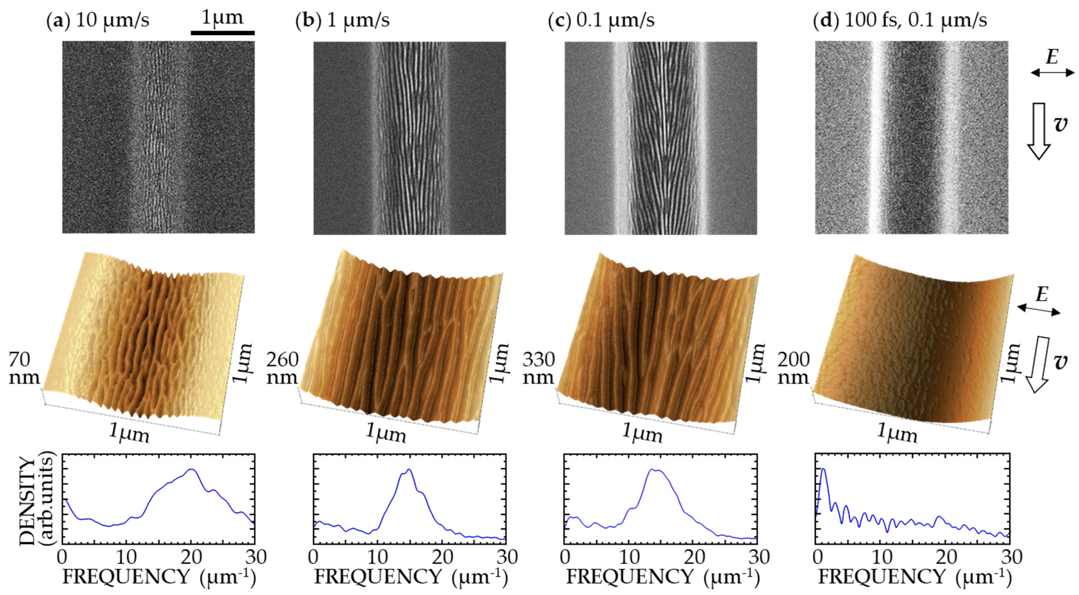
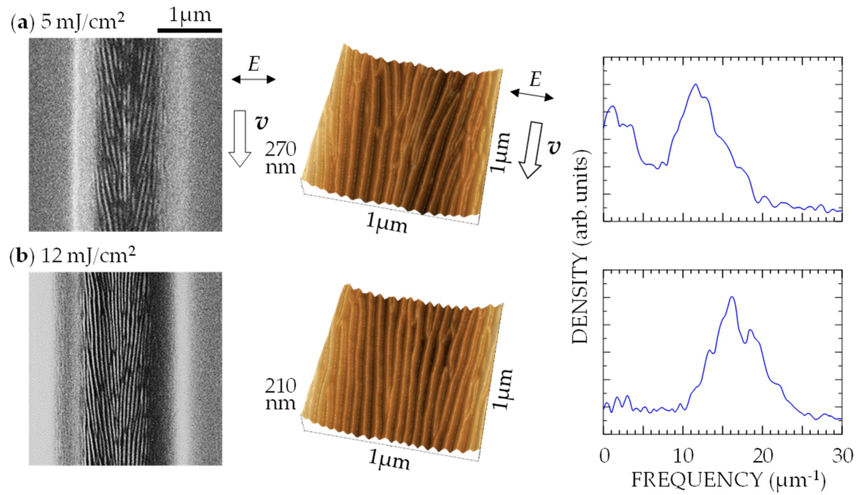
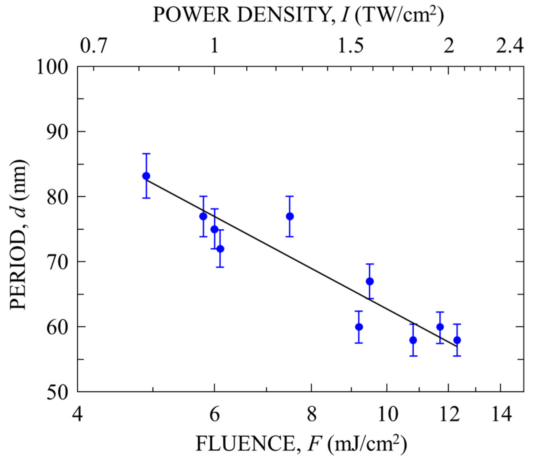
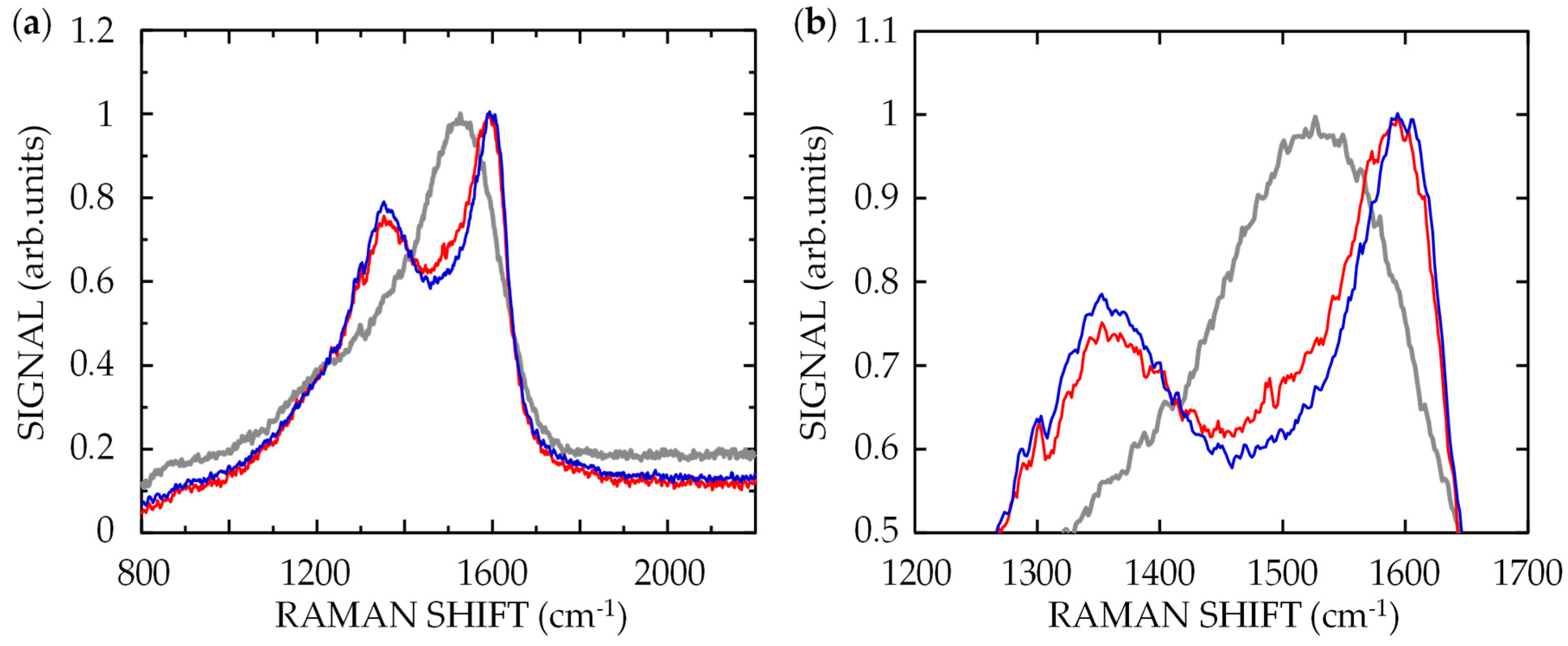
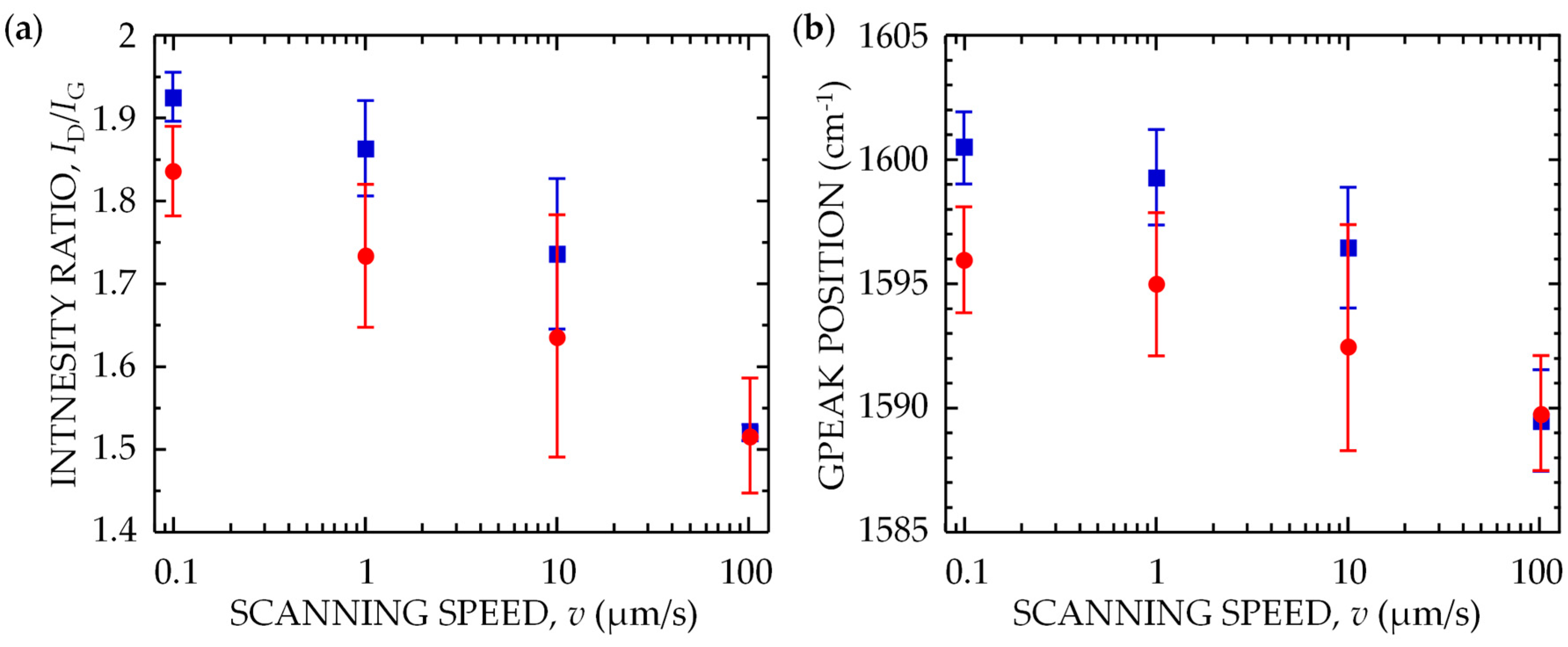
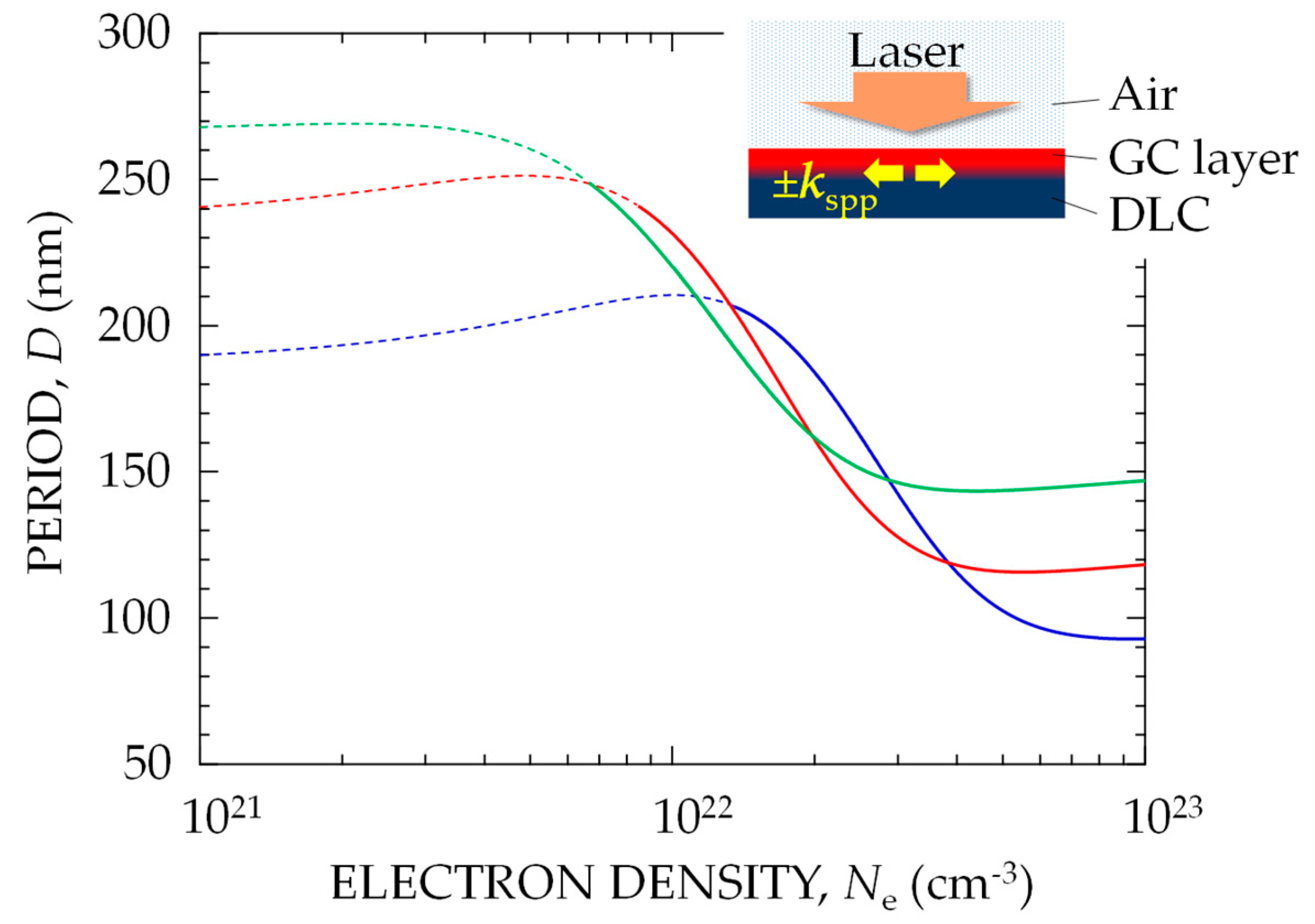
3. Results and Discussion
4. Conclusions
Author Contributions
Funding
Acknowledgments
Conflicts of Interest
References and Note
- Bonse, J.; Sturm, H.; Schmidt, D.; Kautek, W. Chemical, morphological and accumulation phenomena in ultrashort-pulse laser ablation of TiN in air. Appl. Phys. A Mater. Sci. Process. 2000, 71, 657–665. [Google Scholar] [CrossRef]
- Reif, J.; Costache, F.; Henyk, M.; Pandelov, S.V. Ripples revisited: Non-classical morphology at the bottom of femtosecond laser ablation craters in transparent dielectrics. Appl. Surf. Sci. 2002, 197–198, 891–895. [Google Scholar] [CrossRef]
- Yasumaru, N.; Miyazaki, K.; Kiuchi, J. Femtosecond-laser-induced nanostructure formed on hard thin films of TiN and DLC. Appl. Phys. A Mater. Sci. Process. 2003, 76, 983–985. [Google Scholar] [CrossRef]
- Wu, Q.; Ma, Y.; Fang, R.; Liao, Y.; Yu, Q. Femtosecond laser-induced periodic surface structure on diamond film. Appl. Phys. Lett. 2003, 82, 1703–1705. [Google Scholar] [CrossRef]
- Borowiec, A.; Haugen, H.K. Subwavelength ripple formation on the surfaces of compound semiconductors irradiated with femtosecond laser pulses. Appl. Phys. Lett. 2003, 82, 4462–4464. [Google Scholar] [CrossRef]
- Daminelli, G.; Krüger, J.; Kautek, W. Femtosecond laser interaction with silicon under water confinement. Thin Solid Films 2004, 467, 334–341. [Google Scholar] [CrossRef]
- Bonse, J.; Krüger, J. Femtosecond laser-induced periodic surface structures. J. Appl. Phys. 2012, 24, 042006-1–042006-7. [Google Scholar] [CrossRef]
- Miyazaki, K.; Miyaji, G. Mechanism and control of periodic surface nanostructure formation with femtosecond laser pulses. Appl. Phys. A Mater. Sci. Process. 2014, 114, 177–185. [Google Scholar] [CrossRef] [Green Version]
- Miyazaki, K.; Miyaji, G.; Inoue, T. Nanograting formation on metals in air with interfering femtosecond laser pulses. Appl. Phys. Lett. 2015, 107, 071103. [Google Scholar] [CrossRef] [Green Version]
- Miyaji, G.; Miyazaki, K. Fabrication of 50-nm period gratings on GaN in air through plasmonic near-field ablation induced by ultraviolet femtosecond laser pulses. Opt. Express 2016, 24, 4648–4653. [Google Scholar] [CrossRef] [PubMed]
- Yasumaru, N.; Miyazaki, K.; Kiuchi, J. Glassy carbon layer formed in diamond-like carbon films with femtosecond laser pulses. Appl. Phys. A Mater. Sci. Process. 2004, 79, 425–427. [Google Scholar] [CrossRef]
- Miyazaki, K.; Maekawa, N.; Kobayashi, W.; Kaku, M.; Yasumaru, N.; Kiuchi, J. Reflectivity in femtosecond-laser-induced structural changes of diamond-like carbon film. Appl. Phys. A Mater. Sci. Process. 2005, 80, 17–21. [Google Scholar] [CrossRef]
- Miyaji, G.; Miyazaki, K. Ultrafast dynamics of periodic nanostructure formation on diamond-like carbon films irradiated with femtosecond laser pulses. Appl. Phys. Lett. 2006, 89, 191902. [Google Scholar] [CrossRef] [Green Version]
- Miyaji, G.; Miyazaki, K. Nanoscale ablation on patterned diamond-like carbon film with femtosecond laser pulses. Appl. Phys. Lett. 2007, 91, 123102. [Google Scholar] [CrossRef] [Green Version]
- Miyaji, G.; Miyazaki, K. Origin of periodicity in nanostructuring on thin film surfaces ablated with femtosecond laser pulses. Opt. Express 2008, 16, 16265–16271. [Google Scholar] [CrossRef] [PubMed]
- Miyaji, G.; Miyazaki, K.; Zhang, K.; Yoshifuji, T.; Fujita, J. Mechanism of femtosecond-laser-induced periodic nanostructure formation on crystalline silicon surface immersed in water. Opt. Express 2012, 20, 14848–14856. [Google Scholar] [CrossRef] [PubMed]
- Miyazaki, K.; Miyaji, G. Nanograting formation through surface plasmon fields induced by femtosecond laser pulses. J. Appl. Phys. 2013, 114, 153108. [Google Scholar] [CrossRef] [Green Version]
- Miyaji, G.; Miyazaki, K. Shaping of nanostructured surface in femtosecond laser ablation of thin films. Appl. Phys. A Mater. Sci. Process. 2010, 98, 927–930. [Google Scholar] [CrossRef]
- Kärtner, F.X.; Morgner, U.; Schibli, T.; Ell, R.; Haus, H.A.; Fujimoto, J.G.; Ippen, E.P. Few-Cycle Pulses Directly from a Laser. In Few-Cycle Laser Pulse Generation and Its Applications, 1st ed.; Kärtner, F.X., Ed.; Springer: Berlin/Heidelberg, Germany, 2004; pp. 73–136. ISBN 978-3-540-20115-1. [Google Scholar]
- Raether, H. Surface Plasmons on Smooth and Rough Surfaces and on Gratings; Springer-Verlag: Heidelberg, Germany, 1988; ISBN 978-3-540-47441-8. [Google Scholar]
- Yoshikawa, M.; Katagiri, G.; Ishida, H.; Ishitani, A. Raman spectra of diamondlike amorphous carbon films. J. Appl. Phys. 1988, 64, 6464–6468. [Google Scholar] [CrossRef]
- Zhang, S.; Zeng, X.T.; Xie, H.; Hing, P. A phenomenological approach for the Id/Ig ratio and sp3 fraction of magnetron sputtered a-C films. Surf. Coat. Technol. 2000, 123, 256–260. [Google Scholar] [CrossRef]
- Robertson, J. Diamond-like amorphous carbon. Mater. Sci. Eng. 2002, R37, 129–281. [Google Scholar] [CrossRef]
- Tai, F.C.; Lee, S.C.; Wei, C.H.; Tyan, S.L. Correlation between ID/IG Ratio from Visible Raman Spectra and sp2/sp3 Ratio from XPS Spectra of Annealed Hydrogenated DLC Film. Mater. Trans. 2006, 47, 1847–1852. [Google Scholar] [CrossRef]
- Tuinstra, F.; Koenig, J.L. Raman Spectrum of Graphite. J. Chem. Phys. 1970, 53, 1126–1130. [Google Scholar] [CrossRef]
- Nemanich, R.J.; Solin, S.A. First- and second-order Raman scattering from finite-size crystals of graphite. Phys. Rev. B 1979, 20, 392–400. [Google Scholar] [CrossRef]
- Yoshikawa, M.; Nagai, N.; Matsuki, M.; Fukuda, H.; Katagiri, G.; Ishida, H.; Ishitani, A.; Nagai, I. Raman scattering from sp2 carbon clusters. Phys. Rev. B 1992, 46, 7169–7174. [Google Scholar] [CrossRef]
- Ferrari, A.C.; Robertson, J. Interpretation of Raman spectra of disordered and amorphous carbon. Phys. Rev. B 2000, 61, 14095–14107. [Google Scholar] [CrossRef]
- Wojdyr, M. Fityk: A general-purpose peak fitting program. J. Appl. Crystal. 2010, 43, 1126–1128. [Google Scholar] [CrossRef]
- Miyaji, G.; Miyazaki, K. Role of multiple shots of femtosecond laser pulses in periodic surface nanoablation. Appl. Phys. Lett. 2013, 103, 071910. [Google Scholar] [CrossRef]
- Sokolowski-Tinten, K.; Linde, D. Generation of dense electron-hole plasmas in silicon. Phys. Rev. B 2000, 61, 2643–2650. [Google Scholar] [CrossRef]
- Because the Drude damping time of the DLC films or GC was never measured, we used the value of Si reported in Ref. 31. Using the time in a range of 1–10 fs, we confirmed that the calculation results were almost the same as that with the time of 1 fs.
- Alterovitz, S.A.; Savvides, N.; Smith, F.W.; Woollam, J.A. Amorphous Hydrogenated “Diamondlike” Carbon Films and Arc-Evaporated Carbon Films. In Handbook of Optical Constants of Solids; Palik, E.D., Ed.; Academic Press: San Diego, CA, USA, 1985; pp. 838–852. ISBN 978-0-125-44423-1. [Google Scholar]
- Rebollar, E.; Pérez, S.; Hernández, J.J.; Martín-Fabiani, I.; Rueda, D.R.; Ezquerra, T.A.; Castillejo, M. Assessment and Formation Mechanism of Laser-Induced Periodic Surface Structures on Polymer Spin-Coated Films in Real and Reciprocal Space. Langmuir 2011, 27, 5596–5606. [Google Scholar] [CrossRef] [PubMed] [Green Version]
- Rebollar, E.; Rueda, D.R.; Martín-Fabiani, I.; Rodríguez-Rodríguez, Á.; García-Gutiérrez, M.-C.; Portale, G.; Castillejo, M.; Ezquerra, T.A. In Situ Monitoring of Laser-Induced Periodic Surface Structures Formation on Polymer Films by Grazing Incidence Small-Angle X-ray Scattering. Langmuir 2015, 31, 3973–3981. [Google Scholar] [CrossRef] [PubMed] [Green Version]
- Roth, S.V.; Döhrmann, R.; Gehrke, R.; Röhlsberger, R.; Schlage, K.; Metwalli, E.; Körstgens, V.; Burghammer, M.; Riekel, C.; David, C.; et al. Mapping the morphological changes of deposited gold nanoparticles across an imprinted groove. J. Appl. Crystallogr. 2015, 48, 1827–1833. [Google Scholar] [CrossRef]


© 2018 by the authors. Licensee MDPI, Basel, Switzerland. This article is an open access article distributed under the terms and conditions of the Creative Commons Attribution (CC BY) license (http://creativecommons.org/licenses/by/4.0/).
Share and Cite
Nikaido, S.; Natori, T.; Saito, R.; Miyaji, G. Nanostructure Formation on Diamond-Like Carbon Films Induced with Few-Cycle Laser Pulses at Low Fluence from a Ti:Sapphire Laser Oscillator. Nanomaterials 2018, 8, 535. https://doi.org/10.3390/nano8070535
Nikaido S, Natori T, Saito R, Miyaji G. Nanostructure Formation on Diamond-Like Carbon Films Induced with Few-Cycle Laser Pulses at Low Fluence from a Ti:Sapphire Laser Oscillator. Nanomaterials. 2018; 8(7):535. https://doi.org/10.3390/nano8070535
Chicago/Turabian StyleNikaido, Seiya, Takumi Natori, Ryo Saito, and Godai Miyaji. 2018. "Nanostructure Formation on Diamond-Like Carbon Films Induced with Few-Cycle Laser Pulses at Low Fluence from a Ti:Sapphire Laser Oscillator" Nanomaterials 8, no. 7: 535. https://doi.org/10.3390/nano8070535