Structure–Function Correlations in Sputter Deposited Gold/Fluorocarbon Multilayers for Tuning Optical Response

 , and
, and
Abstract
:
1. Introduction
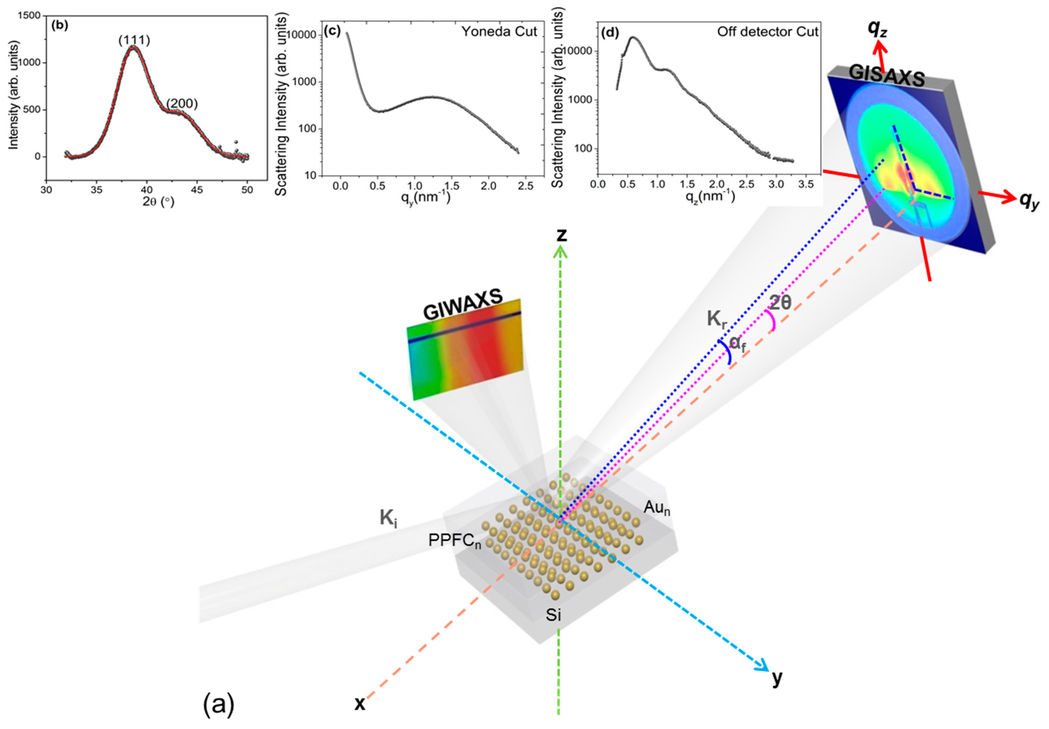
2. Experimental Details
2.1. Sample Preparation
2.2. Characterization
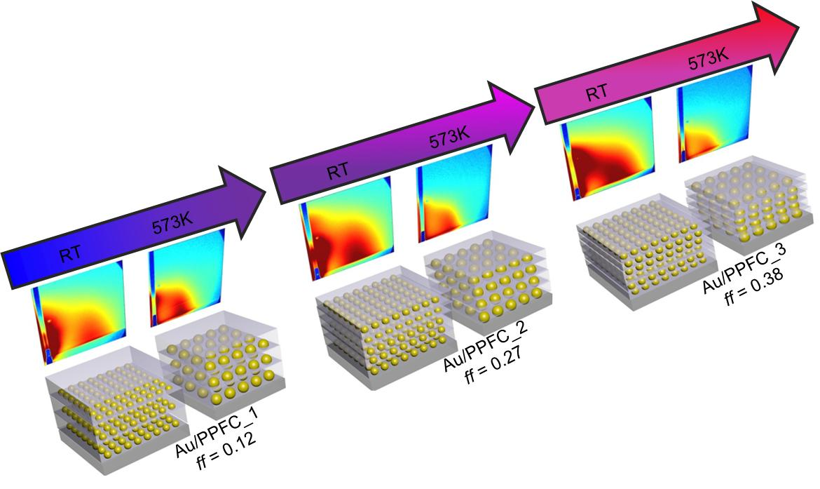
3. Results and Discussion
3.1. Structural Properties at Room Temperature
3.2. GIWAXS
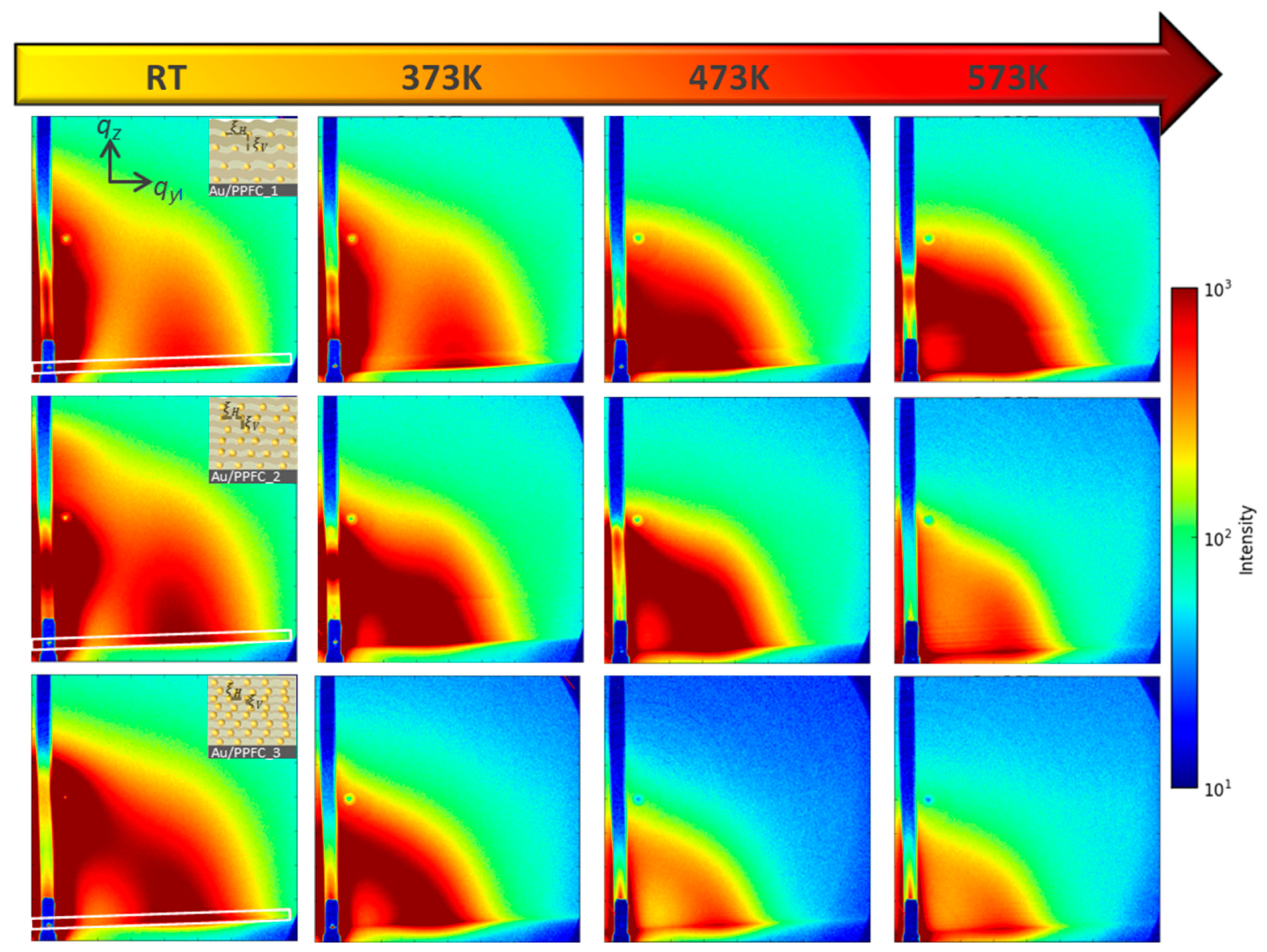
3.3. GISAXS
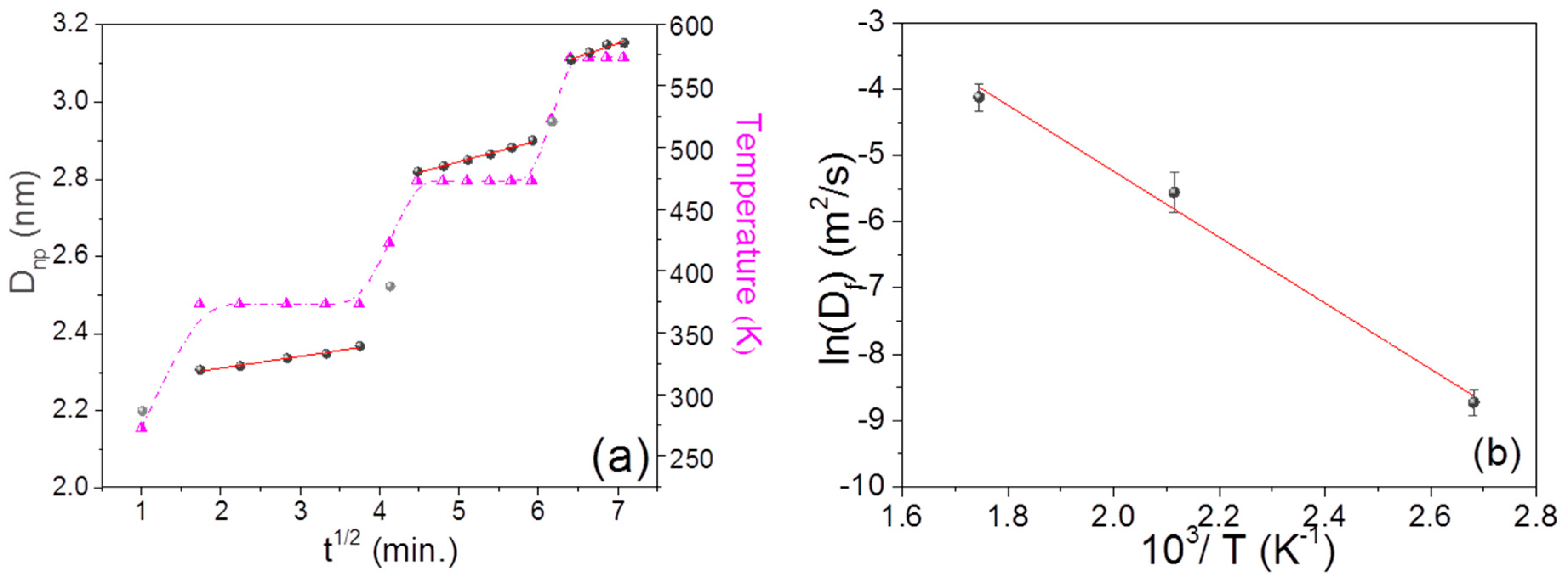
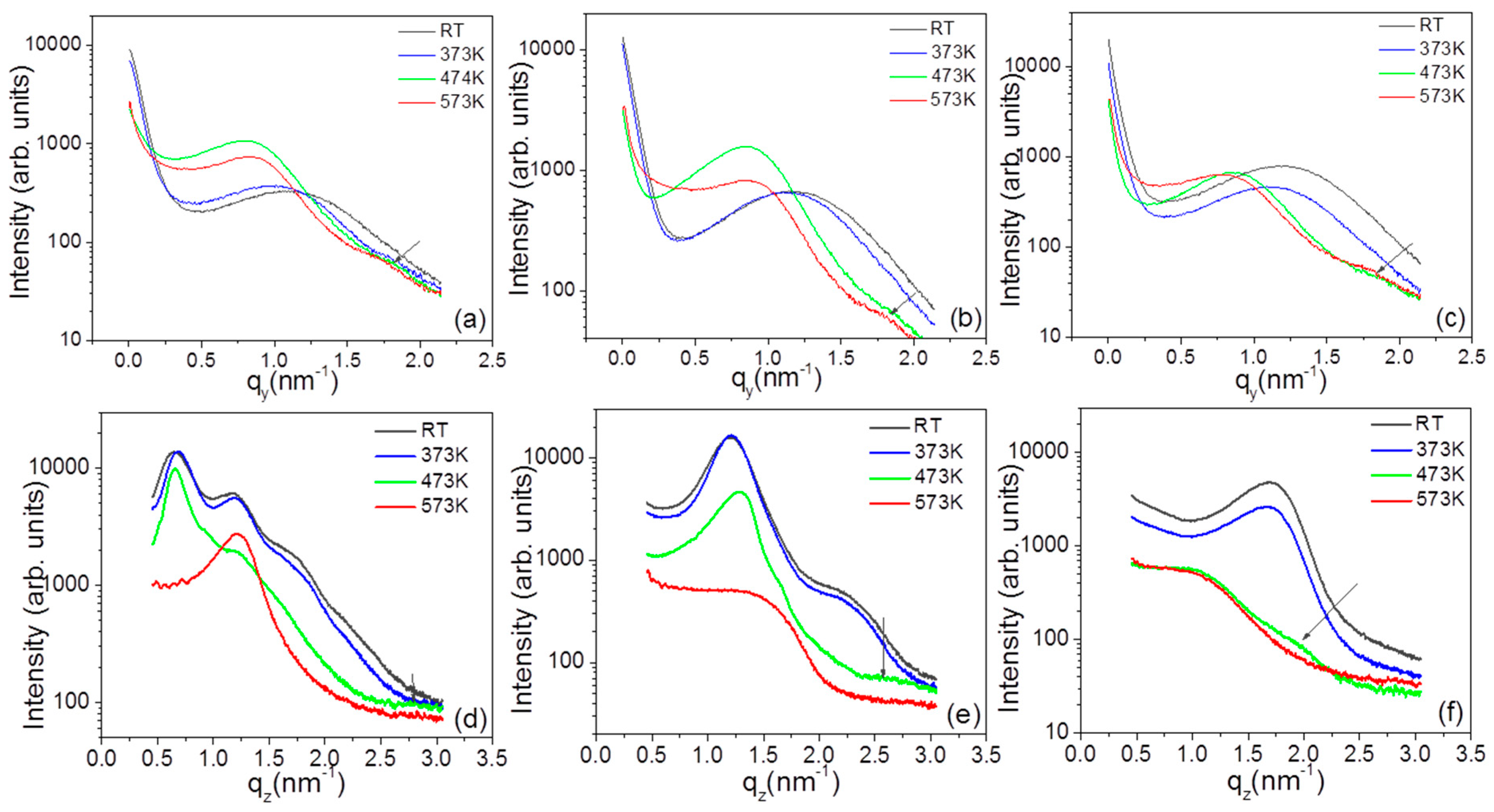
3.4. Structural Changes during and after Annealing
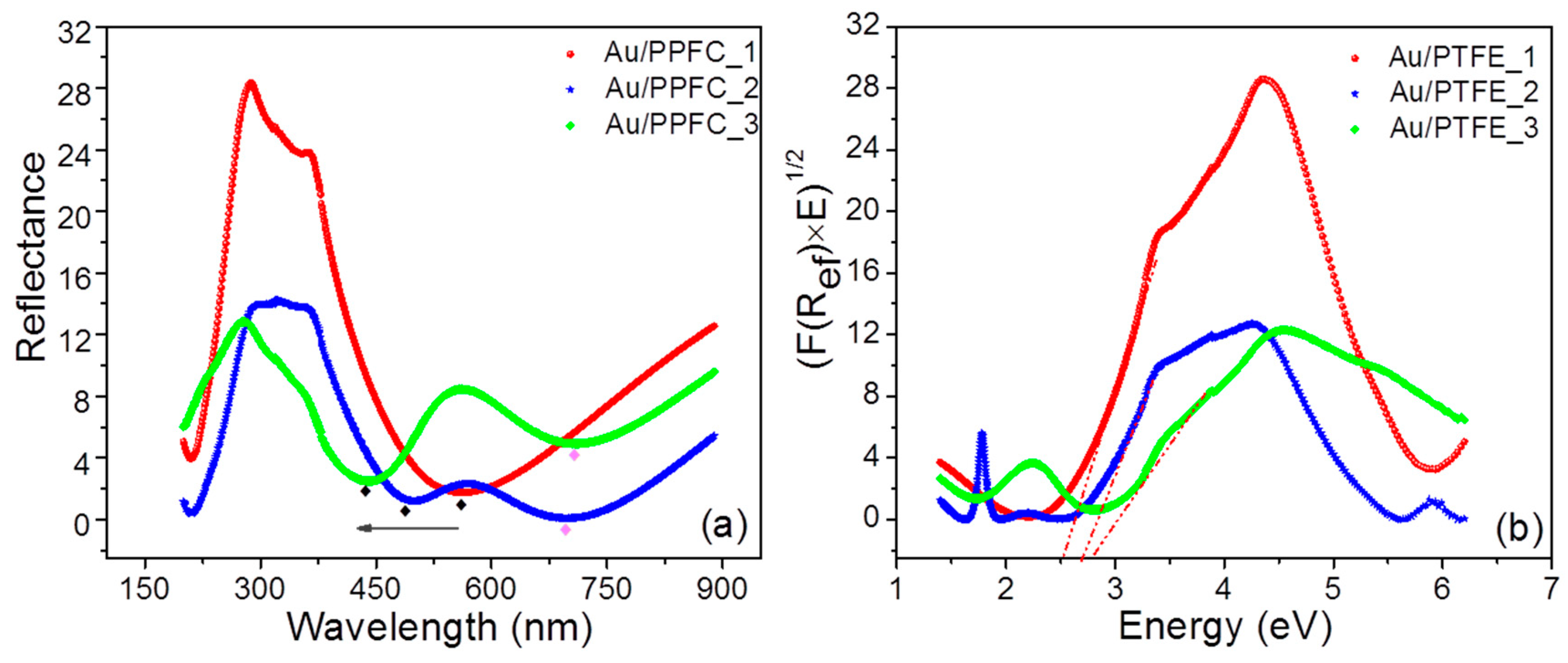
3.5. Optical Properties at Room Temperature
3.6. Temperature-Dependent Optical Response
4. Conclusions
Supplementary Materials
Author Contributions
Funding
Conflicts of Interest
References
- Faupel, F.; Zaporojtchenko, V.; Strunskus, T.; Elbahri, M. Faupel.pdf. Adv. Eng. Mater. 2010, 12, 1177–1190. [Google Scholar] [CrossRef]
- Sanchez, C.; Belleville, P.; Popall, M.; Nicole, L. Applications of advanced hybrid organic–inorganic nanomaterials: From laboratory to market. Chem. Soc. Rev. 2011, 40, 696–753. [Google Scholar] [CrossRef] [PubMed]
- Srivastava, S.; Haridas, M.; Basu, J.K. Optical properties of polymer nanocomposites. Bull. Mater. Sci. 2008, 31, 213–217. [Google Scholar] [CrossRef]
- Lopes, W.A.; Jaeger, H.M. Hierarchical self-assembly of metal nanostrucures on diblock copolymer scaffolds. Nature 2001, 414, 735–738. [Google Scholar] [CrossRef] [PubMed]
- Turković, A.; Dubček, P.; Juraić, K.; Drašner, A.; Bernstorff, S. SAXS Studies of Tio2 nanoparticles in polymer electrolytes and in nanostructured films. Materials 2010, 3, 4979–4993. [Google Scholar] [CrossRef] [PubMed]
- Schwartzkopf, M.; Santoro, G.; Brett, C.J.; Rothkirch, A.; Polonskyi, O.; Hinz, A.; Metwalli, E.; Yao, Y.; Strunskus, T.; Faupel, F.; et al. Real-time monitoring of morphology and optical properties during sputter deposition for tailoring metal–polymer interfaces. ACS Appl. Mater. Interfaces 2015, 7, 13547–13556. [Google Scholar] [CrossRef] [PubMed]
- Alsawafta, M.; Badilescu, S.; Paneri, A.; Van Truong, V.; Packirisamy, M. Gold-poly(methyl methacrylate) nanocomposite films for plasmonic biosensing applications. Polymers 2011, 3, 1833–1848. [Google Scholar] [CrossRef]
- Roth, S.V.; Santoro, G.; Risch, J.F.H.; Yu, S.; Schwartzkopf, M.; Boese, T.; Döhrmann, R.; Zhang, P.; Besner, B.; Bremer, P.; et al. Patterned diblock co-polymer thin films as templates for advanced anisotropic metal nanostructures. ACS Appl. Mater. Interfaces 2015, 7, 12470–12477. [Google Scholar] [CrossRef]
- Hua, Y.; Chandra, K.; Dam, D.H.M.; Wiederrecht, G.P.; Odom, T.W. Shape-dependent nonlinear optical properties of anisotropic gold nanoparticles. J. Phys. Chem. Lett. 2015, 6, 4904–4908. [Google Scholar] [CrossRef]
- Torrisi, V.; Ruffino, F. Metal–polymer nanocomposites: (Co-)evaporation/(Co)sputtering approaches and electrical properties. Coatings 2015, 5, 378–424. [Google Scholar] [CrossRef]
- Ciprari, D.; Jacob, K.; Tannenbaum, R. Characterization of polymer nanocomposite interphase and its impact on mechanical properties. Macromolecules 2006, 39, 6565–6573. [Google Scholar] [CrossRef]
- Li, S.; Meng Lin, M.; Toprak, M.S.; Kim, D.K.; Muhammed, M. Nanocomposites of polymer and inorganic nanoparticles for optical and magnetic applications. Nano Rev. 2010, 1, 5214. [Google Scholar] [CrossRef] [PubMed]
- Shen, Y.; Lin, Y.; Nan, C.W. Interfacial effect on dielectric properties of polymer nanocomposites filled with core/shell-structured particles. Adv. Funct. Mater. 2007, 17, 2405–2410. [Google Scholar] [CrossRef]
- Cao, G.Z. Nanostructures Nanomaterials: Synthesis, Properties Applications, 2nd ed.; Imperial College Press: London, UK, 2004; ISBN 1-86094-4159. [Google Scholar]
- Takele, H.; Schürmann, U.; Greve, H.; Paretkar, D.; Zaporojtchenko, V.; Faupel, F. Controlled growth of Au nanoparticles in co-evaporated metal/polymer composite films and their optical and electrical properties. Eur. Phys. J. Appl. Phys. 2006, 33, 83–89. [Google Scholar] [CrossRef]
- Schwartzkopf, M.; Buffet, A.; Körstgens, V.; Metwalli, E.; Schlage, K.; Benecke, G.; Perlich, J.; Rawolle, M.; Rothkirch, A.; Heidmann, B.; et al. From atoms to layers: In situ gold cluster growth kinetics during sputter deposition. Nanoscale 2013, 5, 5053. [Google Scholar] [CrossRef] [PubMed]
- Kelly, K.L.; Coronado, E.; Zhao, L.L.; Schatz, G.C. The optical properties of metal nanoparticles: The influence of size, shape, and dielectric environment. J. Phys. Chem. B 2003, 107, 668–677. [Google Scholar] [CrossRef]
- Heilmann, A. Polymer Films with Embedded Metal Nanoparticles; Springer: Berlin, Germany, 2003; ISBN 978-3540431510. [Google Scholar]
- Zaporojtchenko, V.; Podschun, R.; Schürmann, U.; Kulkarni, A.; Faupel, F. Physico-chemical and antimicrobial properties of co-sputtered Ag-Au/PTFE nanocomposite coatings. Nanotechnology 2006, 17, 4904–4908. [Google Scholar] [CrossRef]
- Kim, S.H.; Kim, M.; Lee, J.H.; Lee, S.-J. Self-cleaning transparent heat mirror with a plasma polymer fluorocarbon thin film fabricated by a continuous roll-to-roll sputtering process. ACS Appl. Mater. Interfaces 2018, 10, 10454–10460. [Google Scholar] [CrossRef]
- Lahav, M.; Vaskevich, A.; Rubinstein, I. Biological sensing using transmission surface plasmon resonance spectroscopy. Langmuir 2004, 20, 7365–7367. [Google Scholar] [CrossRef]
- Zekonyte, J.; Zaporojtchenko, V.; Faupel, F. Investigation of the drastic change in the sputter rate of polymers at low ion fluence. Nucl. Instrum. Methods Phys. Res. B 2005, 236, 241–248. [Google Scholar] [CrossRef]
- Lei, Y.; Mehmood, F.; Lee, S.; Greeley, J.; Lee, B.; Seifert, S.; Winans, R.E.; Elam, J.W.; Meyer, R.J.; Redfern, P.C.; et al. Increased silver activity for direct. Science 2010, 328, 224–228. [Google Scholar] [CrossRef] [PubMed]
- Vegso, K.; Siffalovic, P.; Benkovicova, M.; Jergel, M.; Luby, S.; Majkova, E.; Capek, I.; Kocsis, T.; Perlich, J.; Roth, S.V. GISAXS analysis of 3D nanoparticle assemblies—effect of vertical nanoparticle ordering. Nanotechnology 2012, 23, 045704. [Google Scholar] [CrossRef] [PubMed]
- Müller-Buschbaum, P. Applications of Synchrotron light to scattering and diffraction in materials and life sciences: A basic introduction to grazing incidence small-angle X-ray scattering. Lect. Notes Phys. 2009, 776, 61–89. [Google Scholar]
- Hexemer, A.; Müller-Buschbaum, P. Advanced grazing-incidence techniques for modern soft-matter materials analysis. IUCrJ 2015, 2, 106–125. [Google Scholar] [CrossRef] [PubMed]
- Choi, J.; Choi, M.-J.; Yoo, J.-K.; Park, W.I.; Lee, J.H.; Lee, J.Y.; Jung, Y.S. Localized surface plasmon-enhanced nanosensor platform using dual-responsive polymer nanocomposites. Nanoscale 2013, 5, 7403. [Google Scholar] [CrossRef] [PubMed]
- Novotny, L.; Hecht, B. Surface plasmon. In Principles of Nano-Optics; Cambridge University Press: Cambridge, UK, 2012; pp. 407–450. ISBN 9780511813535. [Google Scholar]
- Pandit, P.; Banerjee, M.; Pandey, K.K.; Sharma, S.M.; Gupta, A. Role of substrate in melting behavior of Langmuir-Blodgett films. Colloids Surf. A Physicochem. Eng. Asp. 2015, 471, 159–163. [Google Scholar] [CrossRef]
- Amenitsch, H.; Bernstorff, S.; Kriechbaum, M.; Lombardo, D.; Mio, H.; Rappolt, M.; Laggner, P. Performance and first results of the ELETTRA high-flux beamline for small-angle X-ray scattering. J. Appl. Crystallogr. 1997, 30, 872–876. [Google Scholar] [CrossRef]
- Bushroa, A.R.; Rahbari, R.G.; Masjuki, H.H.; Muhamad, M.R. Approximation of crystallite size and microstrain via XRD line broadening analysis in TiSiN thin films. Vacuum 2012, 86, 1107–1112. [Google Scholar] [CrossRef]
- Davey, W.P. Precision measurements of the lattice constants of twelve common metals. Phys. Rev. 1925, 538, 753–761. [Google Scholar] [CrossRef]
- Benecke, G.; Wagermaier, W.; Li, C.; Schwartzkopf, M.; Flucke, G.; Hoerth, R.; Zizak, I.; Burghammer, M.; Metwalli, E.; Müller-Buschbaum, P.; et al. A customizable software for fast reduction and analysis of large X-ray scattering data sets: Applications of the new DPDAK package to small-angle X-ray scattering and grazing-incidence small-angle X-ray scattering. J. Appl. Crystallogr. 2014, 47, 1797–1803. [Google Scholar] [CrossRef]
- Levine, J.R.; Cohen, J.B.; Chung, Y.W. Thin film island growth kinetics: A grazing incidence small angle X-ray scattering study of gold on glass. Surf. Sci. 1991, 248, 215–224. [Google Scholar] [CrossRef]
- Babonneau, D.; Petroff, F.; Maurice, J.L.; Fettar, F.; Vaurès, A.; Naudon, A. Evidence for a self-organized growth in granular Co/Al2O3 multilayers. Appl. Phys. Lett. 2000, 76, 2892–2894. [Google Scholar] [CrossRef]
- Fullerton, E.E.; Schuller, I.K.; Vanderstraeten, H.; Bruynseraede, Y. Structural refinement of superlattices from X-ray diffraction. Phys. Rev. B 1992, 45, 9292–9310. [Google Scholar] [CrossRef]
- Fullerton Eric, E.; Kumar, S.; Grimsditch, M.; Kelly David, M.; Schuller Ivan, K. X-ray-diffraction characterization and sound-velocity measurements of W/Ni multilayers. Phys. Rev. B 1993, 48, 2560–2567. [Google Scholar] [CrossRef] [PubMed]
- Reddy Raghavendra, V.; Gupta, A.; Gome, A.; Leitenberger, W.; Pietsch, U. In situ X-ray reflectivity and grazing incidence X-ray diffraction study of L 10 ordering in 57Fe/Pt multilayers. J. Phys. Condens. Matter 2009, 21, 186002. [Google Scholar] [CrossRef] [PubMed]
- Shia, D.; Hui, C.Y.; Burnside, S.D.; Giannelis, E.P. An interface model for the prediction of Young’s modulus of layered silicate-elastomer nanocomposites. Polym. Compos. 1998, 19, 608–617. [Google Scholar] [CrossRef]
- Amarandei, G.; O’Dwyer, C.; Arshak, A.; Corcoran, D. The stability of thin polymer films as controlled by changes in uniformly sputtered gold. Soft Matter 2013, 9, 2695. [Google Scholar] [CrossRef]
- Amarandei, G.; Clancy, I.; O’Dwyer, C.; Arshak, A.; Corcoran, D. Stability of ultrathin nanocomposite polymer films controlled by the embedding of gold nanoparticles. ACS Appl. Mater. Interfaces 2014, 6, 20758–20767. [Google Scholar] [CrossRef]
- Lazzari, R. IsGISAXS: A program for grazing-incidence small-angle X-ray scattering analysis of supported islands. J. Appl. Crystallogr. 2002, 35, 406–421. [Google Scholar] [CrossRef]
- Etrich, C.; Fahr, S.; Hedayati, M.; Faupel, F.; Elbahri, M.; Rockstuhl, C. Effective optical properties of plasmonic nanocomposites. Materials 2014, 7, 727–741. [Google Scholar] [CrossRef]
- Pradell, T.; Crespo, D.; Clavaguera, N.; Clavaguer-Mora, M.T. Diffusion controlled grain growth in primary crystallization: Avrami exponents revisited. J. Phys. Condens. Matter 1998, 10, 3833–3844. [Google Scholar] [CrossRef]
- Gupt, P.; Gupta, A.; Shukl, A.; Ganguli, T.; Sinha, A.K.; Principi, G.; Maddalena, A. Structural evolution and the kinetics of Cu clustering in the amorphous phase of Fe-Cu-Nb-Si-B alloy. J. Appl. Phys. 2011, 110, 033573. [Google Scholar] [CrossRef]
- Gupta, A.; Gupta, M.; Chakravarty, S.; Wille, H.; Leupold, O. Fe diffusion in amorphous and nanocrystalline alloys studied using nuclear resonance reflectivity. Phys. Rev. B 2005, 72, 1–8. [Google Scholar] [CrossRef]
- Bansal, A.; Yang, H.; Li, C.; Cho, K.; Benicewicz, B.C.; Kumar, S.K.; Schadler, L.S. Quantitative equivalence between polymer nanocomposites and thin polymer films. Nat. Mater. 2005, 4, 693–698. [Google Scholar] [CrossRef] [PubMed]
- Forrest, J.A.; Mattsson, J. Reductions of the glass transition temperature in thin polymer films: Probing the length scale of cooperative dynamics. Phys. Rev. E 2000, 61, 53–56. [Google Scholar] [CrossRef] [PubMed]
- Garcia, M.A. Surface plasmons in metallic nanoparticles: Fundamentals and applications. J. Phys. D Appl. Phys. 2011, 44, 283001. [Google Scholar] [CrossRef]
- Reinhard, B.M.; Siu, M.; Agarwal, H.; Alivisatos, A.P.; Liphardt, J. Calibration of dynamic molecular rulers based on plasmon coupling between gold nanoparticles. Nano Lett. 2005, 5, 2246–2252. [Google Scholar] [CrossRef]
- Kats, M.A.; Capasso, F. Optical absorbers based on strong interference in ultra-thin films. Laser Photonics Rev. 2016, 10, 735–749. [Google Scholar] [CrossRef]
- Felidj, N.; Auberd, J.; Levi, G. Discrete dipole approximation for ultraviolet-visible extinction spectra simulation of silver and gold colloids. J. Chem. Phys. 1999, 111, 1195–1208. [Google Scholar] [CrossRef]
- Mahmoud, M.A.; Chamanzar, M.; Adibi, A.; El-Sayed, M.A. Effect of the dielectric constant of the surrounding medium and the substrate on the surface plasmon resonance spectrum and sensitivity factor of highly symmetric systems. J. Am. Chem. Soc. 2012, 134, 6434–6442. [Google Scholar] [CrossRef]
- Jensen, T.R.; Schatz, G.C.; Van Duyne, R.P. Nanosphere lithography: surface plasmon resonance spectrum of a periodic array of silver nanoparticles by ultraviolet−visible extinction spectroscopy and electrodynamic modeling. J. Phys. Chem. B 1999, 103, 2394–2401. [Google Scholar] [CrossRef]
- Hulteen, J.C.; Van Duyne, R.P. Nanosphere lithography: A materials general fabrication process for periodic particle array surfaces. J. Vac. Sci. Technol. A Vac. Surf. Films 1995, 13, 1553–1558. [Google Scholar] [CrossRef]
- Voshchinnikov, N.V.; Farafonov, V.G. Optical properties of spheroidal particles. Astrophys. Space Sci. 1993, 204, 19–86. [Google Scholar] [CrossRef]
- Chu, Y.; Banaee, M.G.; Crozier, K.B. Double-resonance plasmon substrates for surface-enhanced Raman scattering with enhancement at excitation and stokes frequencies. ACS Nano 2010, 4, 2804–2810. [Google Scholar] [CrossRef] [PubMed]
- Zhou, Y.; Li, X.; Ren, X.; Yang, L.; Liu, J. Designing and fabricating double resonance substrate with metallic nanoparticles–metallic grating coupling system for highly intensified surface-enhanced Raman spectroscopy. Analyst 2014, 139, 4799–4805. [Google Scholar] [CrossRef] [PubMed]
- Hedayati, M.K.; Fahr, S.; Etrich, C.; Faupel, F.; Rockstuhl, C.; Elbahri, M. The hybrid concept for realization of an ultra-thin plasmonic metamaterial antireflection coating and plasmonic rainbow. Nanoscale 2014, 6, 6037–6045. [Google Scholar] [CrossRef] [PubMed] [Green Version]
- El-Brolossy, T.A.; Abdallah, T.; Mohamed, M.B.; Abdallah, S.; Easawi, K.; Negm, S.; Talaat, H. Shape and size dependence of the surface plasmon resonance of gold nanoparticles studied by Photoacoustic technique. Eur. Phys. J. Spec. Top. 2008, 153, 361–364. [Google Scholar] [CrossRef]
- Ahmad, T.; Wani, I.A.; Ahmed, J.; Al-Hartomy, O.A. Effect of gold ion concentration on size and properties of gold nanoparticles in TritonX-100 based inverse microemulsions. Appl. Nanosci. 2014, 4, 491–498. [Google Scholar] [CrossRef]
- Ghanipour, M.; Dorranian, D. Effect of Ag-nanoparticles doped in polyvinyl alcohol on the structural and optical properties of PVA films. J. Nanomater. 2013, 2013, 1–10. [Google Scholar] [CrossRef]
- Scaffardi, L.B.; Tocho, J.O. Size dependence of refractive index of gold nanoparticles. Nanotechnology 2006, 17, 1309–1315. [Google Scholar] [CrossRef] [Green Version]
- Hecht, H.G. The interpretation of diffuse reflectance spectra. J. Res. NBS A Phys. Chem. 1976, 80, 567–583. [Google Scholar] [CrossRef]
- Murphy, A. Band-gap determination from diffuse reflectance measurements of semiconductor films, and application to photoelectrochemical water-splitting. Sol. Energy Mater. Sol. Cells 2007, 91, 1326–1337. [Google Scholar] [CrossRef]
- R, L.; R, G. Band-gap energy estimation from diffuse reflectance measurements on sol–gel and commercial TiO2: A comparative study. J. Sol-Gel Sci. Technol. 2012, 61, 1–7. [Google Scholar]
- Penn, D.R. Wave-number-dependent dielectric function of semiconductors. Phys. Rev. 1962, 128, 2093–2097. [Google Scholar] [CrossRef]
- Ravindra, N.M.; Ganapathy, P.; Choi, J. Energy gap-refractive index relations in semiconductors-An overview. Infrared Phys. Technol. 2007, 50, 21–29. [Google Scholar] [CrossRef]
- Aziz, S.B.; Rasheed, M.A.; Ahmed, H.M. Synthesis of polymer nanocomposites based on [methyl cellulose](1−x):(CuS)x (0.02 M ≤ x ≤ 0.08 M) with desired optical band gaps. Polymers 2017, 9, 194. [Google Scholar] [CrossRef] [PubMed]
- Gupta, K.S.; Singh, J.; Akhtar, J. Materials and processing for gate dielectrics on silicon carbide (SiC) surface. In Physics and Technology of Silicon Carbide Devices; Intech Open: London, UK, 2013; pp. 207–234. ISBN 978-953-51-0917-4. [Google Scholar]
- Portalès, H.; Pinna, N.; Pileni, M.P. Optical response of ultrafine spherical silver nanoparticles arranged in hexagonal planar arrays studied by the DDA method. J. Phys. Chem. A 2009, 113, 4094–4099. [Google Scholar] [CrossRef]
- Pileni, M.P. Optical properties of nanosized particles dispersed in colloidal solutions or arranged in 2D or 3D superlattices. New J. Chem. 1998, 22, 693–702. [Google Scholar] [CrossRef]
- Lim, T.H.; McCarthy, D.; Hendy, S.C.; Stevens, K.J.; Brown, S.A.; Tilley, R.D. Real-Time TEM and kinetic monte carlo studies of the coalescence of decahedral gold nanoparticles. ACS Nano 2009, 3, 3809–3813. [Google Scholar] [CrossRef]
- Trainer, D.J.; Putilov, A.V.; Di Giorgio, C.; Saari, T.; Wang, B.; Wolak, M.; Chandrasena, R.U.; Lane, C.; Chang, T.R.; Jeng, H.T.; et al. Interlayer coupling induced valence band edge shift in mono-to few-layer MoS2. Sci. Rep. 2017, 7, 40559. [Google Scholar] [CrossRef]
- Hilger, A.; Tenfelde, M.; Kreibig, U. Silver nanoparticles deposited on dielectric surfaces. Appl. Phys. B Lasers Opt. 2001, 73, 361–372. [Google Scholar] [CrossRef]
- Berg, K.J.; Berger, A.; Hofmeister, H. Small silver particles in glass surface layers produced by sodium-silver ion exchange—Their concentration and size depth profile. Z. Phys. D Atoms Mol. Clust. 1991, 20, 309–311. [Google Scholar] [CrossRef]


| Sample | δ(Au) (nm) | δ(PPFC) (nm) | Dnp (nm) | a (nm) | |
|---|---|---|---|---|---|
| Au/PPFC_1 | 1 ± 0.1 | 19 ± 0.8 | 2.43 ± 0.004 | 0.403 ± 0.001 | 4.30 ± 0.05 |
| Au/PPFC_2 | 1 | 9 | 2.46 | 0.404 | 4.34 |
| Au/PPFC_3 | 1 | 5.6 | 2.45 | 0.406 | 4.32 |
| Multilayer | ||||
|---|---|---|---|---|
| Au/PPFC_1 | 10.45 ± 0.03 | 9.79 ± 0.04 | 9.18 ± 0.07 | 5.13 ± 0.1 |
| Au/PPFC_2 | 6.86 ± 0.03 | 6.61 ± 0.04 | 4.65±0.07 | n.q. |
| Au/PPFC_3 | 3.82 ± 0.03 | 7.02 ± 0.04 | n.q. | n.q. |
| Temperature | MLs | R (nm) | |
|---|---|---|---|
| RT | Au/PPFC_1 | 4.30 ± 0.05 | 1.56 ± 0.003 |
| Au/PPFC_2 | 4.34 | 1.57 | |
| Au/PPFC_3 | 4.32 | 1.57 | |
| 373 K | Au/PPFC_1 | 5.20 | 1.67 |
| Au/PPFC_2 | 5.81 | 1.91 | |
| Au/PPFC_3 | 5.92 | 1.93 | |
| 473 K | Au/PPFC_1 | 6.92 | 2.02 |
| Au/PPFC_2 | 6.03 | 1.96 | |
| Au/PPFC_3 | 6.31 | 2.01 | |
| 573 K | Au/PPFC_1 | 6.48 | 1.94 |
| Au/PPFC_2 | 5.89 | 1.93 | |
| Au/PPFC_3 | 6.35 | 2.03 |
| Sample | RT | 373 K | 473 K | 573 K |
|---|---|---|---|---|
| Au/PPFC_1 | 2.51 ± 0.04 | 2.61 ± 0.03 | 2.67 ± 0.05 | 3.18 ± 0.03 |
| Au/PPFC_2 | 2.58 ± 0.04 | 2.82 ± 0.03 | 2.94 ± 0.05 | 3.70 ± 0.03 |
| Au/PPFC_3 | 2.66 ± 0.04 | 2.85 ± 0.03 | 2.93 ± 0.05 | 2.95 ± 0.03 |
© 2019 by the authors. Licensee MDPI, Basel, Switzerland. This article is an open access article distributed under the terms and conditions of the Creative Commons Attribution (CC BY) license (http://creativecommons.org/licenses/by/4.0/).
Share and Cite
Pandit, P.; Schwartzkopf, M.; Rothkirch, A.; Roth, S.V.; Bernstorff, S.; Gupta, A. Structure–Function Correlations in Sputter Deposited Gold/Fluorocarbon Multilayers for Tuning Optical Response. Nanomaterials 2019, 9, 1249. https://doi.org/10.3390/nano9091249
Pandit P, Schwartzkopf M, Rothkirch A, Roth SV, Bernstorff S, Gupta A. Structure–Function Correlations in Sputter Deposited Gold/Fluorocarbon Multilayers for Tuning Optical Response. Nanomaterials. 2019; 9(9):1249. https://doi.org/10.3390/nano9091249
Chicago/Turabian StylePandit, Pallavi, Matthias Schwartzkopf, André Rothkirch, Stephan V. Roth, Sigrid Bernstorff, and Ajay Gupta. 2019. "Structure–Function Correlations in Sputter Deposited Gold/Fluorocarbon Multilayers for Tuning Optical Response" Nanomaterials 9, no. 9: 1249. https://doi.org/10.3390/nano9091249