Low Loss Sol-Gel TiO2 Thin Films for Waveguiding Applications


Abstract
:1. Introduction
2. Experimental Section
3. Results and Discussion
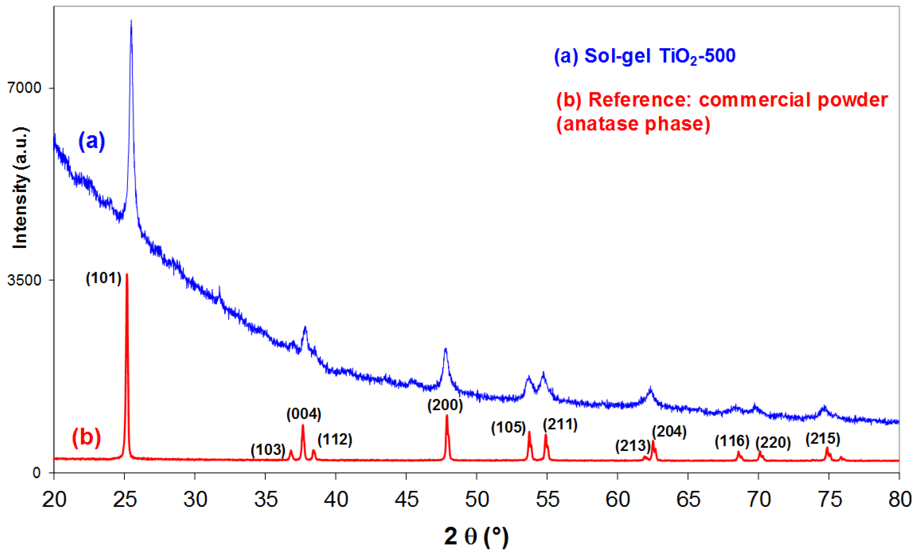
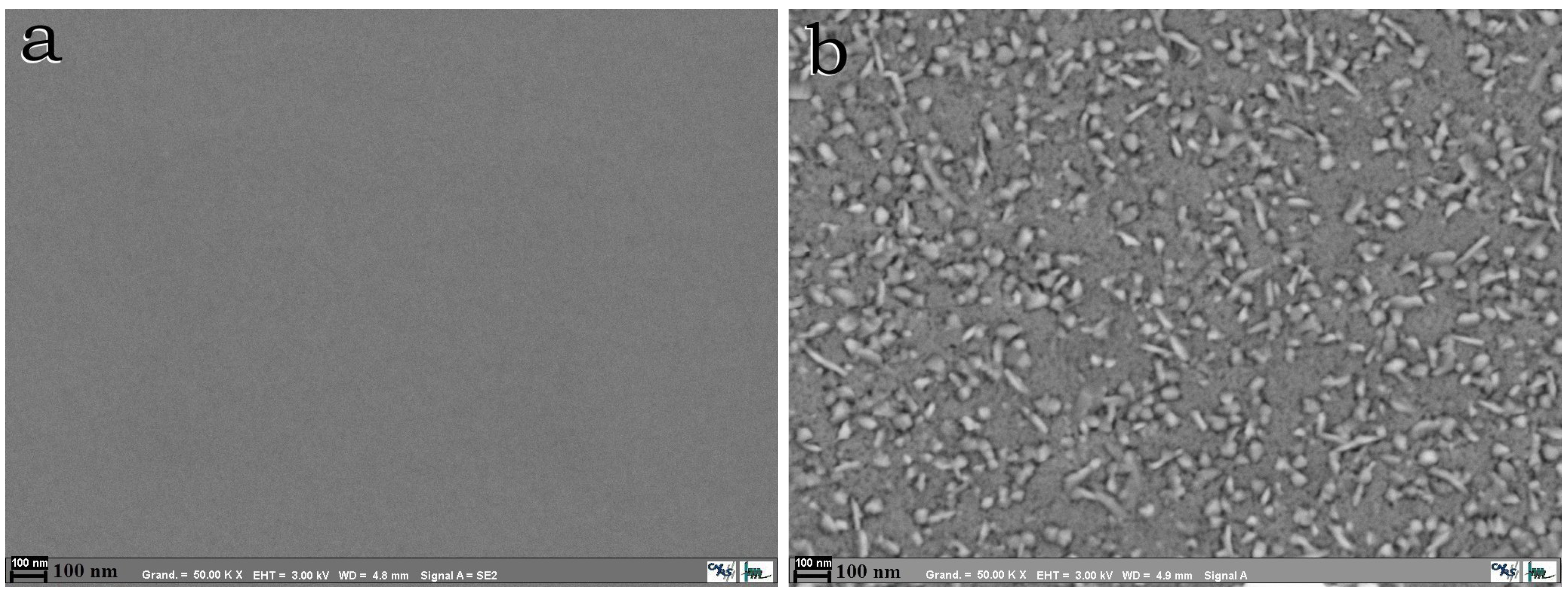
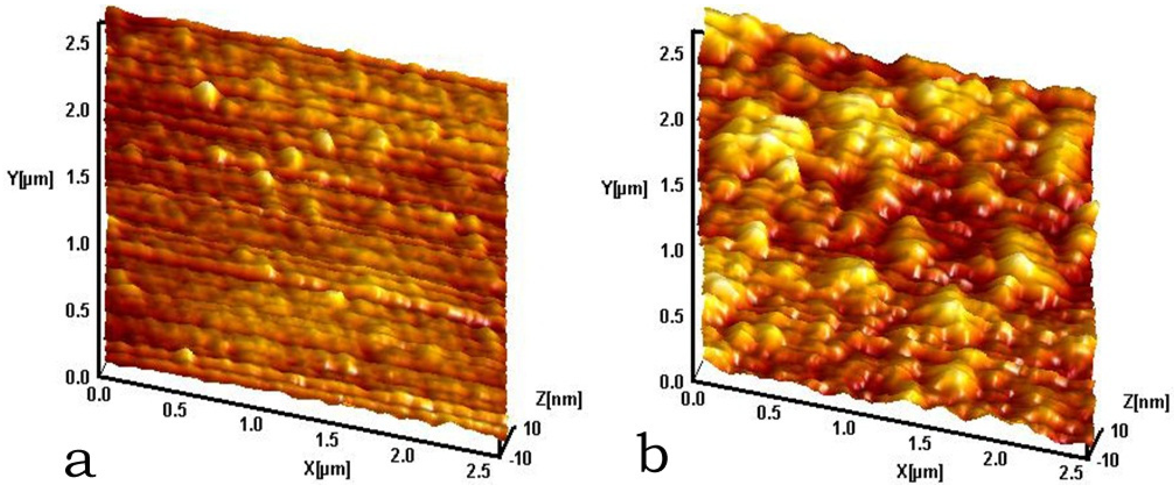
3.1. Morphological Characterizations


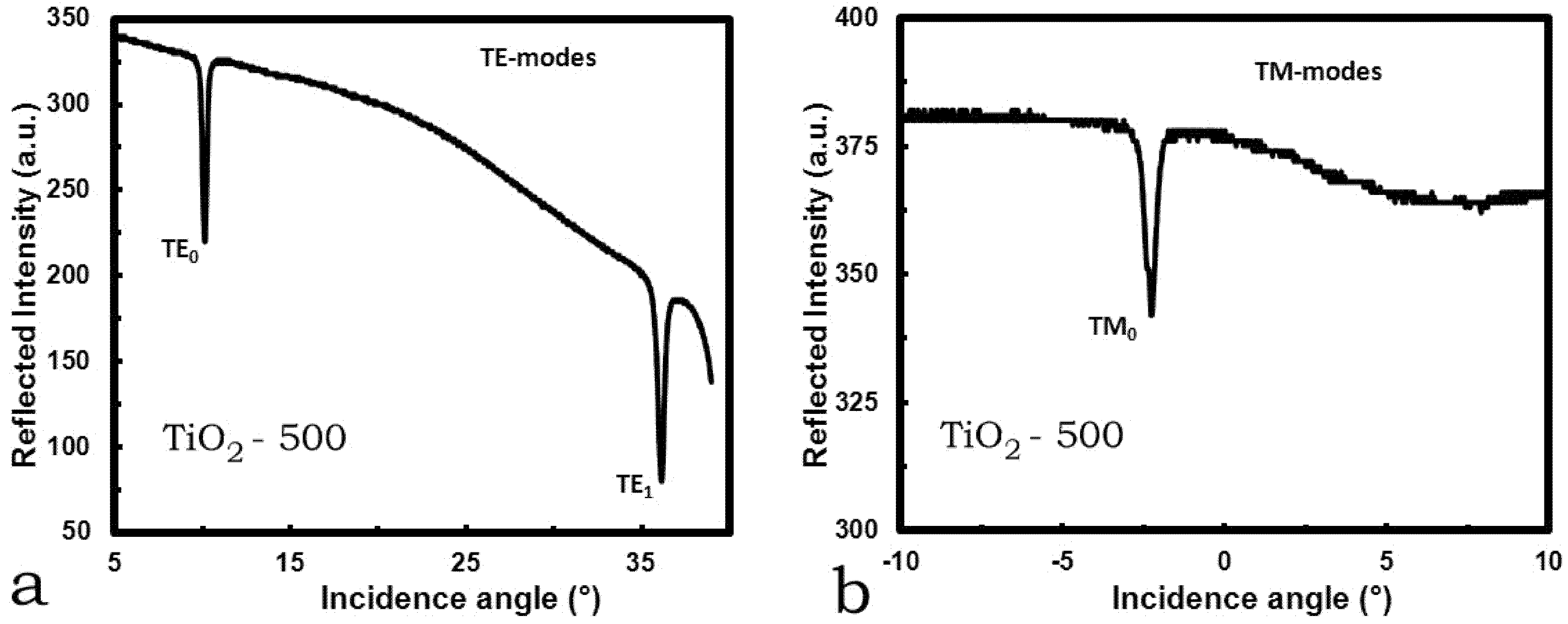
3.2. Optical Characterizations


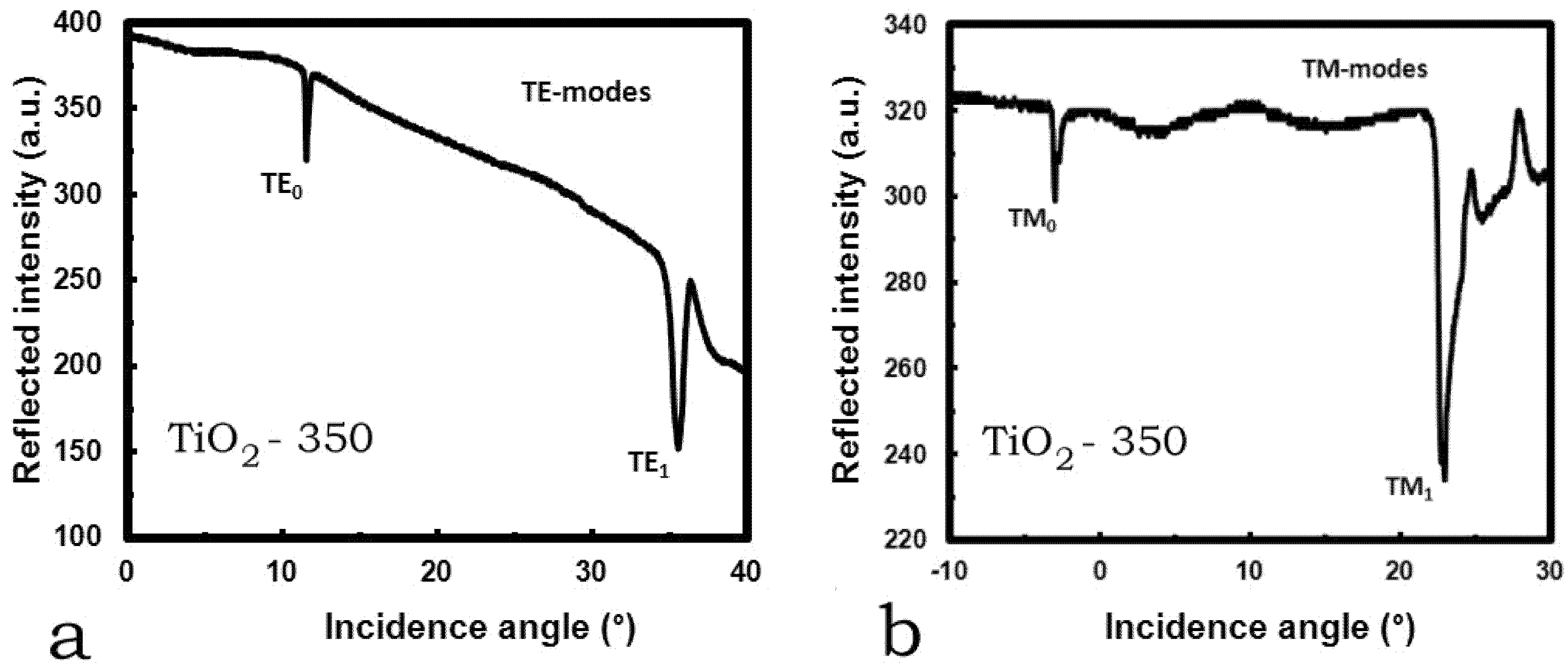
| Sample | Polarization | m | Nm exp. | Nm th. | ΔNm | n | d (nm) |
|---|---|---|---|---|---|---|---|
| TiO2-350 | TE | 0 | 1.8687 | 1.8685 | 2 × 10⁻⁴ | 1.9720 | 358 |
| TE | 1 | 1.5664 | 1.5659 | 5 × 10⁻⁴ | |||
| TM | 0 | 1.8444 | 1.8442 | 2 × 10⁻⁴ | 1.9895 | ||
| TM | 1 | 1.5135 | 1.5134 | 1 × 10⁻⁴ | |||
| TiO2-500 | TE | 0 | 1.8816 | 1.8814 | 2 × 10⁻⁴ | 1.9949 | 336 |
| TE | 1 | 1.5532 | 1.5527 | 5 × 10⁻⁴ | |||
| TM | 0 | 1.8479 | 1.8475 | 4 × 10⁻⁴ | 2.0092 |

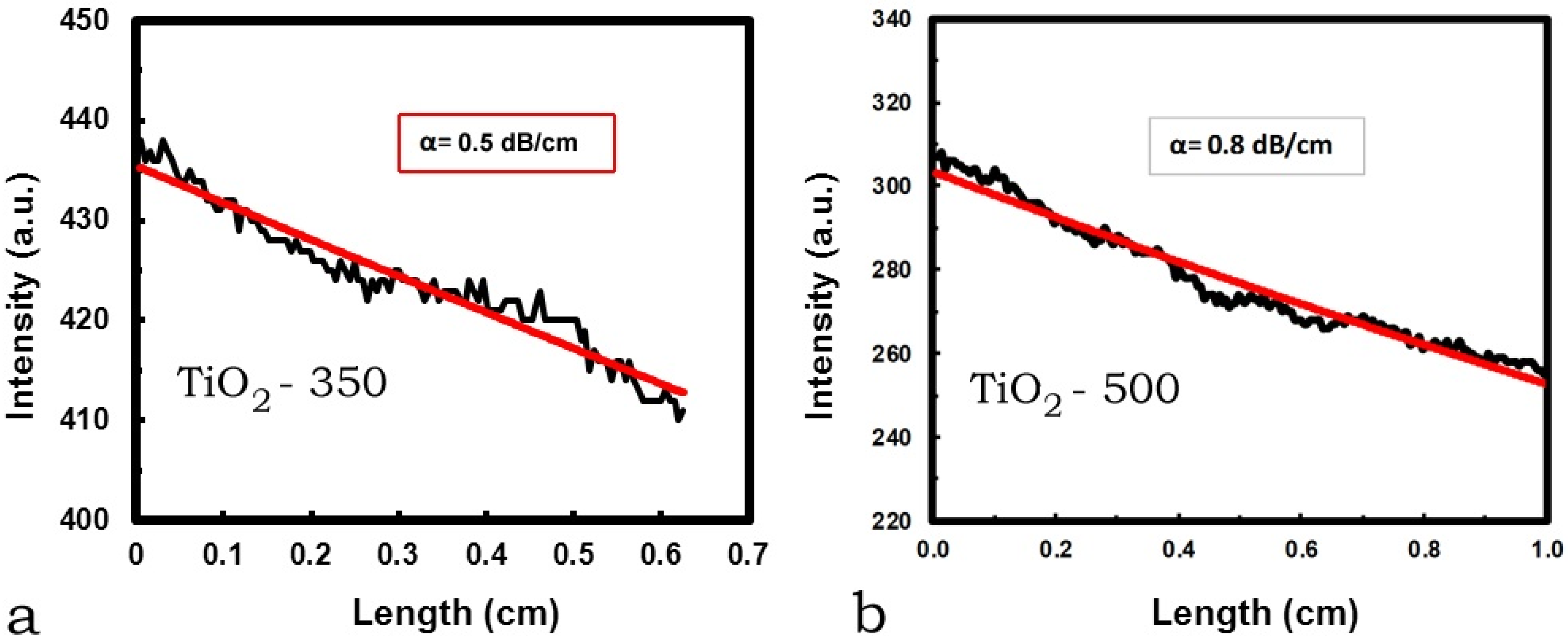
| Sample | H.T.T (°C) * | Structure [22] | Thickness: d (nm) | RMS (nm) | Refractive index: n | Attenuation: α (dB/cm) |
|---|---|---|---|---|---|---|
| TiO2-350 | 350 | Amorphous | 358 | 1.65 | 1.9720 | 0.5 |
| TiO2-500 | 500 | Crystallized | 336 | 3.26 | 1.9949 | 0.8 |
4. Conclusions
Acknowledgments
References
- Yamasaki, S.; Hata, N.; Yoshida, T.; Oheda, H.; Matsuda, A.; Okushi, H.; Tanaka, K. Annealing studies on low optical absorption of GD a-Si:H using photoacoustic spectroscopy. J. Phys. Colloq. 1981, 42, C4-297–C4-300. [Google Scholar]
- Brudnik, A.; Czternastek, H.; Zakrzewska, K.; Jachimowski, M. Plasma-emission-controlled d.c. magnetron sputtering of TiO2−x thin films. Thin Solid Films 1991, 199, 45–58. [Google Scholar]
- Garzella, C.; Comini, E.; Tempesti, E.; Frigeri, C.; Sberveglieri, G. TiO2 thin films by a novel sol-gel processing for gas sensor applications. Sens. Actuators B 2000, 68, 189–196. [Google Scholar] [CrossRef]
- San Vicente, G.; Morales, A.; Gutiérrez, M.T. Sol-gel TiO2 antireflective films for textured monocrystalline silicon solar cells. Thin Solid Films 2002, 403–404, 335–338. [Google Scholar]
- Wongcharee, K.; Brungs, M.; Chaplin, R.; Hong, Y.J.; Pillar, R. Sol-gel processing by aging and pore creator addition for porous silica antireflective coatings. J. Sol-Gel Sci. Technol. 2002, 25, 215–221. [Google Scholar]
- Yang, L.; Scott Saavedra, S.; Armstrong, N.R.; Hayes, J. Fabrication and characterization of low-loss, sol-gel planar waveguides. Anal. Chem. 1994, 66, 1254–1263. [Google Scholar] [CrossRef]
- Znaidi, L.; Seraphimova, R.; Bocquet, J.F.; Colbeau-Justin, C.; Pommier, C. A semi-continuous process for the synthesis of nanosize TiO2 powders and their use as photocatalysts. Mat. Res. Bull. 2001, 36, 811–825. [Google Scholar] [CrossRef]
- Montagna, M.; Moser, E.; Visintainer, F.; Ferrari, M.; Zampedri, L.; Martucci, A.; Guglielmi, M.; Ivanda, M. Nucleation of titania nanocrystals in silica titania waveguides. J. Sol-Gel Sci. Technol. 2003, 26, 241–244. [Google Scholar]
- Bernard, C.; Chaussedent, S.; Monteil, A.; Ferrari, M. Molecular dynamics simulation of an Er-activated silica-titania glass: Composition influence on the structural properties. Philos. Mag. B 2002, 82, 681–693. [Google Scholar]
- Yanagida, S.; Senadeera, G.K.R.; Nakamura, K.; Kitamura, T.; Wada, Y. Polythiophene-sensitized TiO2 solar cells. J. Photochem. Photobiol. A 2004, 166, 75–80. [Google Scholar] [CrossRef]
- Shen, J.; Yang, T.; Zhang, Q.; Wang, J. Nanoporous TiO2 coatings for infrared detectors. J. Sol-Gel Sci. Technol. 2003, 26, 1029–1032. [Google Scholar]
- Wang, Z.; Helmersson, U.; Käll, P.O. Optical properties of anatase TiO2 thin films prepared by aqueous sol-gel process at low temperature. Thin Solid Films 2002, 405, 50–54. [Google Scholar] [CrossRef]
- Pandiyan, R.; Micheli, V.; Ristic, D.; Bartali, R.; Pepponi, G.; Barozzi, M.; Gottardi, G.; Ferrari, M.; Laidani, N. Structural and near-infra red luminescence properties of Nd-doped TiO2 films deposited by RF sputtering. J. Mater. Chem. 2012, 22, 22424–22432. [Google Scholar] [CrossRef]
- Conde-Gallardo, A.; García-Rocha, M.; Palomino-Merino, R.; Velásquez-Quesada, M.P.; Hernández-Calderón, I. Photoluminescence properties of Tb3+ and Eu3+ ions hosted in TiO2 matrix. Appl. Surf. Sci. 2003, 212–213, 583–588. [Google Scholar]
- Wang, X.; Fujimaki, M.; Awazu, K. Photonic crystal structures in titanium dioxide (TiO2) and their optimal design. Opt. Express 2005, 13, 1486–1497. [Google Scholar] [CrossRef]
- Uhlmann, D.R.; Teowee, G. Sol-gel science and technology: Current state and future prospects. J. Sol-Gel Sci. Technol. 1998, 13, 153–162. [Google Scholar]
- Hench, L.L.; West, J.K. The sol-gel process. Chem. Rev. 1990, 90, 33–72. [Google Scholar] [CrossRef]
- Znaidi, L. Sol-gel-deposited ZnO thin films: A review. Mater. Sci. Eng. B 2010, 174, 18–30. [Google Scholar] [CrossRef]
- Nishide, T.; Sato, M.; Hara, H. Crystal structure and optical property of TiO2 gels and films prepared from Ti-edta complexes as titania precursors. J. Mater. Sci. 2000, 35, 465–469. [Google Scholar] [CrossRef]
- Oh, S.H.; Kim, D.J.; Hahn, S.H.; Kim, E.J. Comparison of optical and photocatalytic properties of TiO2 thin films prepared by electron-beam evaporation and sol-gel dip-coating. Mater. Lett. 2003, 57, 4151–4155. [Google Scholar] [CrossRef]
- Znaidi, L.; Bocquet, J.F.; Pommier, C. Elaboration of TiO2 nanometric powders and thin films aerogels. AIDIC conf. Ser. 2000, 4, 109–114. [Google Scholar]
- Znaidi, L.; Touam, T.; Vrel, D.; Kuznetsova, I.N.; Fischer, A.; Boudrioua, A. Waveguiding properties of nanostructured TiO2 thin films synthesized by sol-gel process. AIP Conf. Proc. 2011, 1400, 268–273. [Google Scholar]
- Ulrich, R. Theory of the prism-film coupler by plane-wave analysis. J. Opt. Soc. Am. 1970, 60, 1337–1350. [Google Scholar] [CrossRef]
- Mechiakh, R.; Ben Sedrine, N.; Ben Naceur, J.; Chtourou, R. Elaboration and characterization of nanocrystalline TiO2 thin films prepared by sol-gel dip-coating. Surf. Coat. Technol. 2011, 206, 243–249. [Google Scholar] [CrossRef]
- Urlacher, C.; Dumas, J.; Serughetti, J.; Mugnier, J.; Munoz, M. Planar ZrO2 waveguides prepared by the sol-gel process: Structural and optical properties. J. Sol-Gel Sci. Technol. 1997, 8, 999–1005. [Google Scholar]
- Tien, P.K.; Ulrich, R. Theory of prism-film coupler and thin-film light guides. J. Opt. Soc. Am. 1970, 60, 1325–1337. [Google Scholar] [CrossRef]
- Kersten, R.Th. Numerical solution of the mode-equation of planar dielectric waveguides to determine their refractive index and thickness by means of a prism-film coupler. Opt. Commun. 1973, 9, 427–431. [Google Scholar] [CrossRef]
- Wang, B.; Hu, L. Optical and surface properties of hybrid TiO2/ormosil planar waveguide prepared by the sol-gel process. Ceram. Int. 2006, 32, 7–12. [Google Scholar] [CrossRef]
- Strohkendl, F.P.; Fluck, D.; Günter, P.; Irmscher, R.; Buchal, Ch. Nonleaky optical waveguides in KNbO3 by ultralow dose MeV He ion implantation. Appl. Phys. Lett. 1991, 59, 3354–3356. [Google Scholar] [CrossRef]
- Weber, H.P.; Dunn, F.A.; Leibolt, W.N. Loss measurements in thin-film optical waveguides. Appl. Opt. 1973, 12, 755–757. [Google Scholar] [CrossRef]
- Boudrioua, A.; Loulergue, J.C. New approach for loss measurements in optical planar waveguides. Opt. Commun. 1997, 137, 37–40. [Google Scholar] [CrossRef]
- Ehrhart, G.; Capoen, B.; Robbe, O.; Boy, Ph.; Turrell, S.; Bouazaoui, M. Structural and optical properties of n-propoxide sol-gel derived ZrO2 thin films. Thin Solid Films 2006, 496, 227–233. [Google Scholar] [CrossRef]
- Bahtat, M.; Mugnier, J.; Lou, L.; Serughetti, J. Planar TiO2 waveguides by the sol-gel process: The relationship of structure to properties. SPIEProc. 1992, 1758, 173. [Google Scholar]
© 2013 by the authors; licensee MDPI, Basel, Switzerland. This article is an open access article distributed under the terms and conditions of the Creative Commons Attribution license (http://creativecommons.org/licenses/by/3.0/).
Share and Cite
Touam, T.; Znaidi, L.; Vrel, D.; Ninova-Kuznetsova, I.; Brinza, O.; Fischer, A.; Boudrioua, A. Low Loss Sol-Gel TiO2 Thin Films for Waveguiding Applications. Coatings 2013, 3, 49-58. https://doi.org/10.3390/coatings3010049
Touam T, Znaidi L, Vrel D, Ninova-Kuznetsova I, Brinza O, Fischer A, Boudrioua A. Low Loss Sol-Gel TiO2 Thin Films for Waveguiding Applications. Coatings. 2013; 3(1):49-58. https://doi.org/10.3390/coatings3010049
Chicago/Turabian StyleTouam, Tahar, Lamia Znaidi, Dominique Vrel, Iva Ninova-Kuznetsova, Ovidiu Brinza, Alexis Fischer, and Azzedine Boudrioua. 2013. "Low Loss Sol-Gel TiO2 Thin Films for Waveguiding Applications" Coatings 3, no. 1: 49-58. https://doi.org/10.3390/coatings3010049